Inrush Current Control of High Power Density DC–DC Converter


Abstract
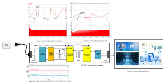
1. Introduction
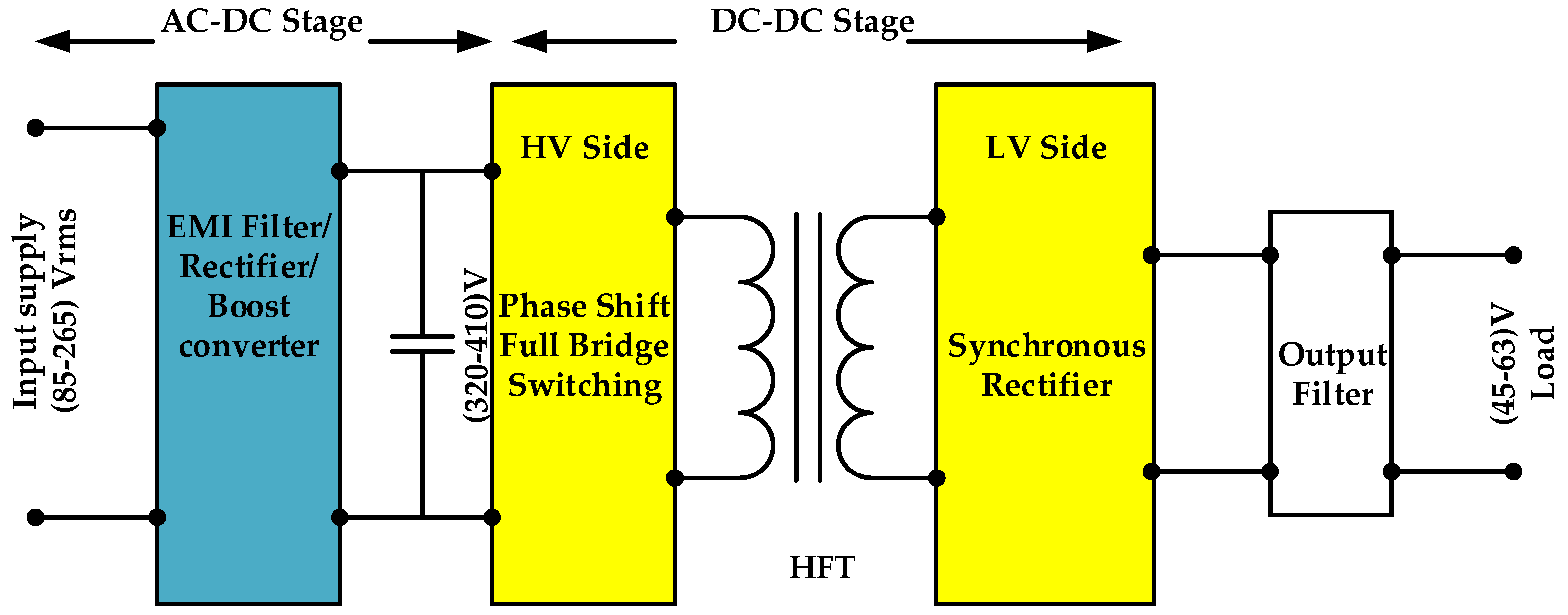
2. Design Procedure of the DC–DC Stage of the Telecom Power Supply
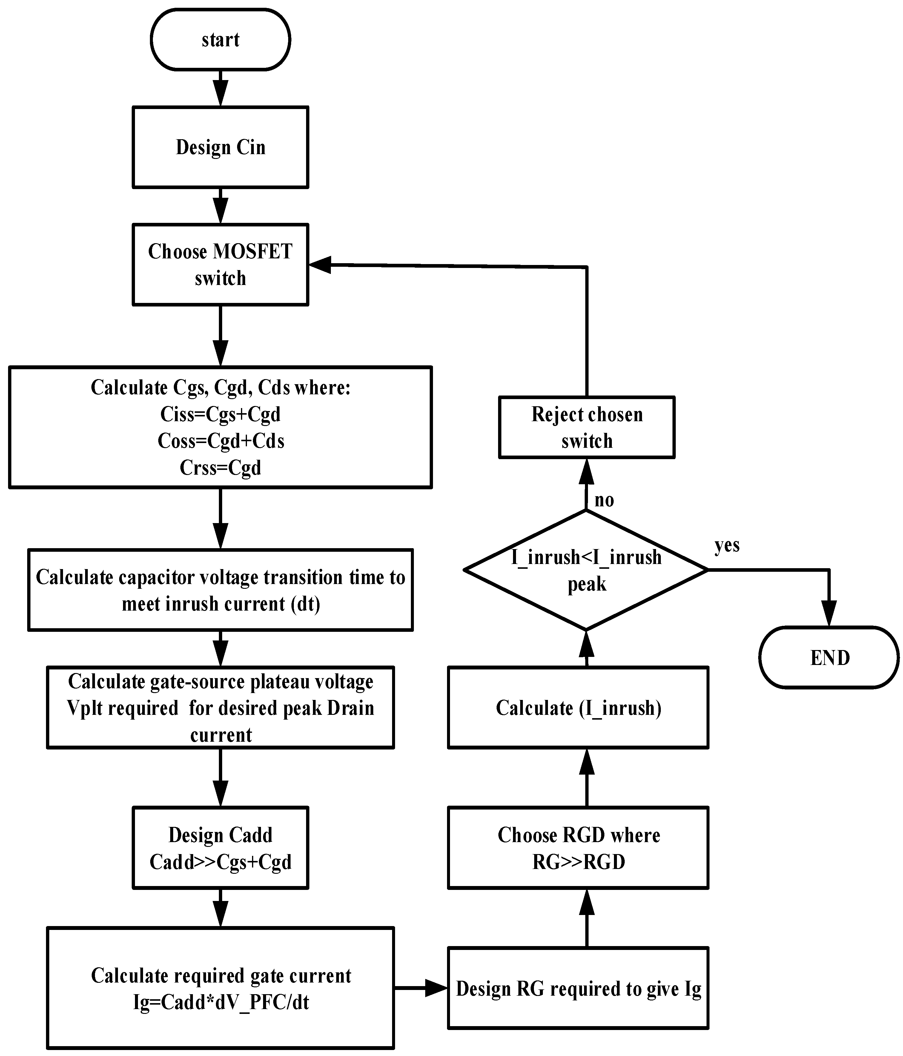
2.1. Input Capacitor Design
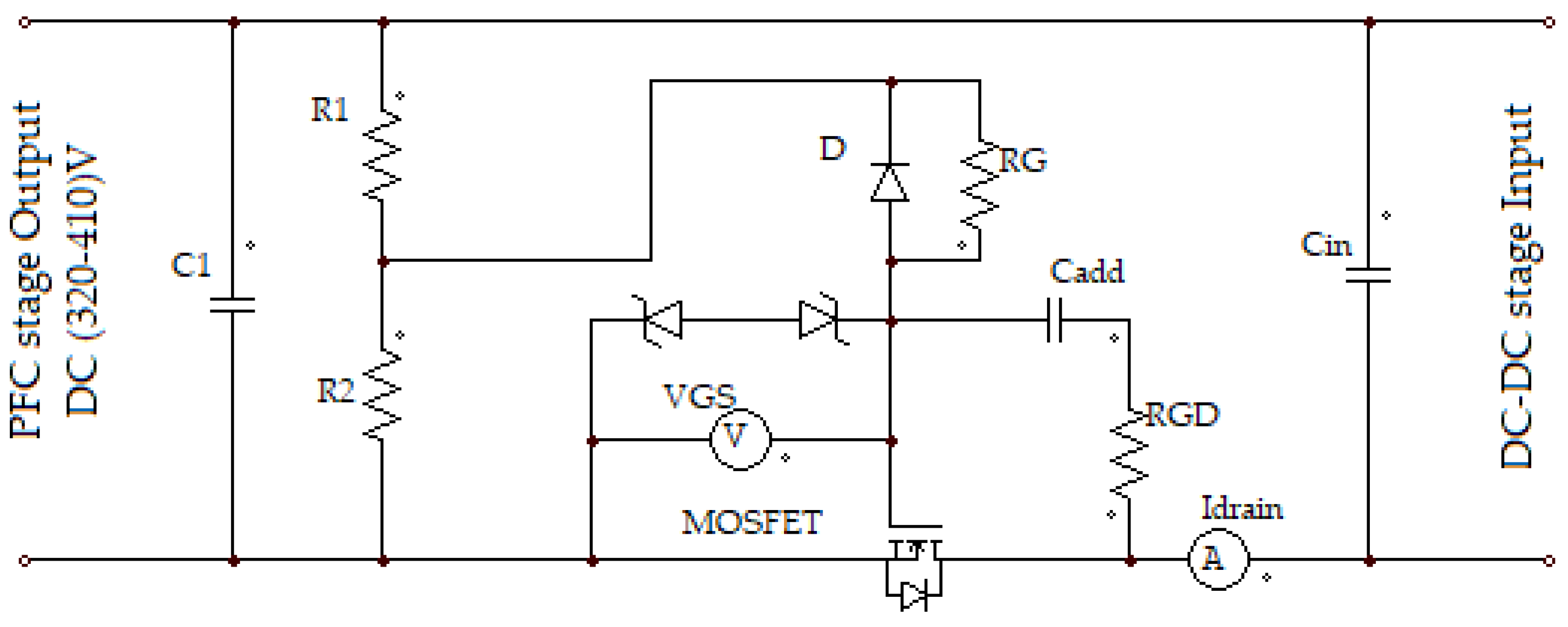
2.2. Proposed Inrush Current Control Circuit
2.3. Transformer (TR1) Turns Ratio (a) and Magentizing Reactance (Lm) Calculation
2.4. Resonant Inductor (Lr) Design
2.5. Output Inductance and Capacitance (Lload and Cload)
2.6. DC–DC Converter Controller Design and Implmentation
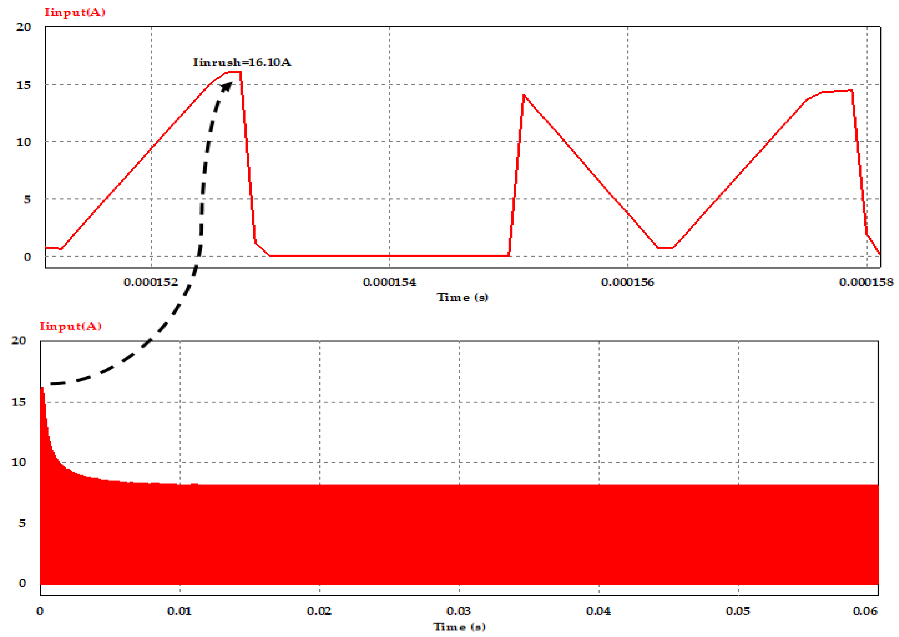
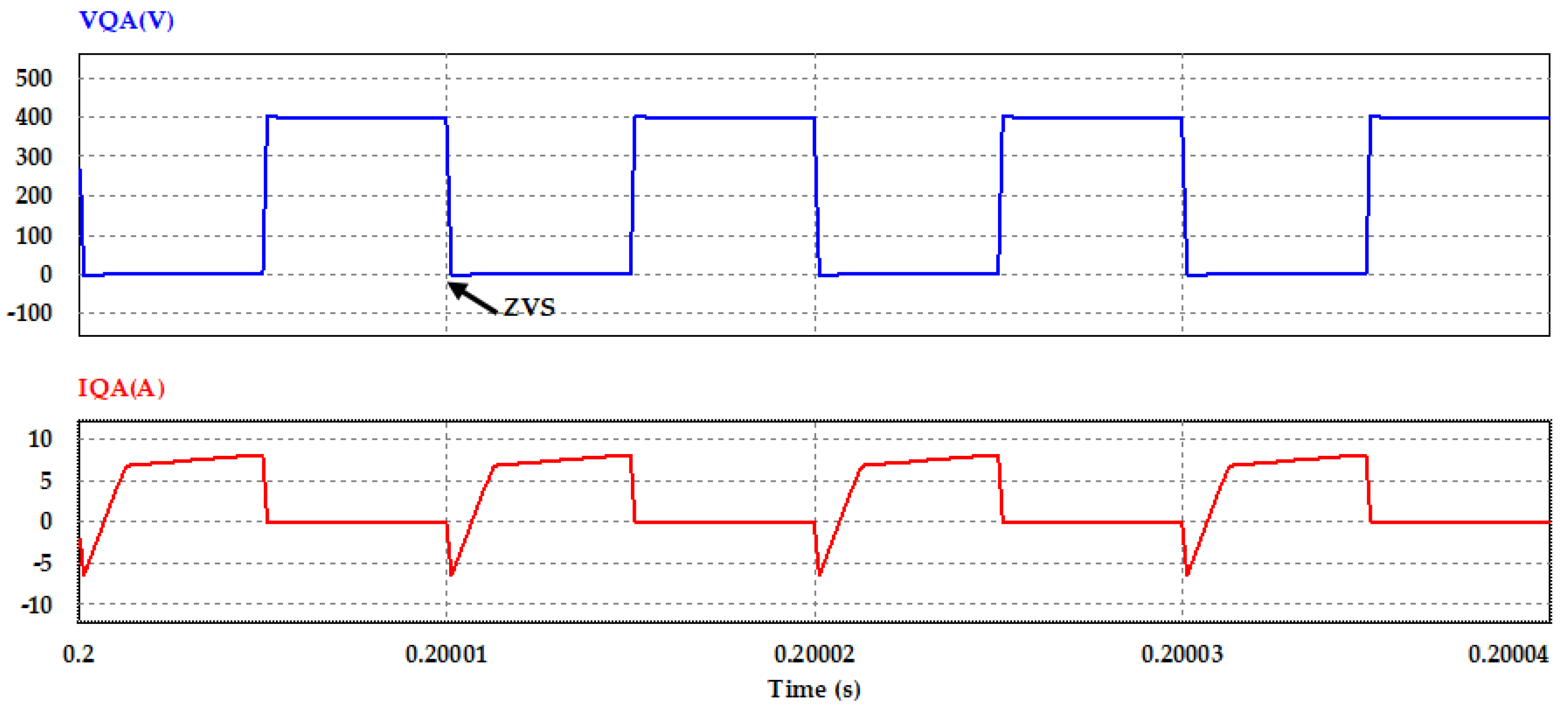
3. Simulation Results and Discussions
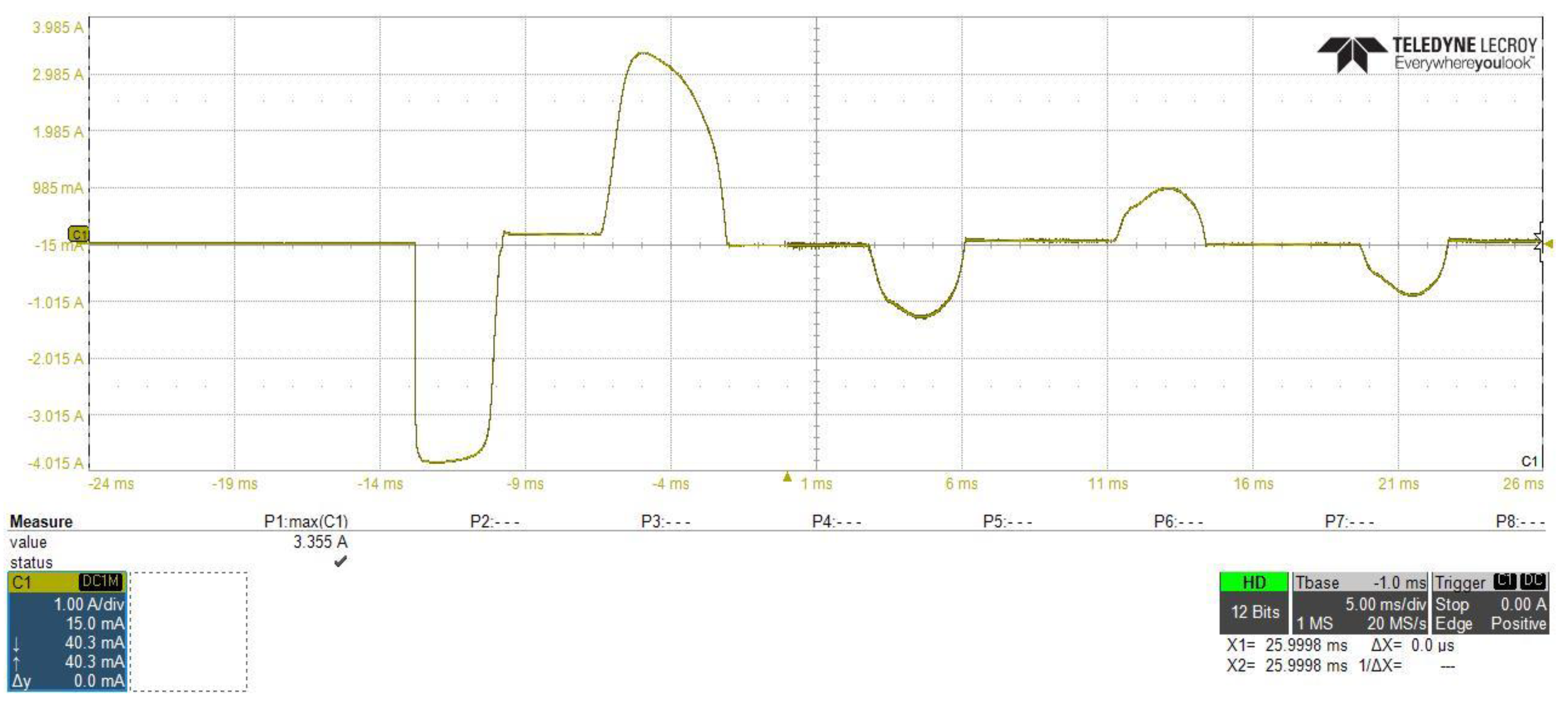
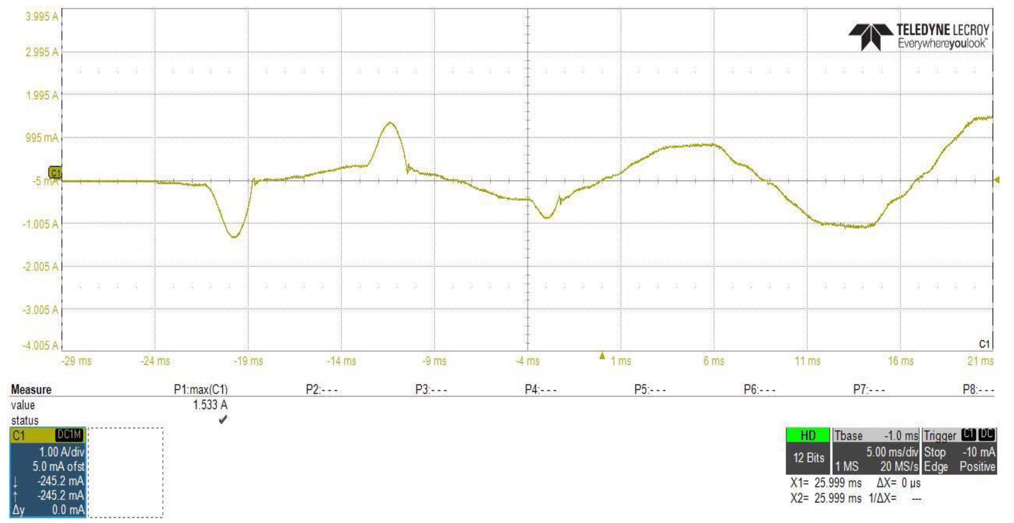
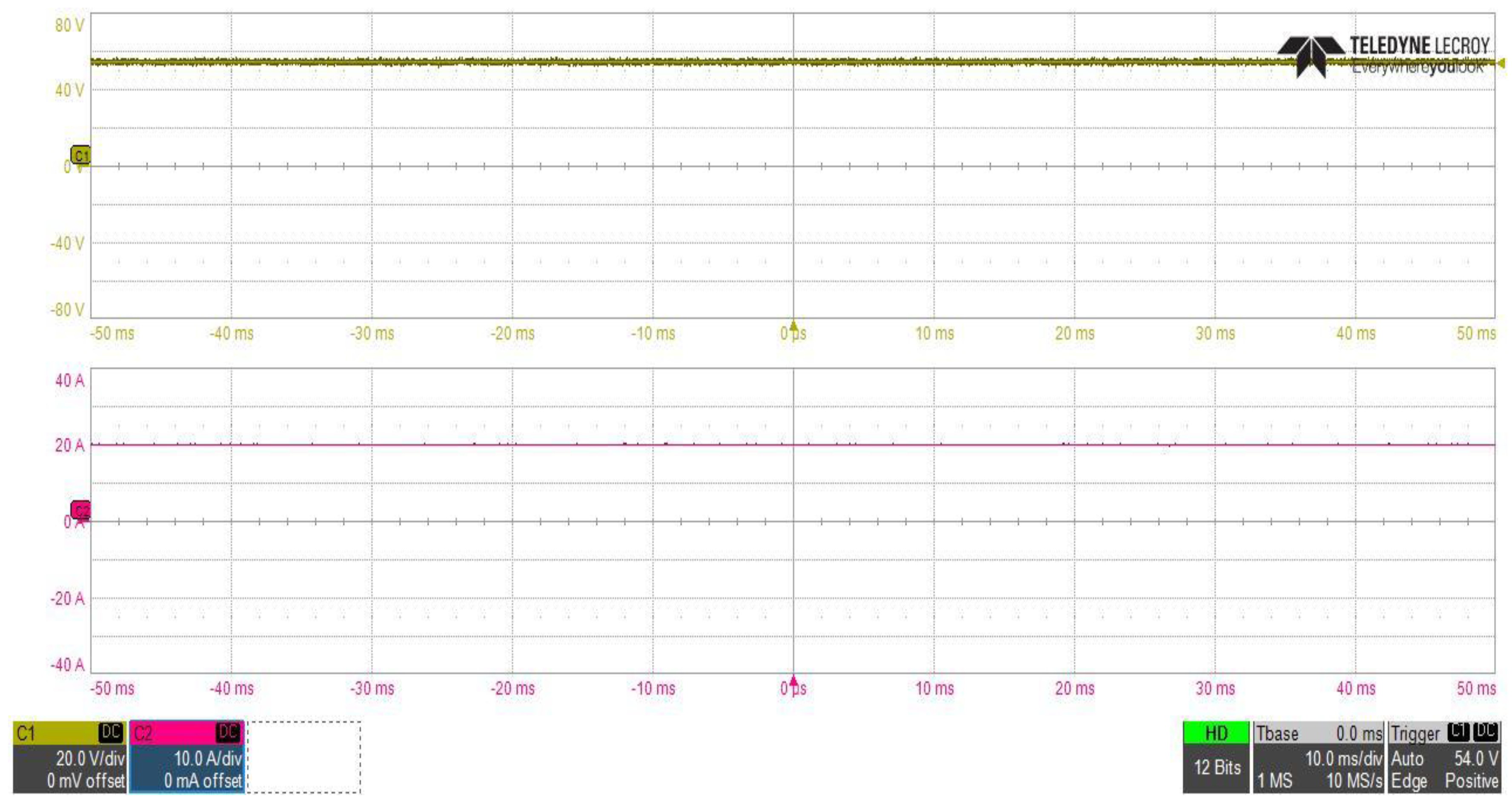
4. Experimental Setup
- Compact design and easy implementation with cheap passive elements and single MOSFET.
- Controllability and reliability of the circuit to limit the inrush current at the required value.
- Reduce the current stress on the input side of the two stages of power supply at initial power application.
- Improve the PFC stage performance by reducing the total reactive power consumption of the circuit.
- Easy to disconnect and reconnect again between two stages of a faulty case as compared with the IC soft starter (in case where the IC soft starter function is damaged).
- Ability to use with analog and digital control converter.
5. Conclusions
Author Contributions
Funding
Conflicts of Interest
References
- Garcia, O.; Cobos, J.A.; Prieto, R.; Alou, P.; Uceda, J. Single phase power factor correction: A survey. IEEE Trans. Power Electron. 2003, 18, 749–755. [Google Scholar] [CrossRef]
- Geddam, D.P.; Prakash, D.; Bapu, S.R.; Kumar, Y.R.; Rao, P.S.; Naidu, G.K.M.; Ramanarayanan, V. Design of 1.4 kw telecom rectifier delivering full power from 90Vac to 300Vac. In Proceedings of the IEEE INTELEC 07–29th International Telecommunications Energy Conference, Rome, Italy, 30 September–4 October 2007; pp. 670–676. [Google Scholar]
- Kasper, M.; Bortis, D.; Deboy, G.; Kolar, J.W. Design of a Highly Efficient (97.7%) and Very Compact (2.2 kW/dm3) Isolated AC–DC Telecom Power Supply Module Based on the Multicell ISOP Converter Approach. IEEE Trans. Power Electron. 2016, 32, 7750–7769. [Google Scholar] [CrossRef]
- Sekar, A.; Raghavan, D. Implementation of single phase soft switched PFC converter for plug-in-hybrid electric vehicles. Energies 2015, 8, 13096–13111. [Google Scholar] [CrossRef]
- Kim, Y.-S.; Sung, W.; Lee, B. Comparative performance analysis of high density and efficiency PFC topologies. IEEE Trans. Power Electron. 2003, 6, 2666–2679. [Google Scholar] [CrossRef]
- Biela, J.; Badstuebner, U.; Kolar, J.W. Impact of power density maximization on efficiency of DC–DC converter systems. IEEE Trans. Power Electron. 2009, 24, 288–300. [Google Scholar] [CrossRef]
- Yang, B.; Duarte, J.L.; Li, W.; Yin, K.; He, X.; Deng, Y. Phase-shifted full bridge converter featuring ZVS over the full load range. In Proceedings of the IECON 36th Annual Conference on IEEE Industrial Electronics Society, Glendale, AZ, USA, 7–10 November 2010; pp. 644–649. [Google Scholar]
- Lo, Y.-K.; Lin, C.-H.; Hsieh, M.-I.; Lin, C.-H. Phase-shifted full-bridge series-resonant DC–DC converters for wide load variations. IEEE Trans. Ind. Electron. 2010, 58, 2572–2575. [Google Scholar] [CrossRef]
- Schmidt, J.C.M.; Maragaño, J.C.; Sartori, H.C.; Pinheiro, J.R. Design methodology to achieve high-efficiency isolated ZVS DC/DC converters. In Proceedings of the 2017 IEEE 8th International Symposium on Power Electronics for Distributed Generation Systems (PEDG), Florianopolis, Brazil, 17–20 April 2017; pp. 1–8. [Google Scholar]
- Badstuebner, U.; Biela, J.; Kolar, W.J. Design of an 99%-efficient, 5kW, phase-shift PWM DC–DC converter for telecom applications. In Proceedings of the 2010 Twenty-Fifth Annual IEEE Applied Power Electronics Conference and Exposition (APEC), Palm Springs, CA, USA, 21–25 February 2010; pp. 773–780. [Google Scholar]
- Bai, H.; Nie, Z.; Mi, C.C. Experimental comparison of traditional phase-shift, dual-phase-shift, and model-based control of isolated bidirectional DC–DC converters. IEEE Trans. Power Electron. 2009, 25, 1444–1449. [Google Scholar] [CrossRef]
- Xiangli, K.; Li, S.; Smedley, K.M. Decoupled PWM plus phase-shift control for a dual-half-bridge bidirectional DC–DC converter. IEEE Trans. Power Electron. 2017, 33, 7203–7213. [Google Scholar] [CrossRef]
- Hurley, W.G.; Wölfle, W.H. Transformers and Inductors for Power Electronics. Theory, Design and Applications; Wiley: London, UK, 2013. [Google Scholar]
- Koo, G.B.; Moon, G.W.; Youn, M.J. New zero-voltage-switching phase-shift full-bridge converter with low conduction losses. IEEE Trans. Power Electron. 2005, 52, 228–235. [Google Scholar] [CrossRef]
- Kathiresan, R.; Das, P.; Reindl, T.; Panda, S.K. A novel ZVS DC–DC full-bridge converter with hold-up time operation. IEEE Trans. Ind. Electron. 2017, 64, 4491–4500. [Google Scholar] [CrossRef]
- Das, P.; Laan, B.; Mousavi, S.A.; Moschopoulos, G. A non-isolated bidirectional ZVS-PWM active clamped DC–DC converter. IEEE Trans. Power Electron. 2009, 24, 553–558. [Google Scholar] [CrossRef]
- Bojoi, R.; Fusillo, F.; Raciti, A.; Musumeci, S.; Scrimizzi, F.; Rizzo, S. Full-Bridge DC–DC Power Converter for Telecom applications with Advanced Trench Gate MOSFETs. In Proceedings of the 2018 IEEE International Telecommunications Energy Conference (INTELEC), Lingnotto Fiere, Italy, 7–11 October 2018; pp. 1–7. [Google Scholar]
- Zhao, Z.; Xu, Q.; Dai, Y.; Yin, H. Analysis, Design, and Implementation of Improved LLC Resonant Transformer for Efficiency Enhancement. Energies 2018, 11, 3288. [Google Scholar] [CrossRef]
- Tao, H.; Zhang, G.; Zheng, Z.; Du, C. Design of Digital Control System for DC/DC Converter of On-Board Charger. J. Adv. Transp. 2019, 2019, 2467307. [Google Scholar] [CrossRef]
- Cho, J.-H.; Seong, H.-Y.; Jung, S.-H.; Park, J.-Y.; Moon, G.-U.; Youn, M.-Y. Implementation of digitally controlled phase shift full bridge converter for server power supply. In Proceedings of the 2010 IEEE Energy Conversion Congress and Exposition, Atlanta, GA, USA, 12–16 September 2010; pp. 802–809. [Google Scholar]
- Lee, Y.J.; Bak, Y.; Lee, K.Y. Control Method for Phase-Shift Full-Bridge Center-Tapped Converters Using a Hybrid Fuzzy Sliding Mode Controller. Electronics 2019, 8, 705. [Google Scholar] [CrossRef]
- Cho, I.-H.; Cho, K.-M.; Kim, J.-W.; Moon, G.-W. A new phase-shifted full-bridge converter with maximum duty operation for server power system. IEEE Trans. Power Electron. 2011, 26, 3491–3500. [Google Scholar] [CrossRef]
- Moisseev, S.; Soshin, K.; Sato, S.; Gamage, L.; Nakaoka, M. Novel soft-commutation DC–DC power converter with high-frequency transformer secondary side phase-shifted PWM active rectifier. IEE Electr. Power Appl. 2004, 151, 260–267. [Google Scholar] [CrossRef]
- Kim, Y.-D.; Cho, K.-M.; Kim, D.-Y.; Moon, G.-W. Wide-range ZVS phase-shift full-bridge converter with reduced conduction loss caused by circulating current. IEEE Trans. Power Electron. 2012, 28, 3308–3316. [Google Scholar] [CrossRef]
- Inrush Current in DC–DC Converters. Application Notes, vpt Power. Available online: http://www.vptpower.com/wp-content (accessed on 14 November 2019).
- Martínez-Salamero, L.; García, G.; Orellana, M.; Lahore, C.; Estibals, B. Start-up control and voltage regulation in a boost converter under sliding-mode operation. IEEE Trans. Ind. Electron. 2012, 60, 4637–4649. [Google Scholar] [CrossRef]
- Aroudi, A.E.; Martínez-Treviño, B.A.; Vidal-Idiarte, E.; Martínez-Salamero, L. Analysis of Start-Up Response in a Digitally Controlled Boost Converter with Constant Power Load and Mitigation of Inrush Current Problems. IEEE Trans. Circuits Syst. I 2019, 67, 1276–1285. [Google Scholar] [CrossRef]
- Mitter, S. Active Inrush Current Limiting Using MOSFETs; Motorola Inc.: Phoenix, AZ, USA, 1995; Available online: http://application-notes.digchip.com/010/10-13155.pdf (accessed on 10 January 2020).
- Kalenteridis; Vasileios; Agorastou, Z.; Siskos, S. A soft start-up technique for inrush current limitation in DC–DC converters. In Proceedings of the 2019 IEEE Panhellenic Conference on Electronics & Telecommunications (PACET), Volos, Greece, 8–9 November 2019; pp. 1–4. [Google Scholar]
- Ma, F.-F.; Chen, W.-Z.; Wu, J.-C. A monolithic current-mode buck converter with advanced control and protection circuits. IEEE Trans. Power Electron. 2007, 22, 1836–1846. [Google Scholar] [CrossRef]
- Sathishkumar, P.; Krishna, T.N.V.; Khan, M.A.; Zeb, K.; Kim, H. Digital soft start implementation for minimizing start up transients in high power DAB-IBDC converter. Energies 2018, 11, 956. [Google Scholar] [CrossRef]
- Managing Inrush Current. Application Report, Texas Instruments. Available online: http://www.ti.com/lit/an/slva670a/slva670a.pdf?&ts=1589053420769 (accessed on 12 January 2020).
- Jiang, T.; Cairoli, P.; Rodrigues, R.; Du, Y. Inrush current limiting for solid state devices using NTC resistor. In Proceedings of the IEEE Southeast Conference, Charlotte, NC, USA, 30 March–2 April 2017; pp. 1–7. [Google Scholar]
- NTC Thermistors Ordering Code. RS Components. Available online: https://docs.rs-online.com/ee83/0900766b80e7f61b.pdf (accessed on 12 January 2020).
- Dias, V.A.; Pomilio, J.A.; Finco, S. A current limiting switch for applications in space power systems. In Proceedings of the 2017 IEEE Southern Power Electronics Conference (SPEC), Puerto Valas, Chile, 4–7 December 2017; pp. 1–6. [Google Scholar]
- Fuengwarodsakul, N.H. Battery management system with active inrush current control for Li-ion battery in light electric vehicles. Electr. Eng. 2016, 98, 17–27. [Google Scholar] [CrossRef]
- Marroqui, D.; Garrigos, A.; Blanes, J.M.; Gutierrez, R. Photovoltaic-Driven SiC MOSFET Circuit Breaker with Latching and Current Limiting Capability. Energies 2019, 12, 4585. [Google Scholar] [CrossRef]
- Lee, E.-J.; Ahn, J.-H.; Shin, S.-M.; Lee, B.-K. Comparative analysis of active inrush current limiter for high-voltage DC power supply system. In Proceedings of the 2012 IEEE Vehicle Power and Propulsion Conference, Seoul, Korea, 9–12 October 2012; pp. 1256–1260. [Google Scholar]
- Musumeci, S. Gate charge control of high-voltage Silicon-Carbide (SiC) MOSFET in power converter applications. In Proceedings of the 2015 International Conference on Clean Electrical Power (ICCEP), Taormina, Italy, 16–18 June 2015; pp. 709–715. [Google Scholar]
- Manolarou, M.; Kostakis, G.; Manias, S.N. Inrush current limiting technique for low-voltage synchronous DC/DC converters. IEE Electr. Power Appl. 2005, 152, 1179–1183. [Google Scholar] [CrossRef]
- Manousaka, E. DC–DC Buck Converter with Inrush Current Limiter. Master’s Thesis, Faculty of Applied Sciences, Delft University of Technology, Delft, Wales, October 2013. [Google Scholar]
- UCC28950 600-W, Phase-Shifted, Full-Bridge Application Report. Texas Instruments. Available online: http://www.ti.com/lit/slua560 (accessed on 8 March 2020).
- N-CHANNEL 500 V –0.105Ω –31A TO-247 Zener-Protected MOSFET. Available online: https://www.st.com/resource/en/datasheet/cd00045267.pdf (accessed on 5 April 2020).
- “Power Electronics Handbook” Book; Available online: http://site.iugaza.edu.ps/malramlawi/files/RASHID_Power_Electronics_Handbook.pdf (accessed on 25 February 2020).
- Phase-Shifted Full-Bridge, Zero-Voltage Transition Design Considerations. Application Report. Available online: https://www.ti.com/lit/pdf/slua107 (accessed on 8 March 2020).
- Instruments Texas. Modeling, Analysis and Compensation of the Current-Mode Converter; Notes, Application; Texas Instruments Inc.: Dallas, TX, USA, 1999. [Google Scholar]
- 2.5kW PFC Evaluation Board with CCM PFC Controller ICE3PCS01G. Design Report, Infineon Company. Available online: https://www.infineon.com/cms/en/product/evaluation-boards/eval_2k5w_ccm_4p_v3/ (accessed on 15 April 2020).
- IEC/EN61000 Standards for Power Supplies. SL Power Application Note. Available online: https://slpower.com/App-slpower/images/whitepapers/AN-G007_EN61000.pdf (accessed on 12 August 2020).


| Parameter | Value | Unit |
|---|---|---|
| Input capacitance (Cin) | 350 | uF |
| Chosen MOSFET | STW20NK50Z | - |
| Cadd | 0.1 | uF |
| RG | 30 | kΩ |
| RGD | 500 | Ω |
| R1 | 715 | kΩ |
| R2 | 84.5 | kΩ |
| Allowable Inrush peak | 9 | A |
| Plat voltage (Vplt) | 4.35 | V |
| Gate current (Ig) | 3.430 | mA |
| Parameter | Value | Unit |
|---|---|---|
| Input voltage | 400 (320–410) | V |
| Output voltage | 54 (45–63) | V |
| Output voltage transient (Vtran) | 1 | Vpp |
| Rated power | 2 | kW |
| Switching frequency | 100 | kHz |
| Designed efficiency | 95% | - |
| Input voltage hold up time (thold) | 4 | ms |
| Input capacitor (Cin) | 350 | uF |
| Transformer turns ratio | 20/4/4 | Np/Ns/Nt |
| Transformer reactance (Lmag) | 2.8 | mH |
| Primary switches | IPW60R070CFD7 | - |
| Secondary switches | IPP110N20N3 | - |
| Output capacitor (Cload) | 2750 | uF |
| Output Inductor (Lload) | 22 | uH |
| Resonant inductor (Lr) | 30 | uH |
© 2020 by the authors. Licensee MDPI, Basel, Switzerland. This article is an open access article distributed under the terms and conditions of the Creative Commons Attribution (CC BY) license (http://creativecommons.org/licenses/by/4.0/).
Share and Cite
Okilly, A.H.; Kim, N.; Baek, J. Inrush Current Control of High Power Density DC–DC Converter. Energies 2020, 13, 4301. https://doi.org/10.3390/en13174301
Okilly AH, Kim N, Baek J. Inrush Current Control of High Power Density DC–DC Converter. Energies. 2020; 13(17):4301. https://doi.org/10.3390/en13174301
Chicago/Turabian StyleOkilly, Ahmed H., Namhun Kim, and Jeihoon Baek. 2020. "Inrush Current Control of High Power Density DC–DC Converter" Energies 13, no. 17: 4301. https://doi.org/10.3390/en13174301
APA StyleOkilly, A. H., Kim, N., & Baek, J. (2020). Inrush Current Control of High Power Density DC–DC Converter. Energies, 13(17), 4301. https://doi.org/10.3390/en13174301