Methods of Modulation for Current-Source Single-Phase Isolated Matrix Converter in a Grid-Connected Battery Application


Abstract
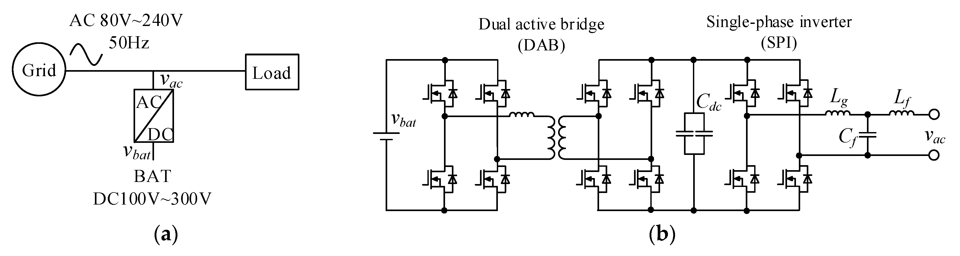
:1. Introduction
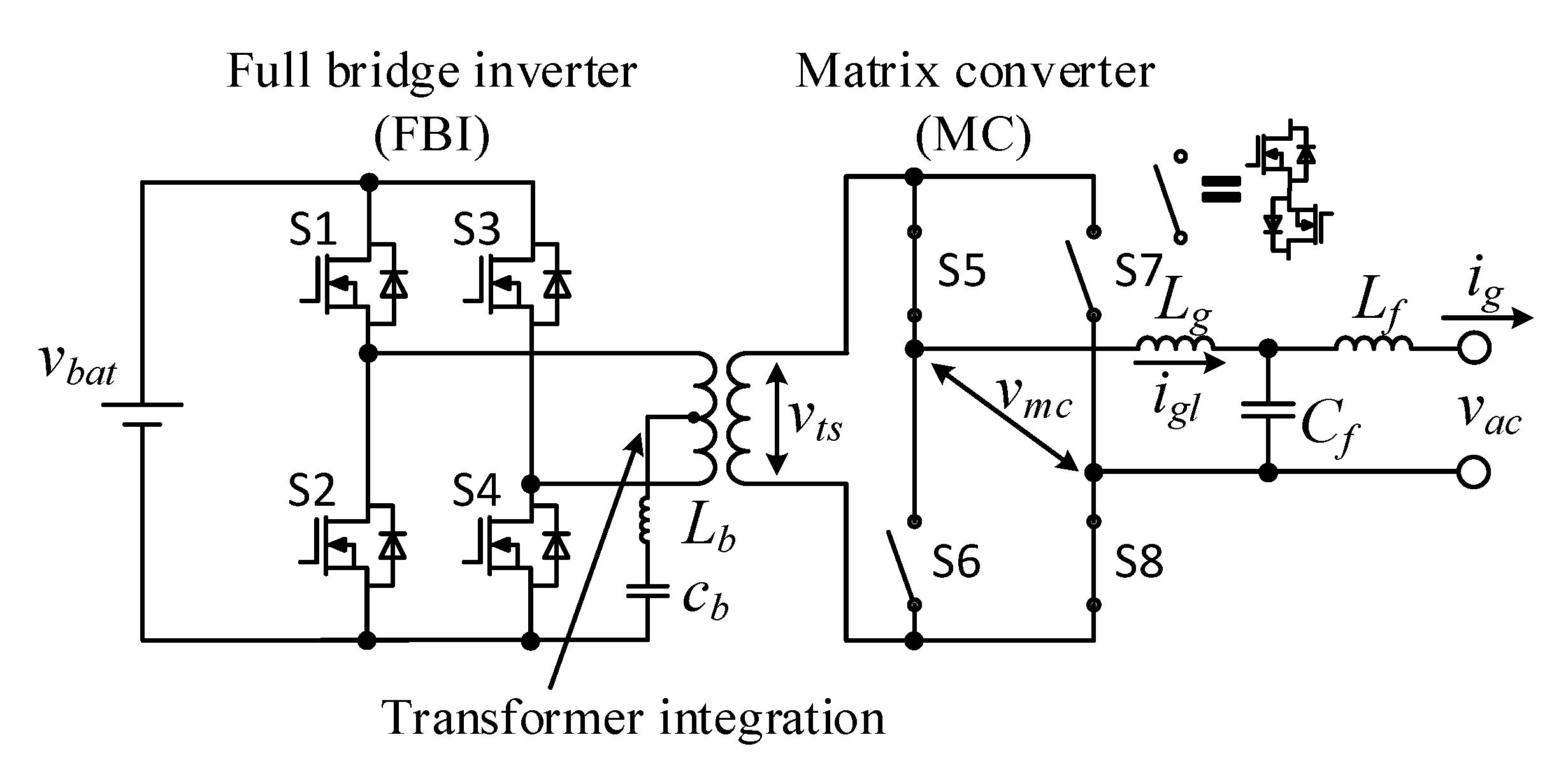
2. Control Scheme
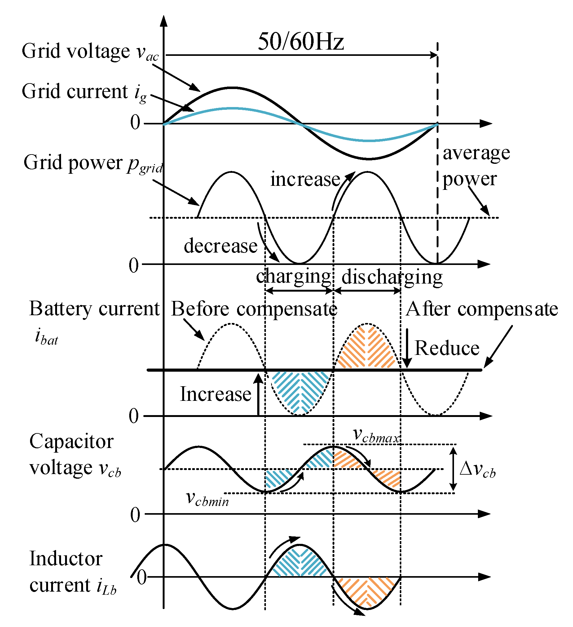
2.1. System Control
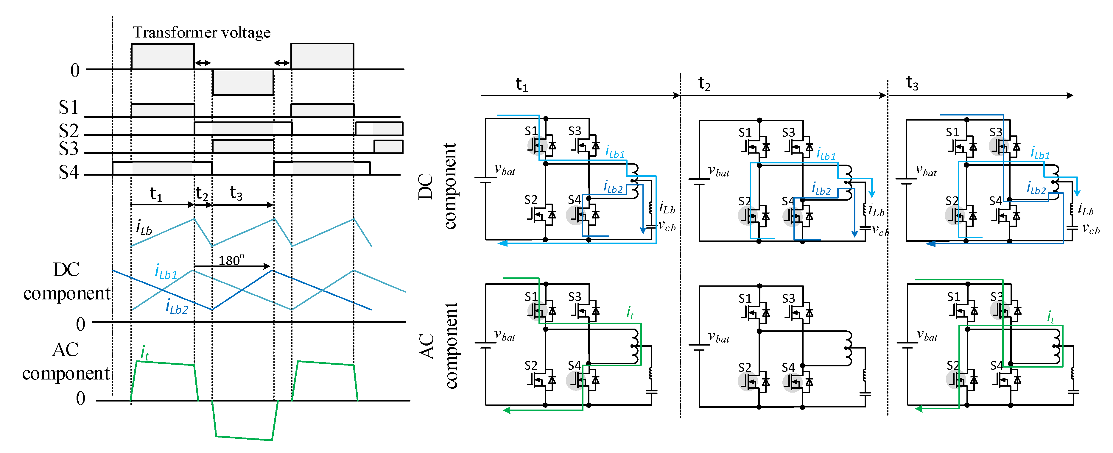
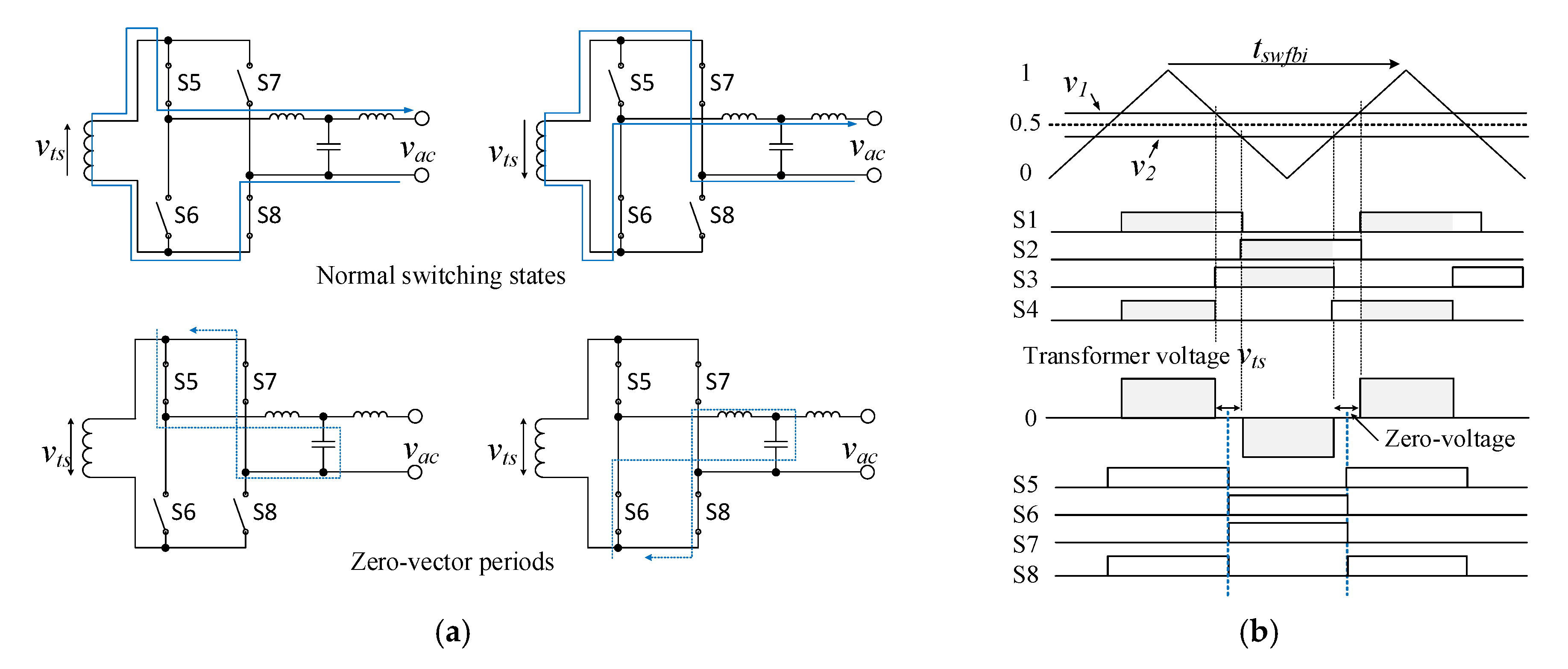
2.2. Switching Behaviors in FBI
2.3. Modulation in MC
3. Methods of Modulation
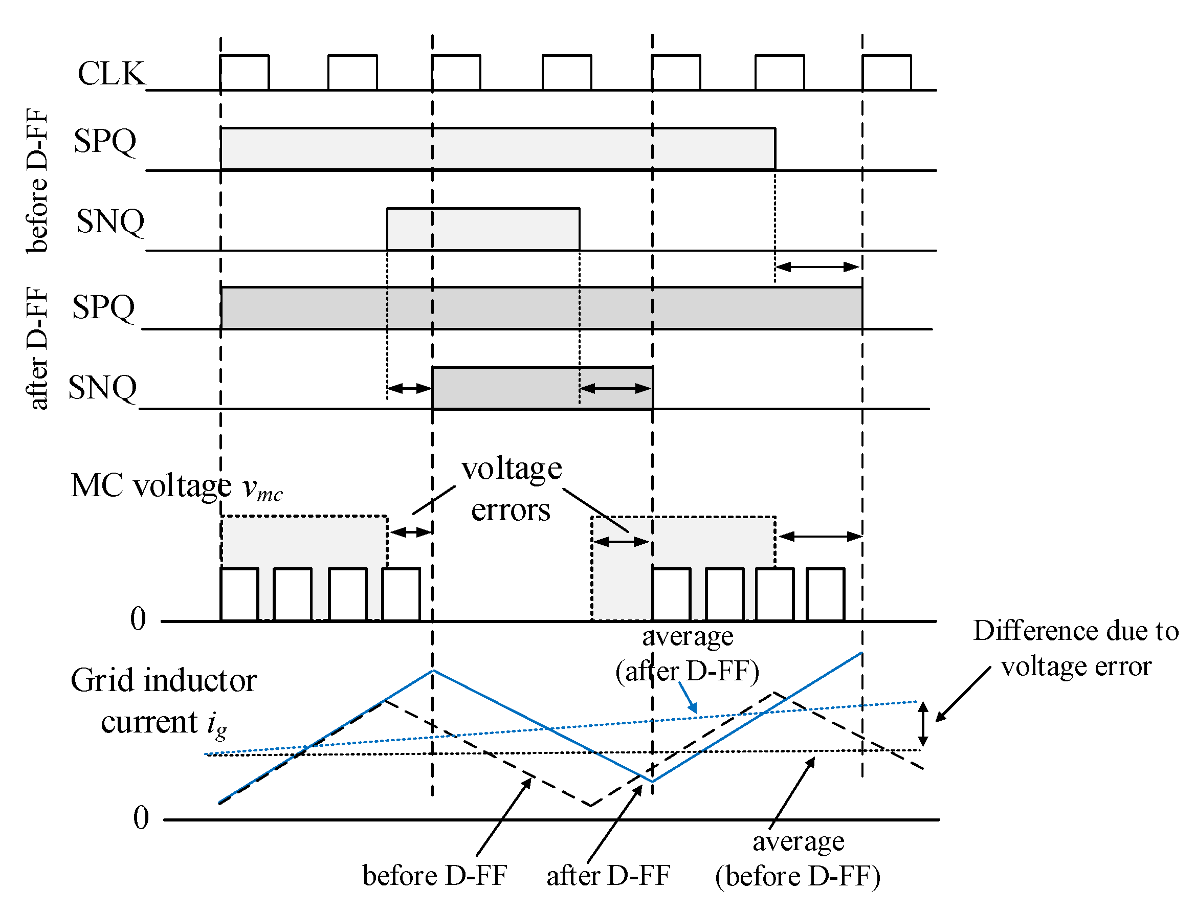
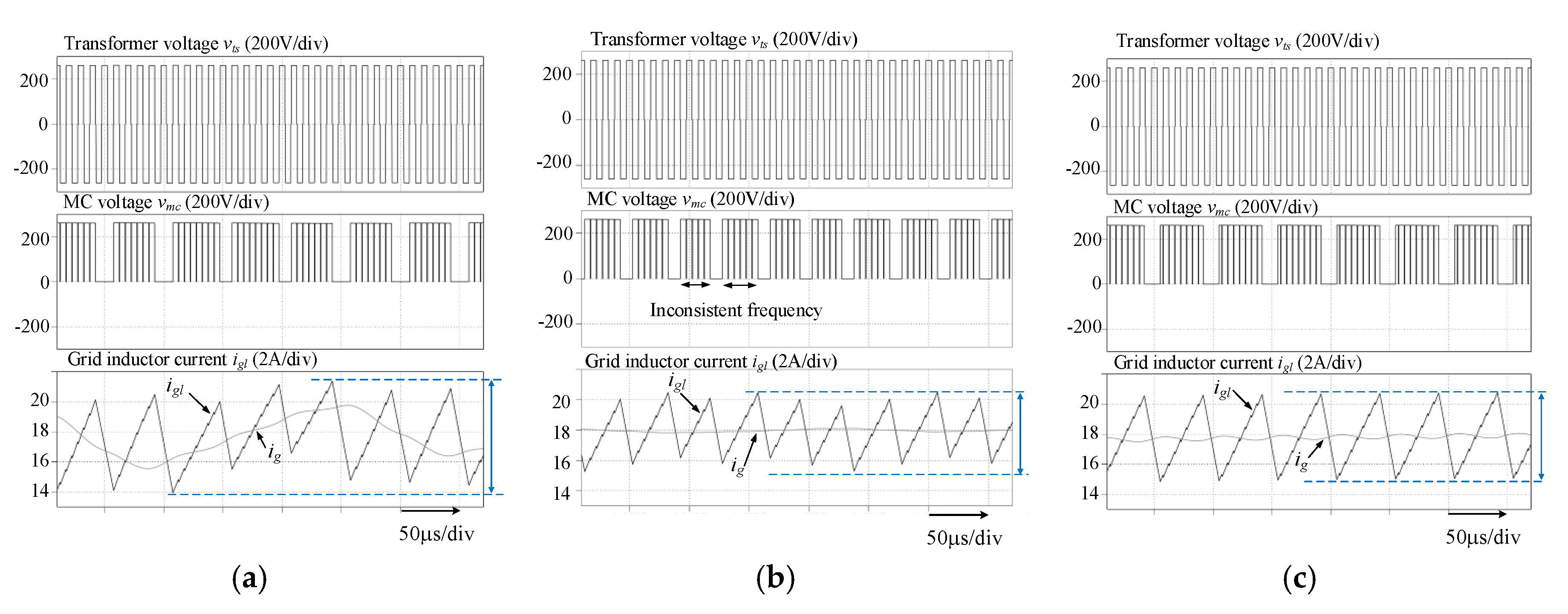
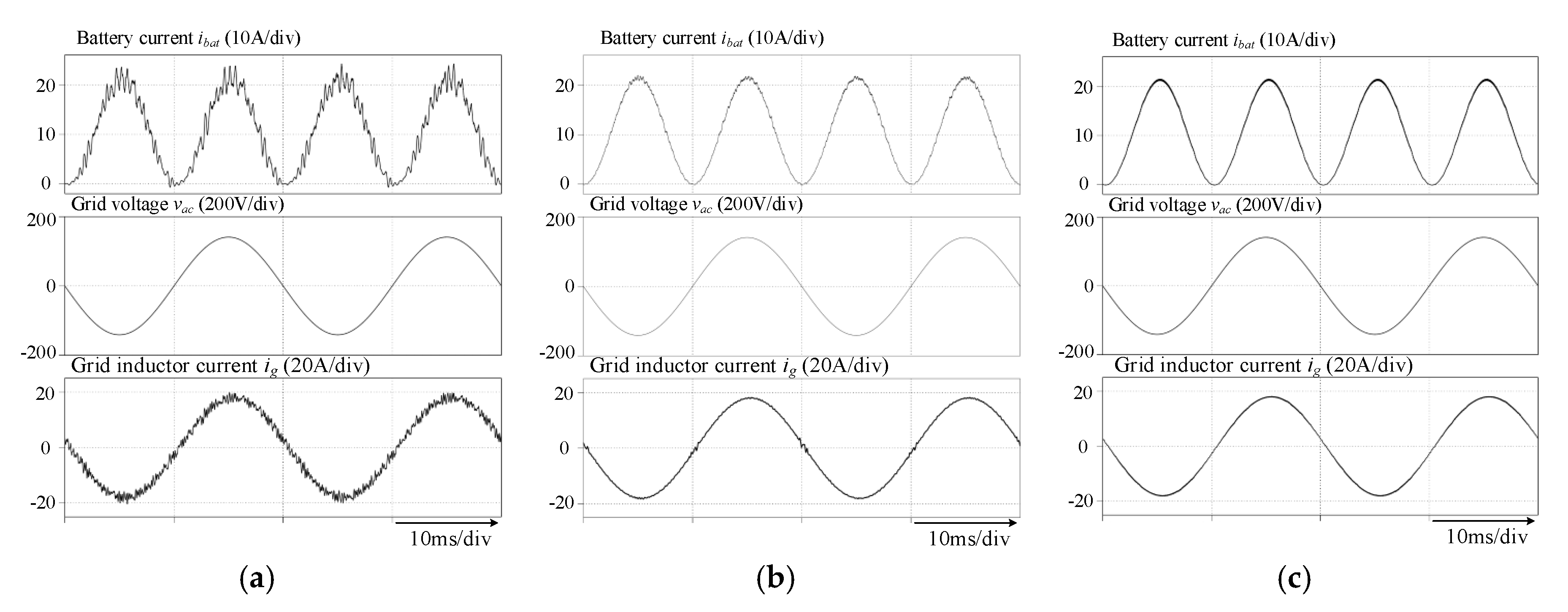
3.1. Carrier Comparison with D-FF (D-FlipFlop)
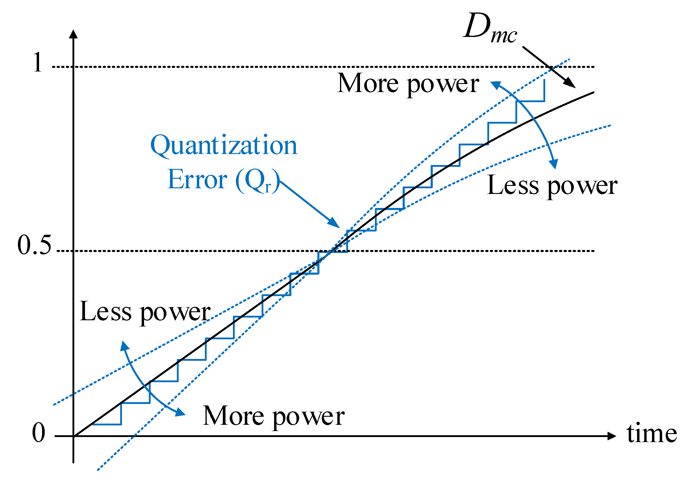
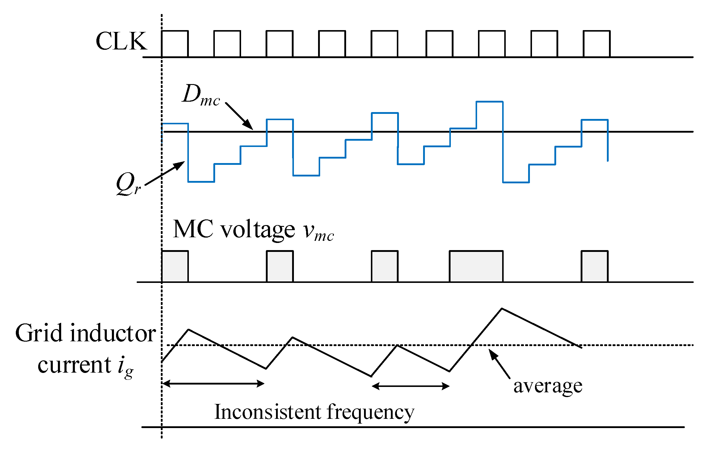
3.2. Delta-Sigma Conversion with Pulse Density Modulation (PDM)
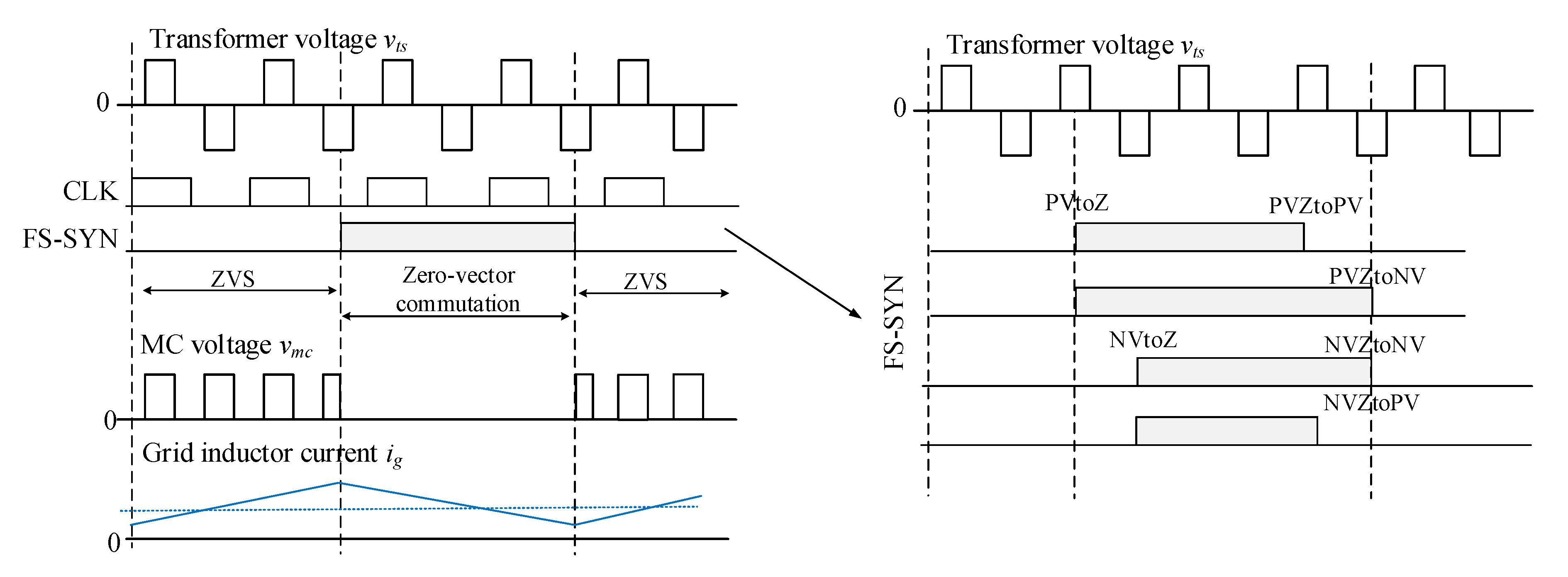
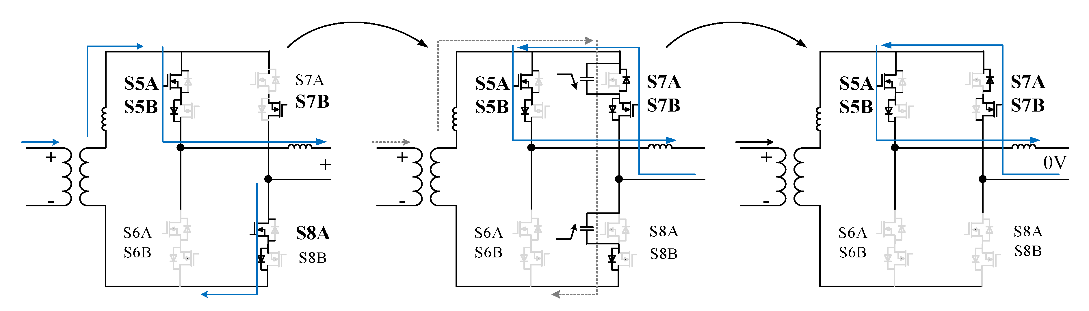
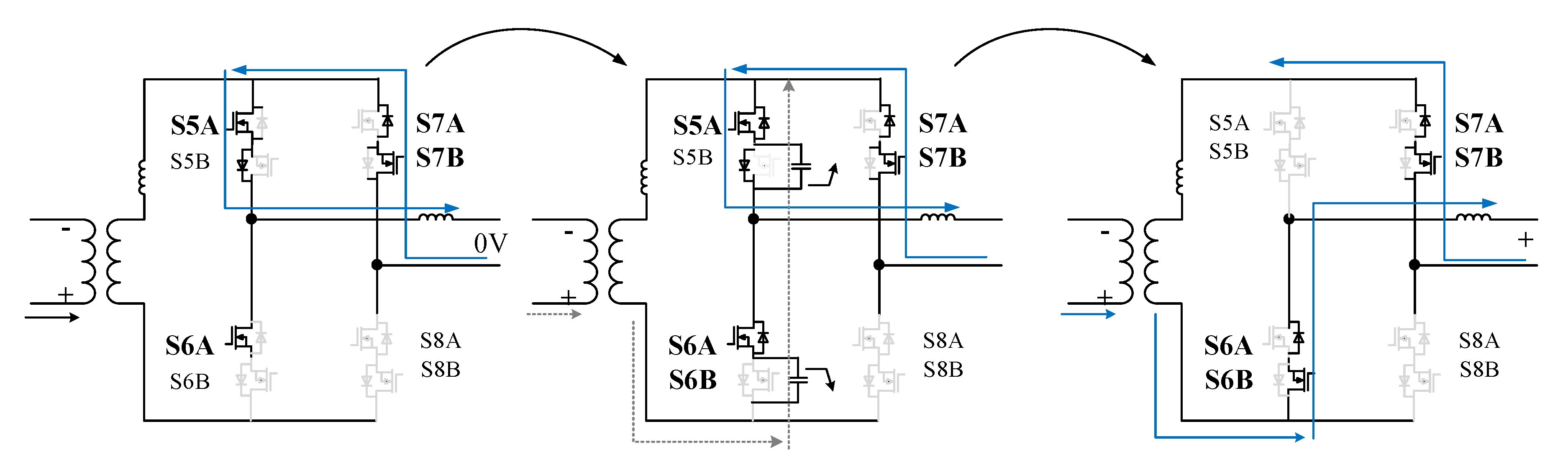
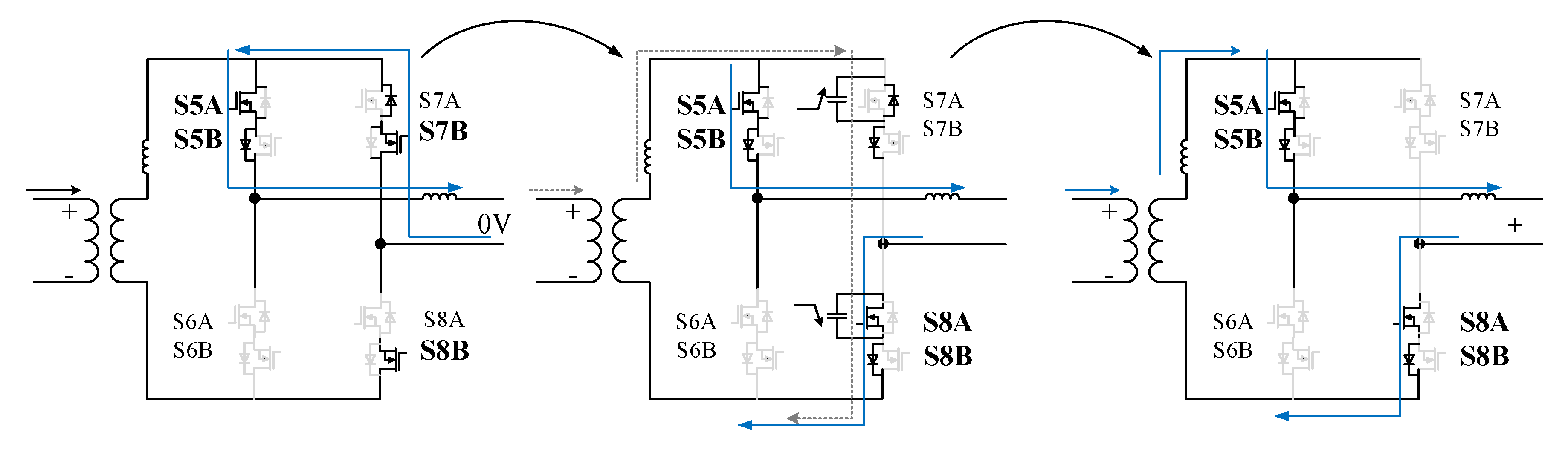
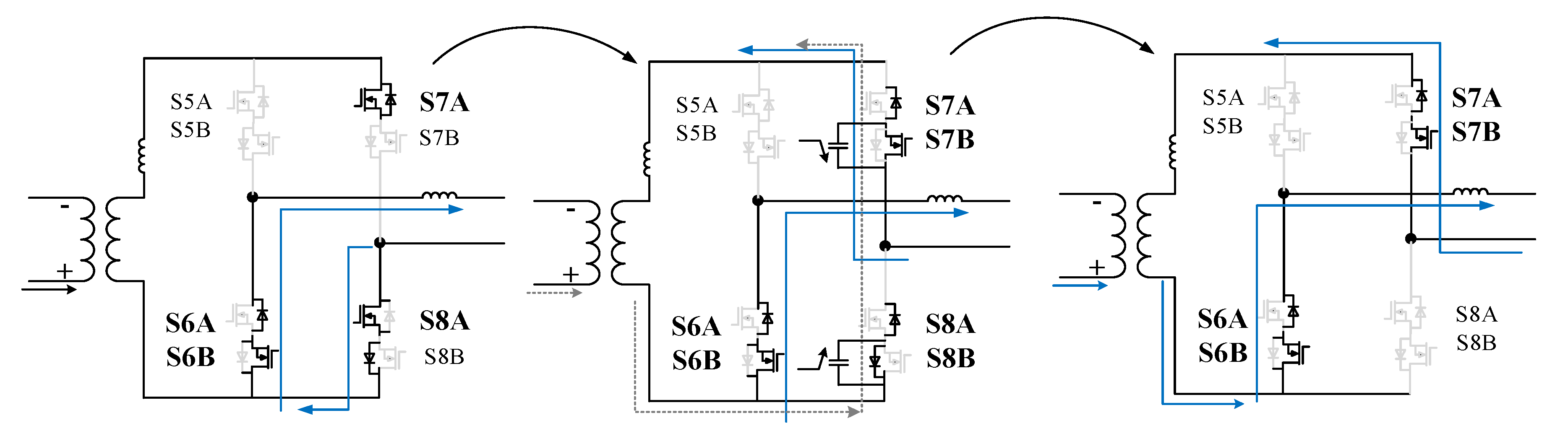
3.3. Carrier Comparison with Zero-Vector Commutation
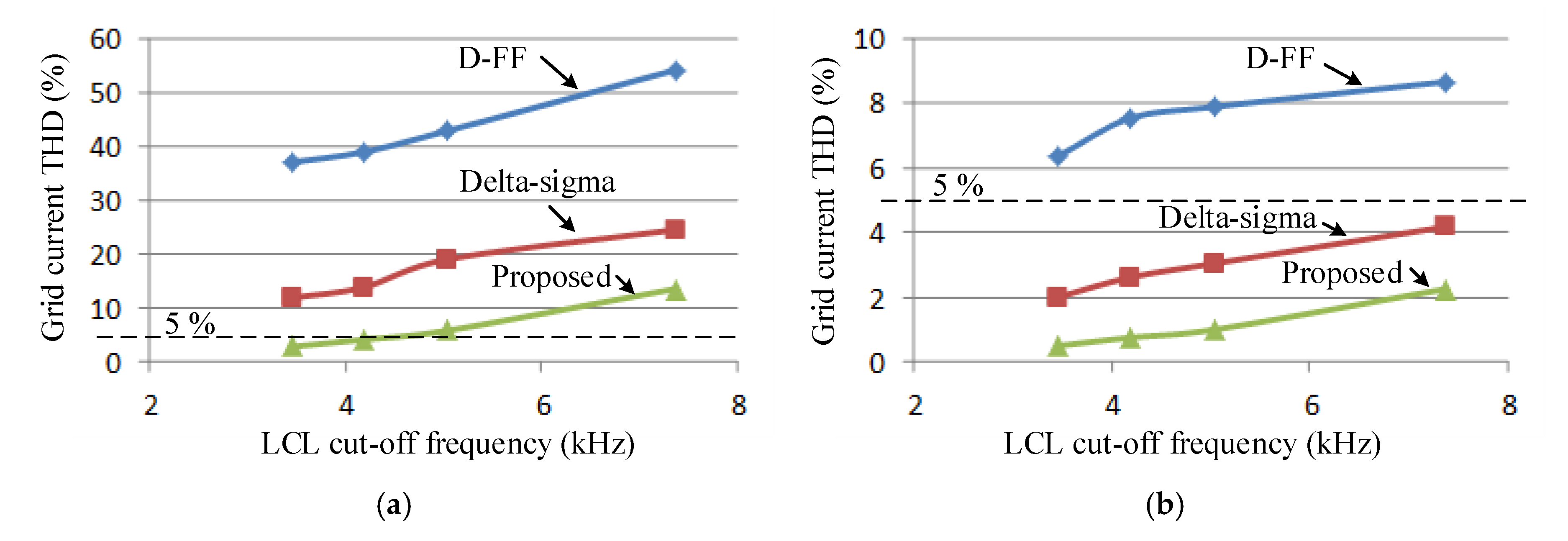
4. Simulation Results
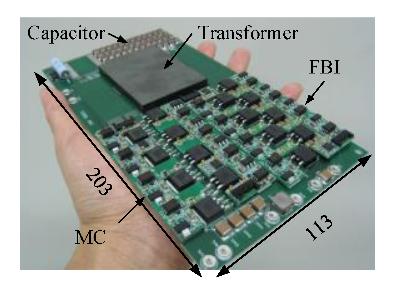
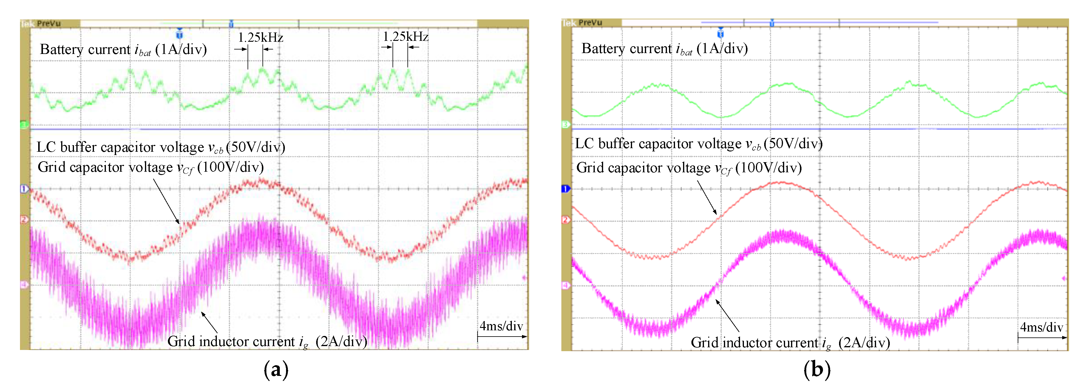
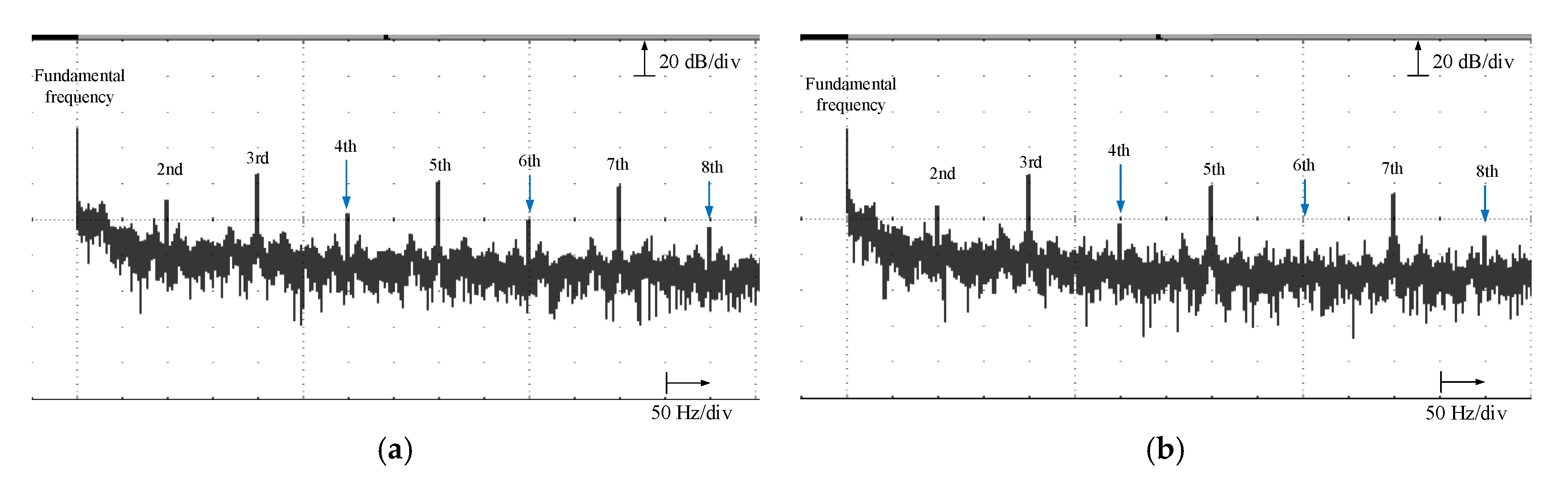
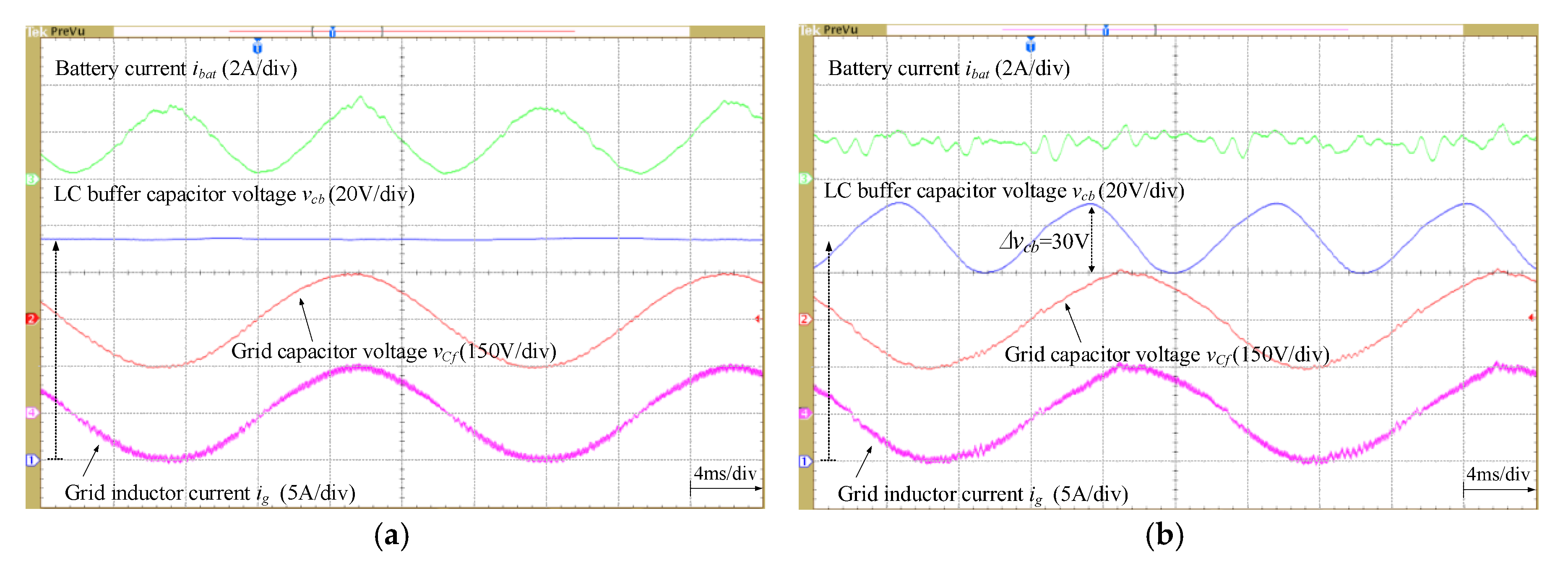
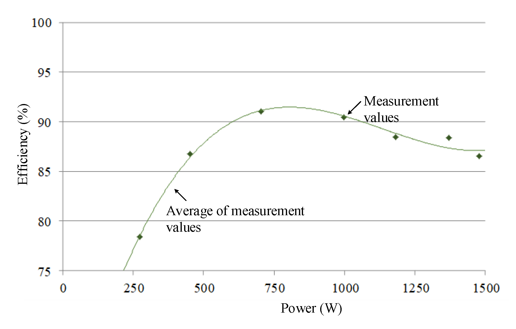
5. Experimental Results
6. Conclusions
Author Contributions
Funding
Conflicts of Interest
References
- Raggl, K.; Nussbaumer, T.; Doerig, G.; Biela, J.; Kolar, J.W. Comprehensive design and optimization of a high-power density single-phase PFC. IEEE Trans. Ind. Electron. 2009, 56, 2574–2587. [Google Scholar] [CrossRef]
- Choi, W.; Rho, K.-M.; Cho, B.-H. Fundamental duty modulation of dual-active bridge converter for wide-range operation. IEEE Trans. Power Electron. 2016, 31, 4048–4606. [Google Scholar] [CrossRef]
- Jovanovic, M.M.; Jang, Y. State-of-the art, single-phase, active power factor correction techniques for high power applications. IEEE Trans. Ind. Electron. 2009, 56, 2574–2587. [Google Scholar] [CrossRef]
- Musavi, F.; Eberle, W.; Dunford, W.G. A high-performance single-phase bridgeless interleaved PFC converter for plug-in hybrid electric vehicle battery chargers. IEEE Trans. Ind. Appl. 2011, 47, 1833–1843. [Google Scholar] [CrossRef]
- Xue, L.; Shen, Z.; Boroyevich, D.; Mattavelli, P. GaN-based high frequency totem-pole bridgeless PFC design with digital implementation. In Proceedings of the IEEE Applied Power Electronics Conference and Exposition (APEC), Charlotte, NC, USA, 15–19 March 2015; pp. 759–766. [Google Scholar]
- Kolar, J.W.; Friedli, T.; Rodriguez, J.; Wheeler, P.W. Review of three-phase PWM AC-AC converter topologies. IEEE Trans. Ind. Electron. 2011, 58, 11. [Google Scholar] [CrossRef]
- Empringham, L.; Kolar, J.W.; Rodrigues, J.; Wheeler, P.W.; Clare, J.C. Technological issues and industrial application of matrix converters: A review. IEEE Trans. Ind. Electron. 2013, 60, 10. [Google Scholar] [CrossRef]
- Sun, Y.; Liu, Y.; Su, M.; Xiong, W.; Yang, J. Review of active power decoupling topologies in single-phase systems. IEEE Trans. Power Electron. 2016, 31, 4778–4794. [Google Scholar] [CrossRef]
- Komeda, S.; Fujita, H. A power decoupling control method for an isolated sing-phase AC-to-DC converter based on direct AC-to-AC converter topology. IEEE Trans. Power Electron. 2018, 33, 9691–9698. [Google Scholar] [CrossRef]
- Itoh, J.-I.; Hayashi, F. ripple current reduction of a fuel cell for a single-phase isolated converter using a DC active filter with a center tap. IEEE Trans. Power Electron. 2009, 25, 550–556. [Google Scholar] [CrossRef]
- Takaoka, N.; Takahashi, H.; Itoh, J.-I. Isolated single-phase matrix converter using center-tapped transformer for power decoupling capability. IEEE Trans. Ind. Appl. 2018, 54, 1523–1531. [Google Scholar] [CrossRef]
- Wang, M.; Huang, Q.; Yu, W.; Huang, A.Q. An isolated bi-directional soft-switched DC-AC converter using wide-band-gap devices with novel carrier-based unipolar modulation technique under synchronous rectification. In Proceedings of the IEEE Applied Power Electronics Conference and Exposition (APEC), Charlotte, NC, USA, 15–19 March 2015; pp. 2317–2324. [Google Scholar]
- Varajao, D.; Rui, E.A.; Miranda, L.M.; Lopes, J.A.P.; Weise, N. Control of an isolated sing-phase bidirectional AC-DC matric converter for V2G applications. Electr. Power Syst. Res. 2017, 149, 19–29. [Google Scholar] [CrossRef]
- Norrga, S. Experimental study of a soft-switched isolated bidirectional AC-DC converter without auxiliary circuit. IEEE Trans. Power Electron. 2006, 21, 6. [Google Scholar] [CrossRef]
- Nakata, Y.; Orikawa, K.; Itoh, J.-I. Several-hundred-kHz single-phase to commercial frequency three-phase matrix converter using Delta-sigma modulation with space vector. In Proceedings of the IEEE Energy Conversion Congress and Exposition (ECCE), Pittsburg, PA, USA, 14–18 September 2014; pp. 571–578. [Google Scholar]
- Takaoka, N.; Takahashi, H.; Itoh, J.-I.; Chiang, G.T.; Sugiyama, T.; Sugai, M. Power decoupling method comparison of isolated single-phase matrix converters using center-tapped transformer with PDM. In Proceedings of the IEEE Energy Conversion Congress and Exposition (ECCE), Montreal, QC, Canada, 20–24 September 2015. [Google Scholar]
- Chiang, G.T.; Takahide, S.; Masaru, S. Optimal design of a matrix converter with a LC active buffer to onboard vehicle battery charger in single phase grid structure. In Proceedings of the 18th European Conference on Power Electronics and Applications, Karlsruhe, Germany, 5–9 September 2016. [Google Scholar]
- He, J.; Li, Y.W. Hybrid voltage and current control approach for DG grid interfacing converters with LCL filters. IEEE Trans. Ind. Electron. 2013, 60, 1797–1809. [Google Scholar] [CrossRef]
- She, H.; Lin, H.; He, B.; Wang, X.; Yue, L.; An, X. Implementation of voltage-based commutation in space-vector modulated matrix converter. IEEE Trans. Ind. Electron. 2012, 59, 154–166. [Google Scholar]
- Afsharian, J.; Xu, D.; Wu, B.; Gong, B.; Yang, Z. A new PWM and commutation scheme for one phase loss operation of three-phase isolated buck matrix-type rectifier. IEEE Trans. Power Electron. 2018, 33, 9854–9865. [Google Scholar] [CrossRef]


| Symbols | Polarity = 1 | Polarity = 0 | ||||
|---|---|---|---|---|---|---|
| SPQ | 1 | 1 | 1 | 0 | 0 | 0 |
| SNQ | 0 | 0 | 1 | 1 | 1 | 1 |
| Vts | + | - | +/− | + | - | +/− |
| S5 | 1 | 0 | 0 | 0 | 1 | 1 |
| S6 | 0 | 1 | 1 | 1 | 0 | 0 |
| S7 | 0 | 1 | 0 | 1 | 0 | 1 |
| S8 | 1 | 0 | 1 | 0 | 1 | 0 |
| Vmc | + | + | 0 | - | - | 0 |
| Actions | PV-to-Z | PVZ-to-PV | PVZ-to-NV | NV-to-Z | NVZ-to-PV | NVZ-to-NV | ||||||
|---|---|---|---|---|---|---|---|---|---|---|---|---|
| Sequence | 1st | 2nd | 1st | 2nd | 1st | 2nd | 1st | 2nd | 1st | 2nd | 1st | 2nd |
| S5A | 1 | 1 | 1 | 1 | 1 | 0 | 0 | 0 | 1 | 1 | 0 | 0 |
| S5B | 1 | 1 | 1 | 1 | 0 | 0 | 0 | 0 | 0 | 1 | 0 | 0 |
| S6A | 0 | 0 | 0 | 0 | 1 | 1 | 1 | 1 | 0 | 0 | 1 | 1 |
| S6B | 0 | 0 | 0 | 0 | 0 | 1 | 1 | 1 | 1 | 0 | 1 | 1 |
| S7A | 0 | 1 | 0 | 0 | 1 | 1 | 0 | 0 | 0 | 0 | 1 | 1 |
| S7B | 1 | 1 | 1 | 0 | 1 | 1 | 1 | 0 | 0 | 0 | 0 | 1 |
| S8A | 1 | 0 | 0 | 1 | 0 | 0 | 1 | 1 | 1 | 1 | 1 | 0 |
| S8B | 0 | 0 | 1 | 1 | 0 | 0 | 0 | 1 | 1 | 1 | 0 | 0 |
| Names | Symbol | Value |
|---|---|---|
| Battery voltage | vbat | 100–200 V |
| Grid voltage | vac | 100 V 50 Hz |
| Transformer voltage ratio | Nfbi:Nmc | 1:1.75 |
| FBI switching frequency | fsw_fbi | 100 kHz |
| Capacitor | Cb | 400 μF |
| Inductor | Lb | 10 μH |
| MC switching frequency | fsw_mc | 10 kHz |
| Filter inductor | Lf | 50 μH |
| Filter capacitor | Cf | 22 μF |
| Grid inductor | Lg | 425 μH |
| Modulation Methods | Power Decoupling | Control Complexity | Quality Waveform (Grid Current THD, Battery Current Ripple) | LCL Filter Sizing | |
|---|---|---|---|---|---|
| Low-Power | High-Power | ||||
| SPWM synchronous rec. [12] | × | △ | 〇 | 〇 | 50 kHz Lf: 10 μH Cf:1 μF |
| PWM four-step comm. [13] | × | × | 〇 | 〇 | 5 kHz Lf: 300 μH Cf:4.7 μF |
| PWM comm. [14] | × | × | △ | 〇 | N/A |
| D-FF [15] | 〇 | 〇 | × | △ | × 3 kHz Lf: 100 μH Cf:22 μF |
| Delta-sigma [16] | 〇 | △ | △ | 〇 | △ 2 kHz Lf: 100 μH Cf: 45 μF |
| Zero-vector commutation | 〇 | △ | 〇 | 〇 | 〇 5 kHz Lf: 50 μH Cf:22 μF |
© 2020 by the authors. Licensee MDPI, Basel, Switzerland. This article is an open access article distributed under the terms and conditions of the Creative Commons Attribution (CC BY) license (http://creativecommons.org/licenses/by/4.0/).
Share and Cite
Teck Chiang, G.; Sugiyama, T. Methods of Modulation for Current-Source Single-Phase Isolated Matrix Converter in a Grid-Connected Battery Application. Energies 2020, 13, 3845. https://doi.org/10.3390/en13153845
Teck Chiang G, Sugiyama T. Methods of Modulation for Current-Source Single-Phase Isolated Matrix Converter in a Grid-Connected Battery Application. Energies. 2020; 13(15):3845. https://doi.org/10.3390/en13153845
Chicago/Turabian StyleTeck Chiang, Goh, and Takahide Sugiyama. 2020. "Methods of Modulation for Current-Source Single-Phase Isolated Matrix Converter in a Grid-Connected Battery Application" Energies 13, no. 15: 3845. https://doi.org/10.3390/en13153845
APA StyleTeck Chiang, G., & Sugiyama, T. (2020). Methods of Modulation for Current-Source Single-Phase Isolated Matrix Converter in a Grid-Connected Battery Application. Energies, 13(15), 3845. https://doi.org/10.3390/en13153845