Wide-Supply-Voltage-Range CMOS Bandgap Reference for In Vivo Wireless Power Telemetry


Abstract
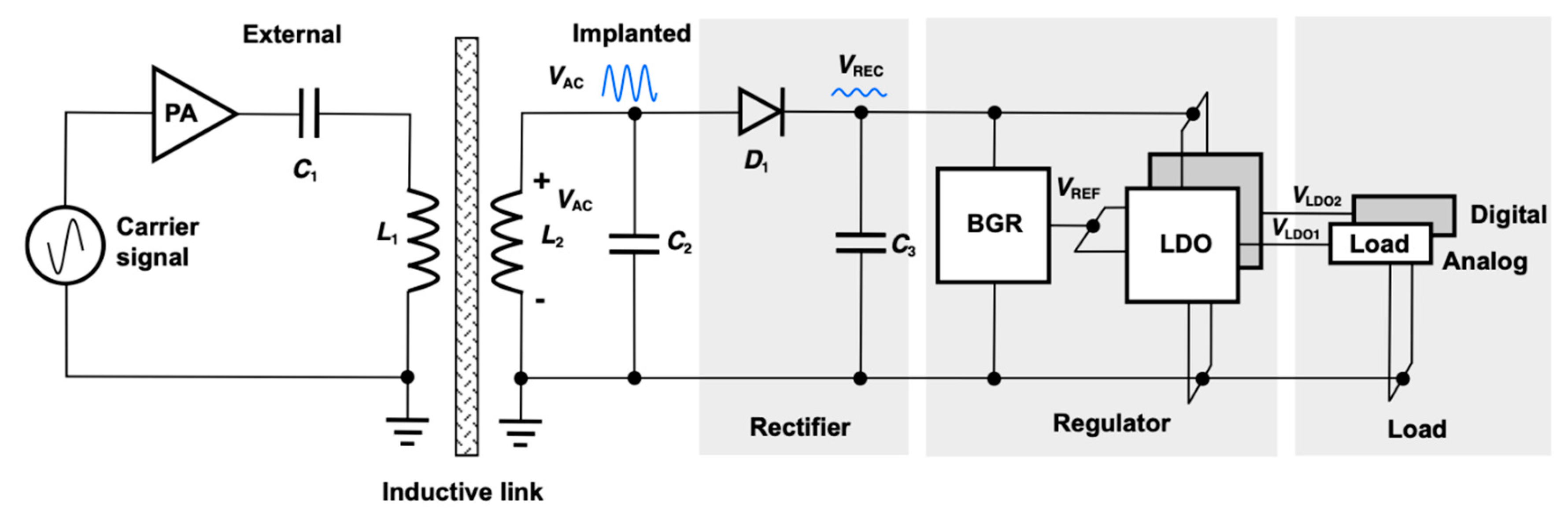
1. Introduction
2. Architecture of the BGR Circuit
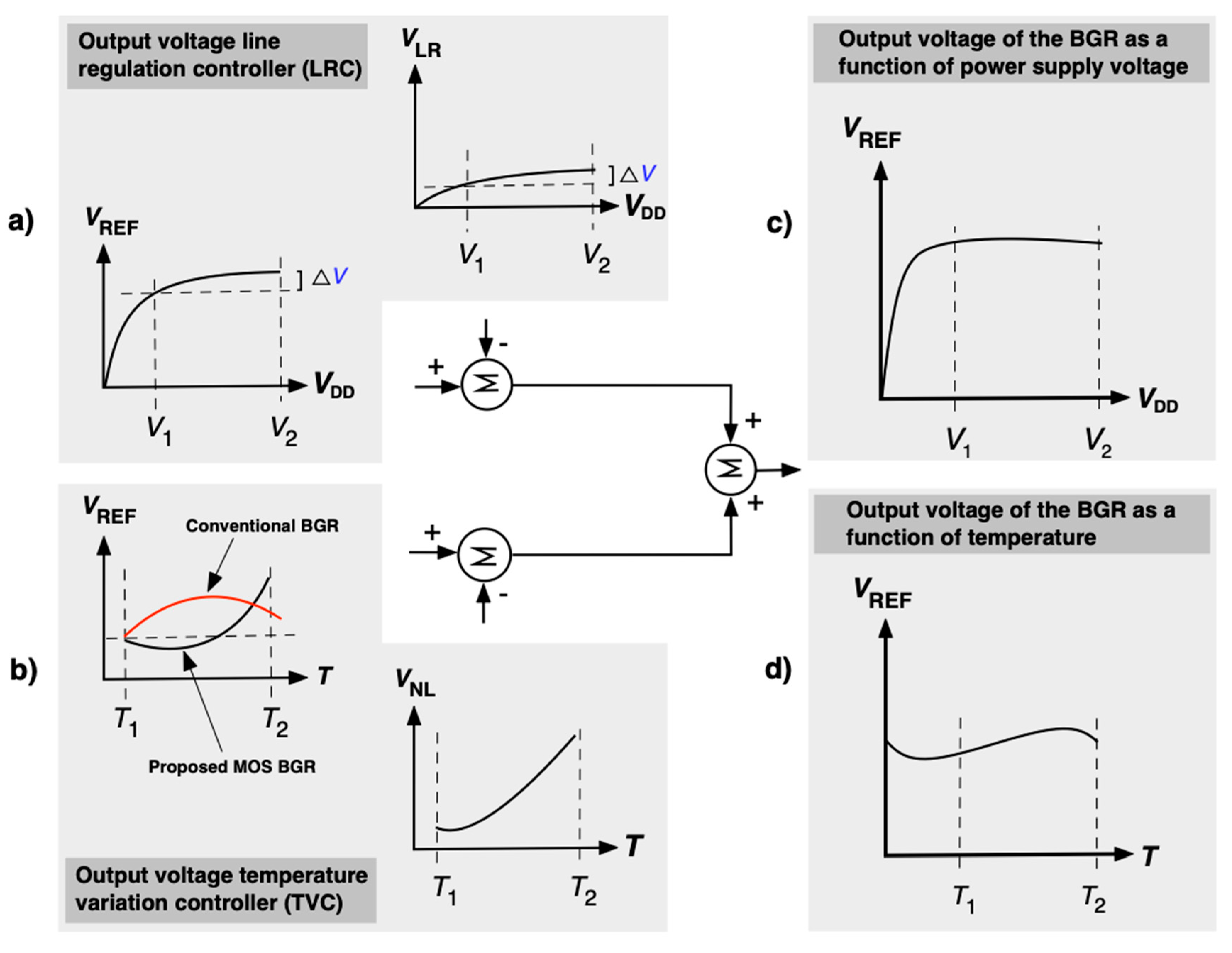
2.1. Conventional BGR Scheme
2.2. Proposed BGR
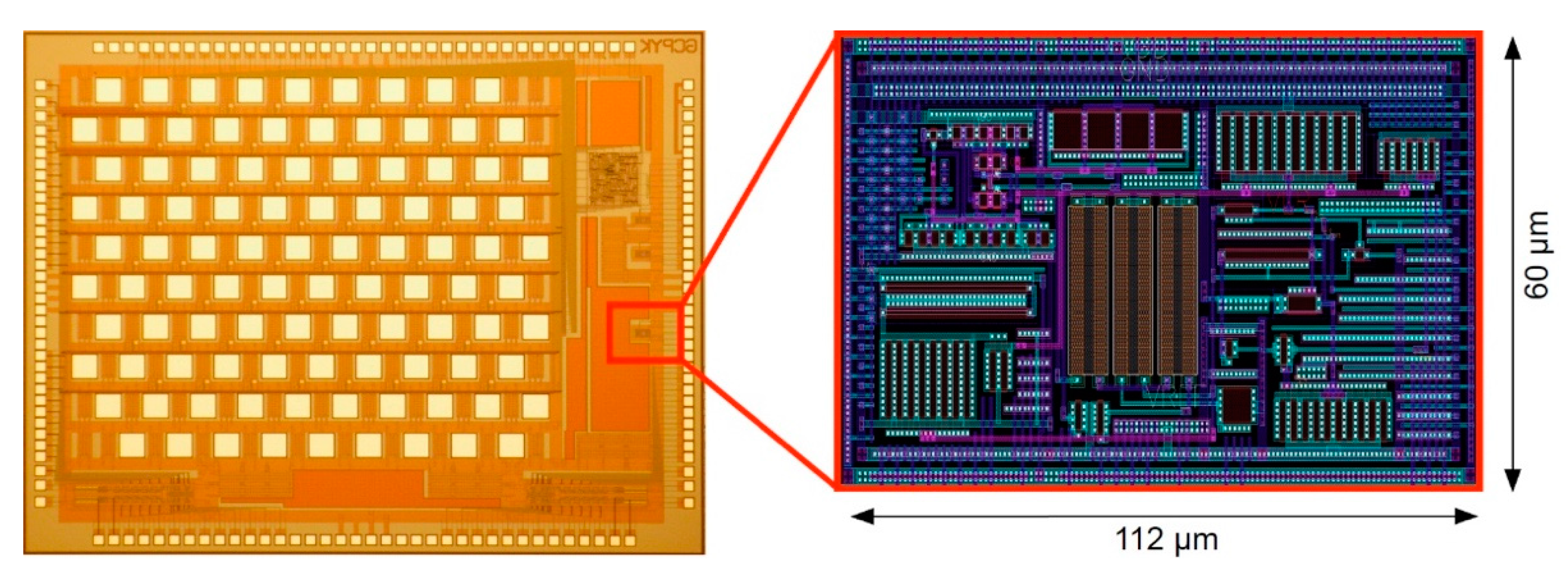
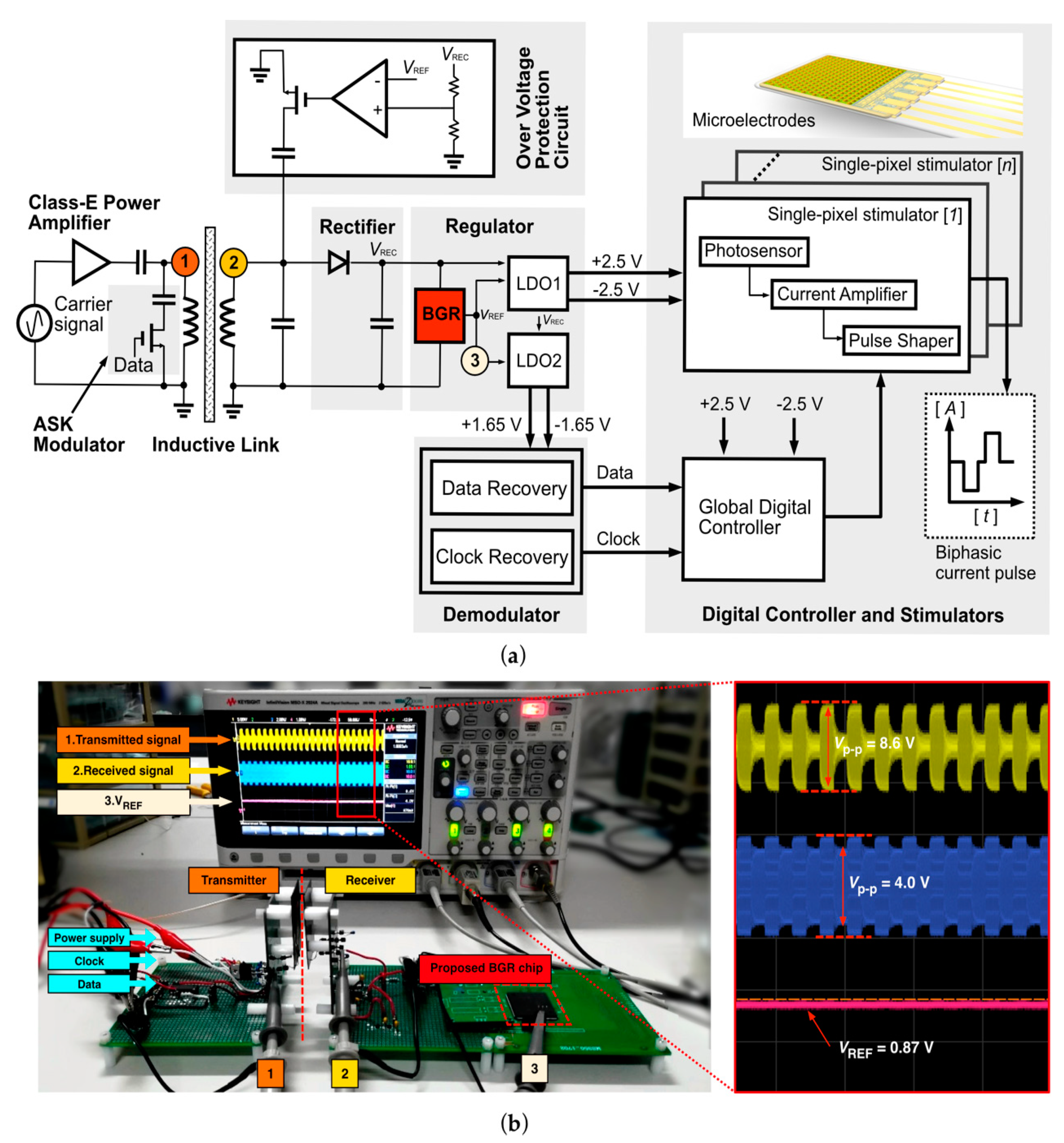
3. Simulation and Experimental Results
4. Conclusions
Author Contributions
Funding
Acknowledgments
Conflicts of Interest
Appendix A
Appendix B

References
- Ritter, R.; Handwerker, J.; Liu, T.; Ortmanns, M. Telemetry for Implantable Medical Devices: Part 1—Media Properties and Standards. IEEE Solid-State Circuits Mag. 2014, 6, 47–51. [Google Scholar] [CrossRef]
- Kang, H.; Abbasi, W.H.; Kim, S.; Kim, J. Fully Integrated Light-Sensing Stimulator Design for Subretinal Implants. Sensors 2019, 19, 536. [Google Scholar] [CrossRef] [PubMed]
- Tokuda, T.; Takeuchi, Y.; Sagawa, Y.; Noda, T.; Sasagawa, K.; Nishida, K.; Ohta, J. Development and in vivo Demonstration of CMOS-Based Multichip Retinal Stimulator with Simultaneous Multisite Stimulation Capability. IEEE Trans. Biomed. Circuits Syst. 2010, 4, 445–453. [Google Scholar] [CrossRef] [PubMed]
- Ayton, L.N.; Blamey, P.J.; Guymer, R.H.; Luu, C.D. First-in-Human Trial of a Novel Suprachoroidal Retinal Prosthesis. PLoS ONE 2014, 9, e115239. [Google Scholar] [CrossRef] [PubMed]
- Kofman, K.E.; Buckley, T.; McGrouther, D.A. Complications of transcutaneous metal devices. Eur. J. Plast. Surg. 2012, 35, 673–682. [Google Scholar] [CrossRef] [PubMed][Green Version]
- Kuo, P.-H.; Wong, O.-Y.; Tzeng, C.-K.; Wu, P.-W.; Chiao, C.-C.; Chen, P.-H.; Chen, P.-C.; Tsai, Y.-C.; Chu, F.-L.; Ohta, J.; et al. Improved Charge Pump Design and Ex Vivo Experimental Validation of CMOS 256-Pixel Photovoltaic-Powered Subretinal Prosthetic Chip. IEEE Trans. Biomed. Eng. 2019, 67, 1490–1504. [Google Scholar] [CrossRef] [PubMed]
- Pixium Vision S A. 2001. Available online: http://pixium-vision.com (accessed on 1 April 2020).
- Lee, B.; Kiani, M.; Ghovanloo, M. A Triple-Loop Inductive Power Transmission System for Biomedical Applications. IEEE Trans. Biomed. Circuits Syst. 2016, 10, 138–148. [Google Scholar] [CrossRef] [PubMed]
- Jegadeesan, R.; Nag, S.; Agarwal, K.; Member, S. Enabling Wireless Powering and Telemetry for Peripheral Nerve Implants. IEEE J. Biomed. Health Inform. 2015, 19, 958–970. [Google Scholar] [CrossRef] [PubMed]
- Lo, Y.; Chen, K.; Gad, P.; Liu, W. An On-Chip Multi-Voltage Power Converter with Leakage Current Prevention Using 0.18 µm High-Voltage CMOS Process. IEEE Trans. Biomed. Circuits Syst. 2016, 10, 163–174. [Google Scholar] [CrossRef] [PubMed]
- Hu, Y.; Gervais, J.F.; Sawan, M. High power efficiency inductive link with full-duplex data communication. Proc. IEEE Int. Conf. Electron. Circuits Syst. 2002, 1, 359–362. [Google Scholar] [CrossRef]
- Ha, S.; Khraiche, M.L.; Akinin, A.; Jing, Y.; Damle, S.; Kuang, Y.; Bauchner, S.; Lo, Y.H.; Freeman, W.R.; Silva, G.A.; et al. Towards high-resolution retinal prostheses with direct optical addressing and inductive telemetry. J. Neural Eng. 2016, 13, 1–19. [Google Scholar] [CrossRef] [PubMed]
- Tzschoppe, C.; Jörges, U.; Richter, A.; Lindner, B.; Ellinger, F. Theory and Design of Advanced CMOS Current Mirrors. In Proceedings of the 2015 SBMO/IEEE MTT-S International Microwave and Optoelectronics Conference (IMOC), Porto de Galinhas, Brazil, 3–6 November 2015; pp. 1–5. [Google Scholar] [CrossRef]
- Kim, J.; Basham, E.; Pedrotti, K.D. Geometry-based optimization of radio-frequency coils for powering neuroprosthetic implants. Med. Biol. Eng. Comput. 2013, 51, 123–134. [Google Scholar] [CrossRef] [PubMed]
- Razavi, B. Design of Analog CMOS Integrated Circuit, 2nd ed.; McGraw-Hill Education: New York, NY, USA, 2017. [Google Scholar]
- Adeeb, M.A.; Islam, A.B.; Haider, M.R.; Tulip, F.S.; Ericson, M.N.; Islam, S.K. An inductive link-based wireless power transfer system for biomedical applications. Act. Passiv. Electron. Compon. 2012, 2012, 879294. [Google Scholar] [CrossRef]
- Osaki, Y.; Hirose, T.; Kuroki, N.; Numa, M. 1.2-V Supply, 100-nW, 1.09-V Bandgap and 0.7-V Supply, 52.5-nW, 0.55-V Sub-bandgap Reference Circuits for Nanowatt CMOS LSIs. IEEE J. Solid-State Circuits 2013, 48, 1530–1538. [Google Scholar] [CrossRef]
- Ma, B.; Yu, F. A Novel 1.2–V 4.5-ppm/°C Curvature-Compensated CMOS Bandgap Reference. IEEE Trans. Circuits Syst. I Regul. Pap. 2014, 61, 1026–1035. [Google Scholar] [CrossRef]
- Becker-Gomez, A.; Lakshmi Viswanathan, T.; Viswanathan, T.R. A Low-Supply-Voltage CMOS Sub-Bandgap Reference. IEEE Trans. Circuits Syst. II Express Briefs 2008, 55, 609–613. [Google Scholar] [CrossRef]
- Duan, Q.; Roh, J.; Member, S. A 1.2-V 4.2-ppm C High-Order Curvature- Compensated CMOS Bandgap Reference. IEEE Trans. Circuits Syst. I Regul. Pap. 2015, 62, 662–670. [Google Scholar] [CrossRef]
- Mattia, O.E.; Klimach, H.; Bampi, S. Resistorless BJT bias and curvature compensation circuit at 3.4 nW for CMOS bandgap voltage references. Electron. Lett. 2014, 50, 863–864. [Google Scholar] [CrossRef]
- Gray, P.; Meyer, R. Analysis and Design of Analog Integrated Circuits, 5th ed.; John Wiley and Sons: Hoboken, NJ, USA, 2010. [Google Scholar]
- Tsividis, Y.P.; Ulmer, R.W. A CMOS Voltage Reference. IEEE J. Solid-State Circuits 1978, 13, 774–778. [Google Scholar] [CrossRef]
- Pelgrom, M.J.M.; Duinmaijer, A.C.J.; Welbers, A.P.G. Matching properties of MOS transistors. IEEE J. Solid-State Circuits 1989, 24, 1433–1439. [Google Scholar] [CrossRef]


| Component | Parameter | Component | Parameter |
|---|---|---|---|
| MP1, MP2 | W = 10 µm, L = 5 µm | MN1, MN2, MN3 | W = 3.5 µm, L = 1 µm |
| MP3 | W = 20 µm, L = 1 µm | MN4 | W = 50 µm, L = 1 µm |
| MP4 | W = 2 µm, L = 5 µm | MN5 | W = 2 µm, L = 1 µm |
| MP5 | W = 50 µm, L = 1 µm | MN6 | W = 0.9 µm, L = 1 µm |
| MP6 | W = 5 µm, L = 1 µm | MN7 | W = 80 µm, L = 1 µm |
| MP7 | W = 1 µm, L = 25 µm | MN8 | W = 10 µm, L = 1 µm |
| MP8 | W = 25 µm, L = 1 µm | R1 | 40 kΩ |
| MP9 | W = 1 µm, L = 1.5 µm | R2 | 20 kΩ |
| Parameter | This Work | [18] | [19] |
|---|---|---|---|
| Technology | CMOS 0.35 µm | CMOS 0.18 µm | CMOS 0.18 µm |
| Supply voltage (V) | 3.3 | 1.2 | 1.4 |
| Line regulation | 1.85 mV/V (2.3–5 V) 0.4 mV/V (2.5–13 V) 1 | 0.054%/V (1.2–2) | ±0.3 mV (1.1–1.8) |
| PSRR (dB) | −54 | −84 | −75 |
| TC (ppm/°C) | 11.9 | 3.4 | 4 |
| Active area (mm2) | 0.0067 | 0.036 | - |
© 2020 by the authors. Licensee MDPI, Basel, Switzerland. This article is an open access article distributed under the terms and conditions of the Creative Commons Attribution (CC BY) license (http://creativecommons.org/licenses/by/4.0/).
Share and Cite
Zawawi, R.B.A.; Abbasi, W.H.; Kim, S.-H.; Choi, H.; Kim, J. Wide-Supply-Voltage-Range CMOS Bandgap Reference for In Vivo Wireless Power Telemetry. Energies 2020, 13, 2986. https://doi.org/10.3390/en13112986
Zawawi RBA, Abbasi WH, Kim S-H, Choi H, Kim J. Wide-Supply-Voltage-Range CMOS Bandgap Reference for In Vivo Wireless Power Telemetry. Energies. 2020; 13(11):2986. https://doi.org/10.3390/en13112986
Chicago/Turabian StyleZawawi, Ruhaifi Bin Abdullah, Wajahat H. Abbasi, Seung-Hwan Kim, Hojong Choi, and Jungsuk Kim. 2020. "Wide-Supply-Voltage-Range CMOS Bandgap Reference for In Vivo Wireless Power Telemetry" Energies 13, no. 11: 2986. https://doi.org/10.3390/en13112986
APA StyleZawawi, R. B. A., Abbasi, W. H., Kim, S.-H., Choi, H., & Kim, J. (2020). Wide-Supply-Voltage-Range CMOS Bandgap Reference for In Vivo Wireless Power Telemetry. Energies, 13(11), 2986. https://doi.org/10.3390/en13112986