Article

Thermo-Fluidic Characterizations of Multi-Port Compact Thermal Model of Ball-Grid-Array Electronic Package

1
Thales Corporate Engineering, 19-21 Avenue Morane Saulnier, 78140 Vélizy-Villacoublay, France
2
LMEE, Université d’Evry, Université Paris-Saclay, 91020 Evry, France
*
Author to whom correspondence should be addressed.
Energies 2020, 13(11), 2968; https://doi.org/10.3390/en13112968
Submission received: 31 March 2020 / Revised: 20 May 2020 / Accepted: 3 June 2020 / Published: 9 June 2020
(This article belongs to the Special Issue Thermal and Electro-thermal System Simulation 2020)

Abstract

:
The concept of a single-input/multi-output thermal network was proposed by the Development of Libraries of Physical models for an Integrated design environment (DELPHI) consortium more than twenty years ago. The present work highlights the recent improvements made to efficiently derive a low-computing-effort model from a fully detailed numerical model and to characterize its performances. The temperature predictions of a deduced ball-grid-array (BGA) dynamic compact thermal model are compared to those of a realistic three-dimensional representation, including the large set of internal copper traces, as well as its board structure, which has been validated by experiment. The current study discloses a method for creating an amalgam reduced-order modal model (AROMM) for that electronic component family that allows the preservation of the geometry integrity and shortening scenarios computation. Typically, the AROMM method reduces by a factor of 600 the computation time needed to obtain the solution while keeping the error on the maximum temperature below 2%. Then, a meta-heuristic optimization is run to derive a more practical low-order resistor capacitor model that enables a thermo-fluidic analysis at the board level. Based on the calibrated numerical model, a novel AROMM method was investigated in order to address the chip behavior submitted to multiple heat sources. The first results highlight the capability to enforce a non-uniform power distribution on the upper surface of the silicon chip. Thus, the chip design layout can be analyzed and optimized to prevent thermal and reliability issues.

1. Introduction

The thermal behavior of electronic components can be finely predicted by thermal and fluidic numerical simulations [1]. However, as the geometrical and functional description of the component grows in complexity, the time needed for simulations becomes unbearable for parametric studies if fully detailed numerical representations are used.
To overcome the inherent time-consuming computation of such a detailed model, new methods for creating surrogate models able to properly reproduce its steady-state response, as well as transient ones, in a shorter time, were developed. This statement leads research, at first, toward dynamic compact thermal models (DCTMs) [2], which aim to predict the key thermal characteristics of a component. The Development of Libraries of Physical models for an Integrated design environment (DELPHI) approach promotes the use of a matrix of thermal resistances that link the sub-divided exterior surfaces of a component to its junction, which is the highest temperature of the component. The construction of a DCTM required training data, obtained by numerical simulations or experiment results.
Modal models are an alternative to DTCMs. They can be seen as an extension of the classical Fourier decomposition. The temperature is searched as a sum of known elementary spatial functions, called the modes, weighted by unknown coefficients. Different methods are based on this principle: The most popular is the proper orthogonal decomposition method (POD), which requires knowledge of thermal fields from experimental or numerical data [3,4]. However, the challenge is to find a modal base independent of boundary conditions. In that perspective, Codecasa et al. used a multi-point moment-matching method algorithm [5]. Joly et al. [6] used ‘branch modes’ to solve problems associated with time-dependent boundary conditions. The originality of the branch modes is that ‘the branch eigenvalue problem’ uses Steklov boundary conditions. This method has been extended to the amalgam reduced-order modal model (AROMM) method: A modal base is calculated by solving an eigenvalue problem. The reduced model is obtained by reducing the initial base by the amalgam method [7]. These developments gave birth to a new hybrid methodology to build DELPHI-inspired DCTMs by replacing the full detailed models by a reduced-order model based on the modal approach [8,9].
However, more complex configurations demand more sophisticated methods, in which simple reduced models are built and then connected to each other. Following that idea, Grosjean et al. developed a substructuring modal method that allows the reduction of an electronic board with several active components [10,11]. Codecasa et al. also coupled boundary-independent reduced models of components [12]. However, in those studies, the elementary components were simple (Quad Flat No-leads (QFN) package 16 or 32 with a single heat source, or Insulated Gate Bipolar Transistor (IGBT) with heat sources activated together), as the challenge was to couple those independent reduced models efficiently.
A single component with independent multiple heat sources has also been recently considered using the MPMM method [9] or AROMM [13]. Those studies have been limited to a component with a couple of independent sources. The objective of this paper is to present a reduced modal model of a ball grid array package with nine independent heat sources located on the top of the chip.
The paper is organized as follows. The position of the problem, as well as the studied material, is presented first. Then, the experimental setup and measurements are introduced. In the second step, the numerical model is built and experimentally validated for different environments when a uniform power distribution is localized on top of the chip. The creation of the reduced-order model by the modal method is then presented, and two different use cases are outlined. The first use case highlights how reduced-order modal models can be used to replace the detailed model for the creation of the boundary condition-independent dynamic compact thermal model. The second one presents a purely numerical study in which the power distribution is not uniformly applied on the top surface of the chip and demonstrates the relevance of this approach applied to this complex configuration.

2. Position of the Problem

The ball grid array package with 208 solder balls is a very popular package for integrated circuits (IC) with a large interconnection number. That kind of IC package usually consists of an active centered semiconductor chip that is glued on a two-copper-layer laminate, as described in Figure 1.
The semiconductor chip, as well as its gold wire bonds, is over-molded with a plastic resin. The diameter of the gold wires is 25.4 µm, which highlights the aspect ratio constraints.
The laminate structure routes functional signals from the input/output of the chip to the solder balls and also acts as a radiator for heat spreading. It is made up by two thin signal layers interconnected by vias. Figure 2 shows the copper patterns of the three layers of the studied ball-grid-array (BGA) substrate.
Table 1 supplies the thermal properties used to establish the numerical model of this BGA package.

3. Experimental Measurements

3.1. Experimental Setup

The complex component package cannot be tested independently of a printed circuit board (PCB). Thus, a set of standardized tests [14] was performed for two standardized PCBs, named 2s0p [15] and 2s2p [16], as well as for various stabilized airflow boundary conditions (still air [17] and forced moving air [18]) in order to check the component thermal performances according to JEDEC recommendations.
Figure 3 shows the stack-up of seven layers that alternate between high- (1, 3, 5, 7) and very-low (2, 4, 6)-conductivity layers that are defined for a JEDEC 2s2p thermal test board.
The “s” refers to the signal layers and “p” to the buried power (or ground plane) layers. The two internal quasi full-covered copper layers act as efficient in-plane heat spreaders. The overall length, width, and thickness of the test board are respectively 102, 112, and 1.6 mm. The typical width of a copper trace is 300 µm.

3.2. Measurements

Experimental measurements have been performed by the thermal test services of Analysis Tech following all JEDEC n° 51 requirements. Figure 4 displays the standardized experimental setup used to characterize this BGA208.
Following JEDEC standards, the chip behavior is characterized by a metric, which is called junction-to-ambient thermal resistance, defined by Equation (1):
R J A ( Q ) = [ T J T ] / Q
That metric indicates the flowing capacity of a uniform power ( Q ) dissipated in the device through all the thermal paths between the chip junction ( T J ) and the ambient air. This parameter can be easily calculated with measured temperatures and power.
Table 2 gives the reference values of RJA used to validate the numerical models.

4. Detailed Numerical Model

4.1. Definition of the Mathematical Model

Let Ω be a domain made of two disjoint sub-domains Ω 1 and Ω 2 , as illustrated in Figure 5.
The boundary between each sub-domain is referred to as Γ . An interface thermal resistance accounts for imperfect contact ( R c ) .
Let T be the temperature field of the domain Ω . This latter is subjected to an internal power generation, named ϖ . The generated heat is exchanged from the outside surfaces ( Ω ) considering a Fourier boundary condition. The heat transfer coefficient h gathers convection and radiation phenomena. The thermal conductivity and the thermal capacity are respectively defined as k and C . Heat exchanges are modeled by the heat equation:
C    T ˙ = _ ( k _ T ) + ϖ    o n    Ω
k    _ T i n _ = h    ( T T )    o n    Ω
The heat flux density φ is conserved through Γ , but the imperfect contact creates a temperature discontinuity.
k    _ T 1 n 1 _ = k    _ T 2 n 2 _ = φ    o n    Γ
T 2 T 1 = φ / R c    o n    Γ
where T i is the temperature of a given sub-domain Ω i .
The matrix formulation is established using classic spatial discretization by finite elements:
   i , k { 1 , 2 } ,    i k , C i    T ˙ i = [ K i + H i ]    T i + J i , k    T k + U i
Matrix J i , k is a rectangular matrix that ensures the coupling between substructures i and k. U is the vector representing solicitations.

4.2. Experimental Validation of The Numerical Model

To be relevant and adequate, the thermo-fluid simulations were made using a full description of every detail of the laminate structure. As seen in Figure 6, with this fine three-dimensional description of the substrate, meshing the BGA requires around 600,000 degrees of freedom (DoF) and, consequently, high computing resources.
Moreover, the JEDEC test board, described in Figure 3, is completely modeled in 3D to minimize the modeling assumptions, and the experimental setups, displayed in Figure 4, are converted to numeric boundary conditions.
Table 3 gives the adjusted thermal properties of the calibrated numerical model of the board substrate.
Numerical simulations were performed using four distinct pieces of computational fluid dynamic software [1,19] and demonstrates, whatever the thermal test board, a very good agreement between the experimental measurements and numerical results on the RJA computation, as reported in Table 4, for the 2s2p PCB.
It occurs that the discrepancy of the numerical model ( R J A N ) in comparison to measurements ( R J A M ) is lower than 2%. The 3-D numeric model of the BGA has been validated by experimental measurements, so the first step of model reduction has been achieved.
The mesh size of that realistic numerical model is 28.9 million cells. In the steady state, the convergence for each set of boundary conditions applied to that model is reached in 8h00 using 16 cores and 48 GB of RAM. Cleary, a model order reduction is mandatory to act on the design for overpopulated industrial electronic boards.

5. Reduced-Order Modal Model

Inspired by the classical decomposition in Fourier series, the temperature is searched as a sum of known elementary spatial functions, called the modes, weighted by unknown coefficients. However, the creation of the modal model is more complex and the current study focuses on the substructuring modal method [20]. This latter allows the chip to be handled separately and to reduce it more efficiently.

5.1. Modal Formulation

To ensure the coupling between both sub-domains ( Ω i ) , the temperature is decomposed on a Dirichlet–Steklov base [11]:
T ( M _ , t ) = i x i D ( t )    V i D ( M _ ) + i x i S ( t )    V i S ( M _ )
Dirichlet’s modes are defined as follows:
_ ( k _ V i D ) = λ i    C    V i D    o n    Ω
V i D = 0    o n    Ω
where λ i are the eigenvalues.
Temperature fields that can be rebuilt using Dirichlet modes are null on the boundary. Therefore, these fields belong to a subspace of the admissible thermal fields, but smaller. Thus, it is necessary to add a second subspace so that the union of the eigenbasis of the two subspaces gives the space of the admissible thermal fields. This is the role of the Steklov base, whose modes verify the following eigenvalue problem.
_ ( k    _ V i S ) = 0    o n    Ω
k    _ V i S n _ = λ i    V i S    o n    Ω
By construction, the union of the eigenbasis of these two subspaces gives the space of the admissible thermal fields. Thus, temperature fields can be rebuilt on the entire domain.

5.2. Modal Reduction: The Amalgam Method

The modal formulation only shifts the problem: Instead of computing temperature values at the nodes of a mesh, temporal states (or amplitudes) are searched. The next step consists of reducing the size of the model, i.e., reducing the number of degrees of freedom from N to N ˜ , where N ˜ N . This is done by the amalgam method, where the most prominent modes are selected and the remaining ones are added to them, weighted by a coefficient [7]. These new amalgamated modes are referred to as V ˜ i and are expressed as a linear combination of the original modes V i according to
V ˜ i = p α i , p V i , p    where    { D , S }
The coefficients α i , p are determined by minimizing, in the modal space, the distance between the modal model and a reference model. The quality of the approximation is, thus, dependent of this reference model.

5.3. The State Equation

The state equation is obtained by replacing the temperature field in Equation (6) by its modal decomposition (Equation (7)), while the test functions are the eigenmodes. A simplified version is given here, where it is supposed that the conductivity and capacity used in Equations (2) and (8)–(11) are identical, and where orthogonality properties are used to simplify the problem.
X ˙ i D + V i D C i V i S X ˙ i S = Λ i D X i D + V i D U i
i , k { 1 , 2 } ,    i k , V i S C i V i D X ˙ i D + V i S C i V i S X ˙ i S = ( Λ i D + V i S H i V i S ) X i S + V i S J V k S + V i S U i
where Λ i D and Λ i S are diagonal matrices of eigenvalues such that Λ i D ( k , k ) = λ i , k D .

6. Utilization of Modal Model to Create a Dynamic Compact Thermal Model

The proposed global hybrid procedure for the creation of the dynamic compact thermal model (DCTM) is outlined in Figure 7. By coupling the model-order-reduction (MOR) technique based on the modal approach [8] and a meta-heuristic optimization [21], that procedure allows us to reduce both creation and simulation times of a suitable model of a sophisticated BGA package. The most relevant benefit is achieved for transient calculations.
In fine, the developed reduction process enables an amalgam reduced-order modal model to be generated and then a practical dynamic compact thermal model to be derived, both being highly reliable whatever the environmental conditions. In these two cases, models are boundary conditions-independent (BCI) by construction.
The overall DCTM creation time is reduced by 86% using Reduced Order Model mathematical calculations instead of time-consuming Detailed Thermal Model numerical simulations to generate training data required for Genetic Algorithm optimization, as reported in [8].

Example of DCTM Network Definition

The derived BGA208 surrogate model is made to handle multiple thermal paths, so the DCTM network is circumscribed, in this case, to nine nodes corresponding to:
  • One “Junction”: Maximum temperature of the chip,
  • One “top inner”: Projected chip area on top surface,
  • Two “top outer”: The four regrouped corners and four remaining top surfaces,
  • One “Bottom inner”: Keep-out ball area
  • Three “Bottom outer” according to ball footprint patterns [8]
  • One “Sides”: Regrouped lateral surfaces excluding the balls layer.
The thermal predictions of the deduced DCTM were evaluated for each boundary conditions set, as well as for each thermal board test, and then compared to experimental results, as shown in Table 5.
The model agreement is good with a discrepancy lower than 4% while the simulation speed is greatly improved. Thus, the good accuracy of the DCTM permits us to integrate this model inside the system/subsystem simulation to quickly identify thermal issues and optimize cooling solutions.

7. Impact of Chip Power Dissipation Layout

In realistic applications, the functions burnt on the chip are numerous, varied, and dissymmetric, and their activations depend on used or implemented logical functions. Thus, the power distribution of the silicon chip is not uniform and additional thermal analyses need to be carried out to predict the influence of various power dissipation patterns.
As seen in Figure 8, the chip is now partitioned in nine zones (29 possible combinations) to model more accurately the heating due to the individual activation of various logical functions. The largest source and the smallest one represent respectively 22.4% and 1.8% of the chip volume.
In this fictive case, the conventional method used to create dynamic compact thermal models can hardly be applied [22]. First, based on the superposition principle, the number of mandatory simulations (JEDEC 38-set scenarios) to correctly identify the resistances network must be multiplied by ten. Each zone is separately activated, and then all of them.
Second, the meaning of the junction temperature for a nine-heat-sources network is not trivial. For instance, Figure 9 highlights two temperature mappings (only the chip and the copper traces are displayed) when a power dissipation of 2.6 W is uniformly applied on the upper surface of the chip (Figure 9a), or, at the opposite, concentrated on a peculiar zone (Figure 9b), named zone 7 (refer to Figure 8). Both numerical simulations assume similar boundary conditions on package external surfaces, such as h ¯ T O P = h ¯ S I D E S = 20 W/(m2.K) and h ¯ B O T T O M = 800 W/(m2.K).
Obviously, for a smaller surface dissipation, the maximum temperature reached by the chip rises significantly (24 °C) and its location is not centered anymore. This phenomenon will be especially exacerbated for dynamic simulations. Indeed, the location of the maximum temperature moves at each time step following the transient power profile applied on each zone. Thus, applying our previous DCTM creation flow seems difficult, and a modal approach is chosen.

8. Reduced-Order Modal Model for Multiple Heat Sources

8.1. Multi-Source Numerical Model

As stated in the introduction, this part is not validated experimentally, as the experimental setup is still under development. The reduced-order model is compared to the finite elements model. However, this latter has been validated experimentally in Section 4.2 for a uniform power distribution.

8.2. Computation of the Dirichlet–Steklov Base

The BGA 208 package is split in two substructures: The chip is modeled separately by 8000 DoF. The substructuring technique allows its complete modal base to be deduced in 2.5 min. For the rest of the components (resin, balls, copper tracks), the complete base computation is not feasible, so only reduced percentages of Dirichlet modes and Steklov modes are selected, as commented in [13]. The computation of 17,800 modes (11,200 Dirichlet + 6600 Steklov) is made in 6.5 h.

8.3. Reduction of the Dirichlet–Steklov Base

In the perspective of an industrial application, reference simulations needed by the amalgam procedure should be carried out at a low computational cost and should be easy to conceive. Their objective is not to provide precise temperature fields but to trigger the relevant modes for the amalgam procedure. According to the heat sources number, ten cases are simulated and then concatenated: Each single zone is successively active and, finally, all of them. These reference simulations are obtained via a first-order Euler scheme with constant time steps. The whole process, corresponding to reference simulations and the amalgam procedure, can be performed in 1.5 h. In fine, 50 modes are retained for the chip, and 250 for the rest of the package, leading to a reduced modal model of order 300. Consequently, the number of DoF has been reduced by a factor of 2000.

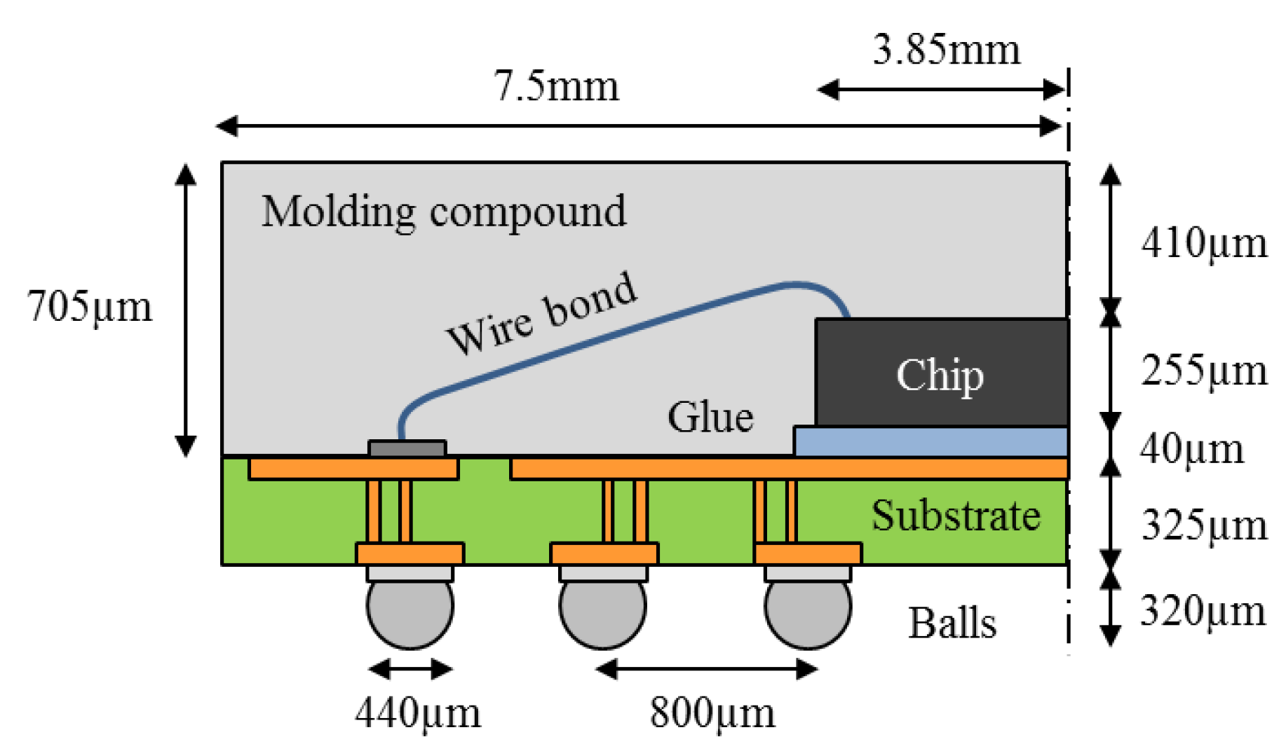
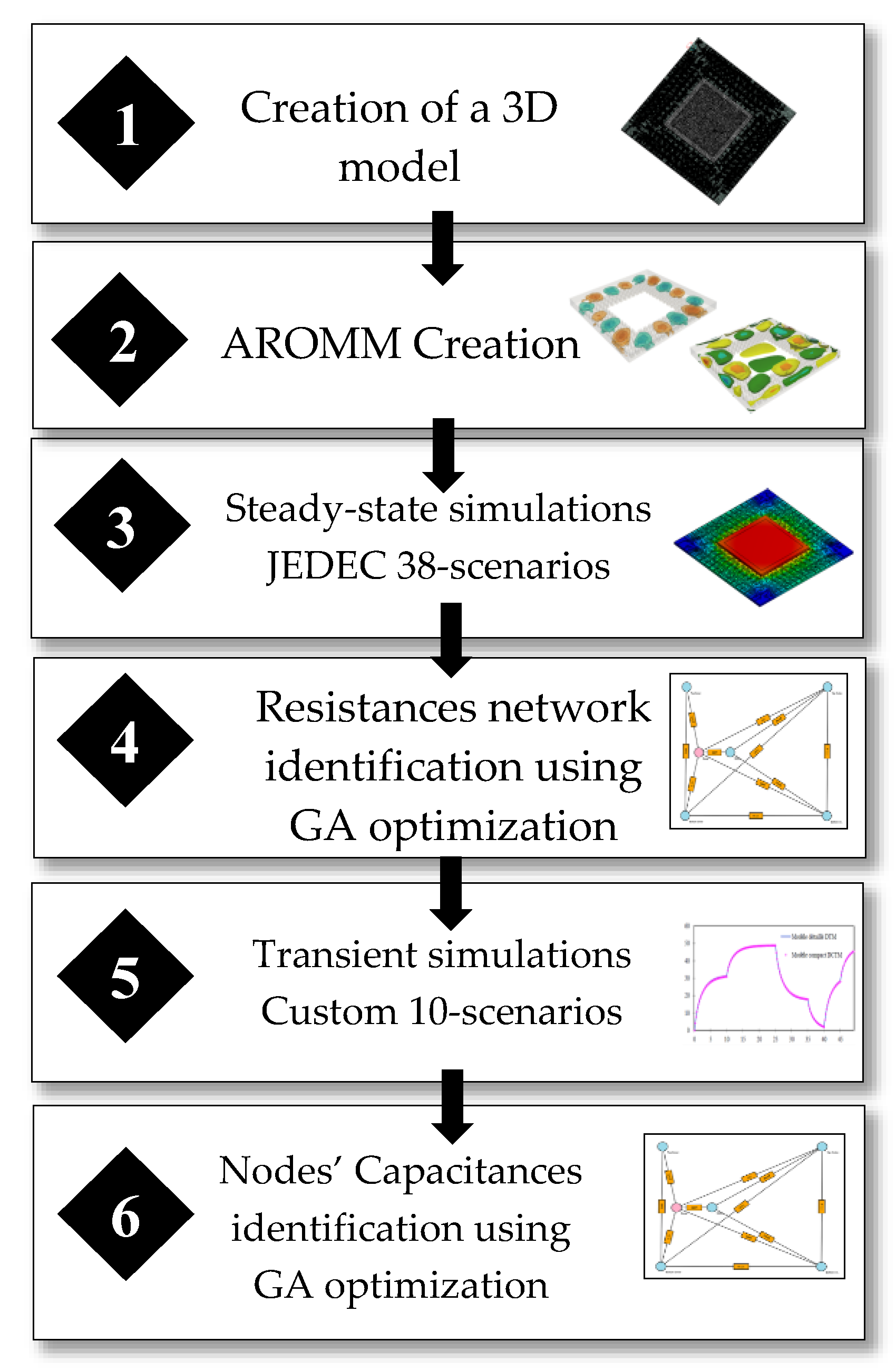
8.4. Steady-State Results

Two cases are presented. They highlight the component thermal behavior when:
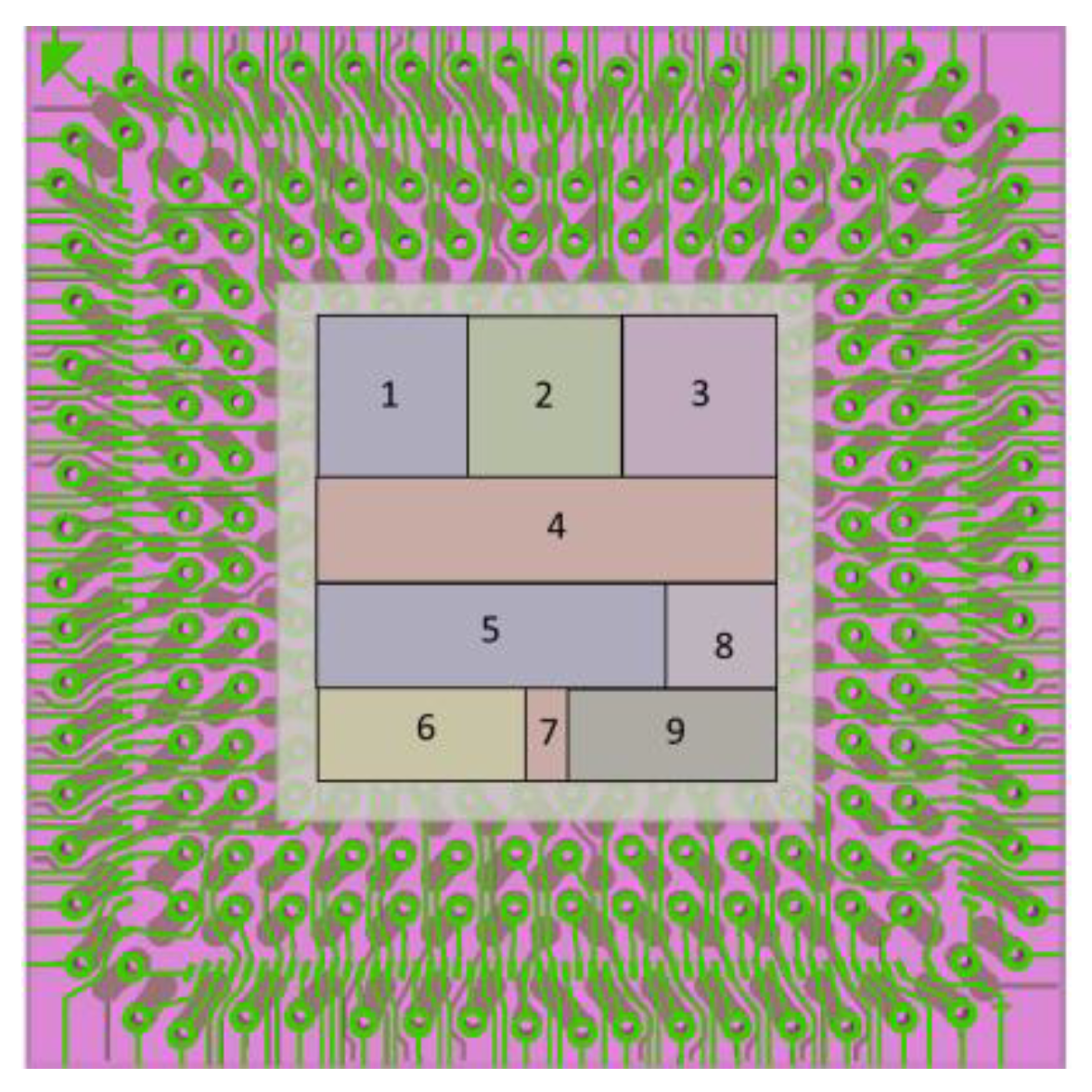
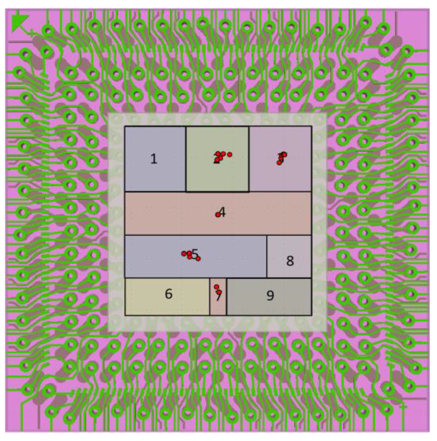
  • Test 1: A power dissipation of 2.6 watts is applied on zone 2
  • Test 2: Zones 3, 5, and 8 are respectively submitted to a power dissipation of 0.41, 0.675, and 0.0975 watts.
The mathematical calculations assume the boundary conditions on package external surfaces presented in Table 6.
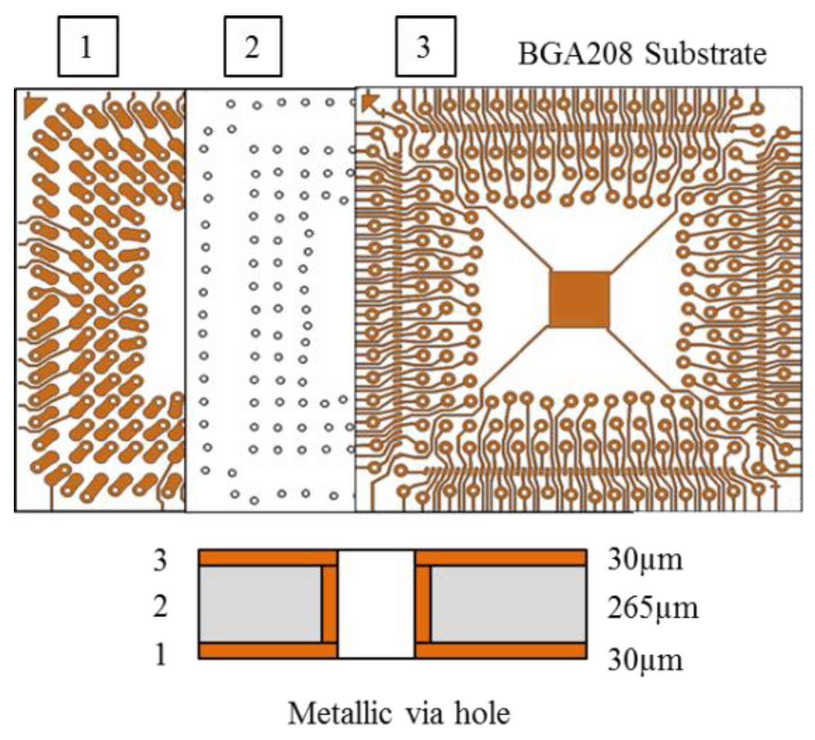
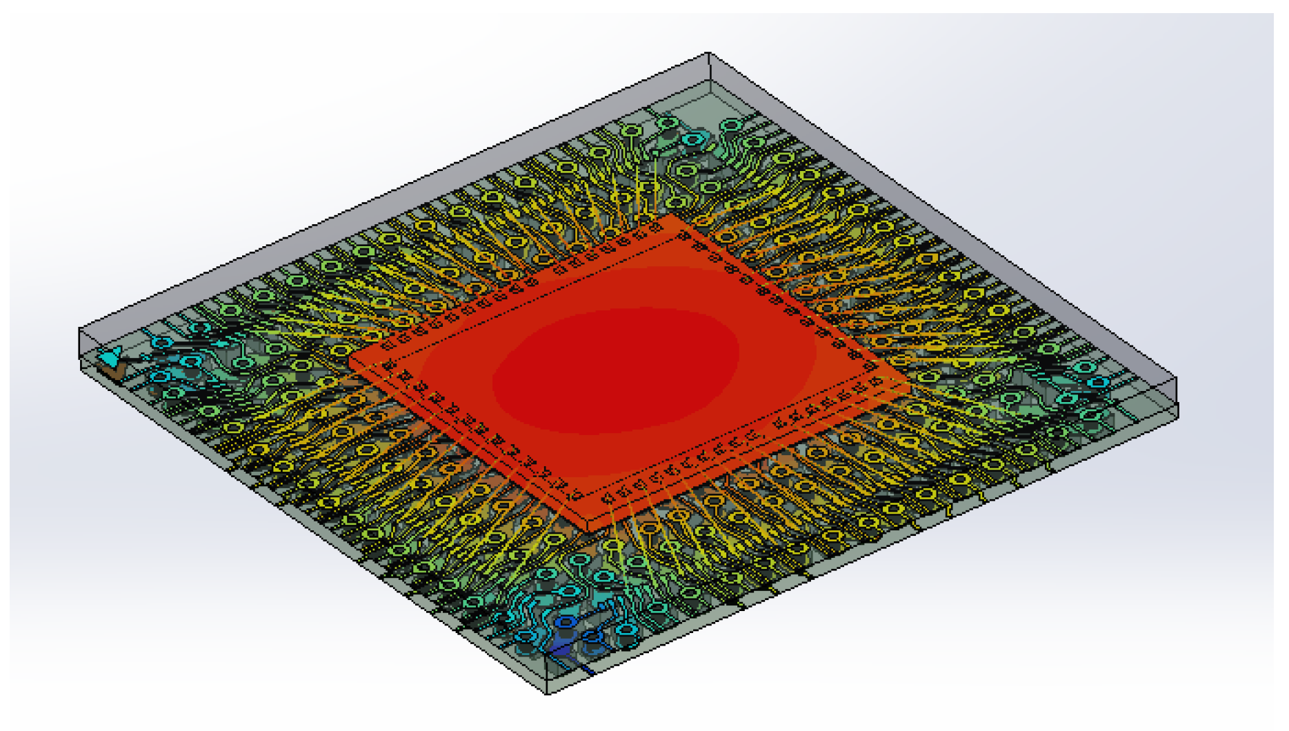
Figure 10 presents the temperature field calculated by the reduced model for the whole package, as well as for the chip on the BGA substrate. The computation time of the derived ROM is lower than 0.5 s for a temporal simulation of 60 s (the time required to reach steady state). The main interest of the modal method lies in its ability to compute, at low cost, the whole temperature field, even for complex geometries such as the BGA packages family. Then, 4.5 s are needed to rebuild the whole temperature field for 101 snapshots. The hot-spot location on the chip, our concern, is properly identified, but fine details are also recovered as the temperature elevation on the copper tracks. The error between the reduced and the finite elements model is also displayed in Figure 10c. In most of the chip, and copper track, the error is below 1 °C (0.8%), which is a very interesting result for this preliminary investigation.
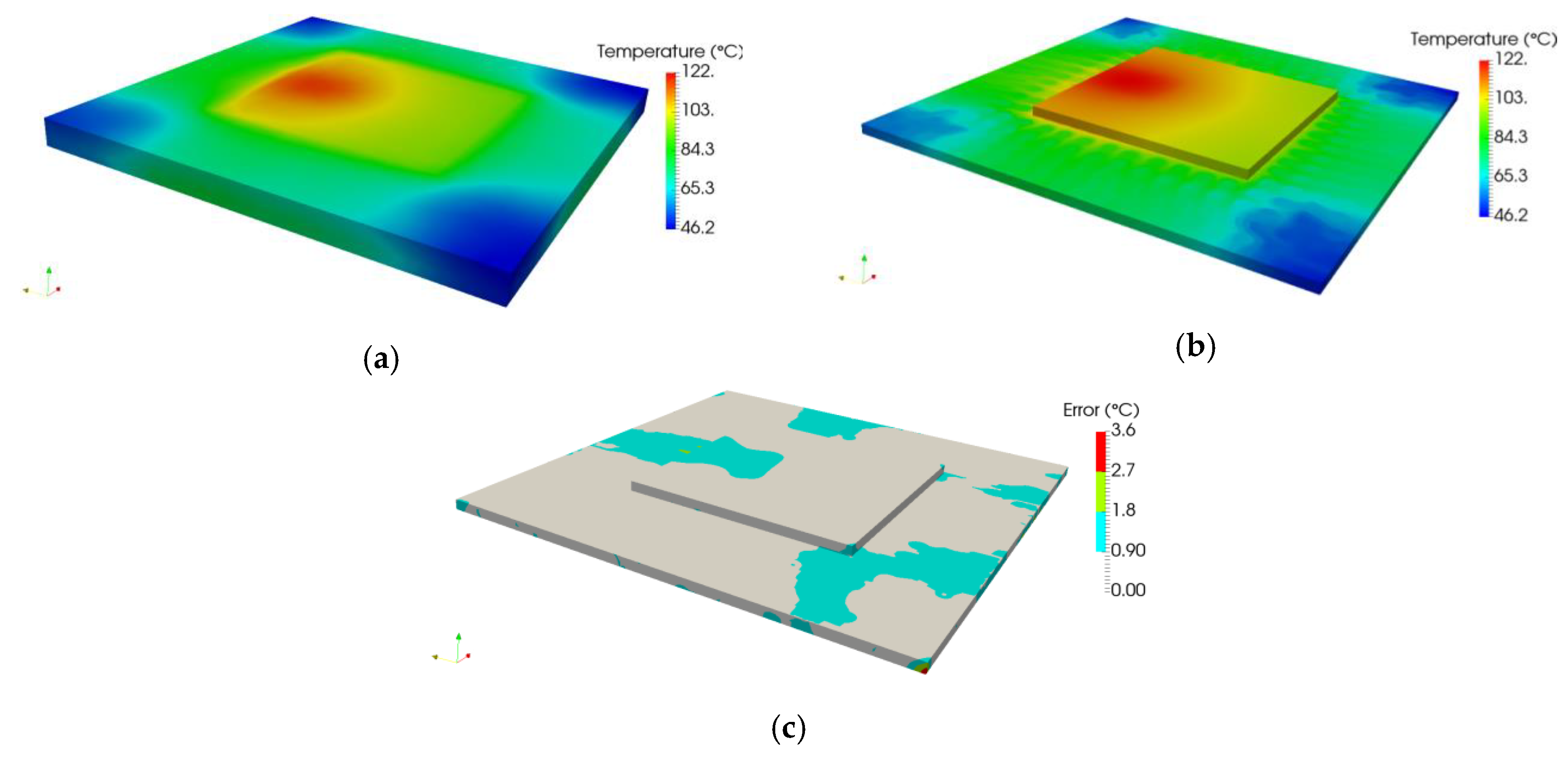
The temperature distribution at steady state for test 2 is presented in Figure 11 As the boundary conditions differ significantly from test 1 and the dissipated power is reduced, the maximum temperature reached by the chip is much lower and is predicted by the modal model with a maximum error of 0.36 °C (1.6%). Obviously, the hot-spot location moves as the different zones are activated, which is well predicted.
Finally, as the temperature field on the chip is different, it substantially affects the heat spreading on the tracks and, thus, the heat distribution on the ball array. The knowledge of the whole temperature field enables the computation of temperature gradients, and opens the way to thermomechanical consideration.

8.5. Transient Results

Dynamic simulations are conducted to compare the thermal prediction of the computed ROM with the FEM simulation (assumed to be the reference) on two test cases. FEM simulations need roughly 47 min to perform a 50 s transient simulation with multi-activations.
Two sets of boundary conditions (different from those presented in Table 6) were chosen and are summarized in Table 7.
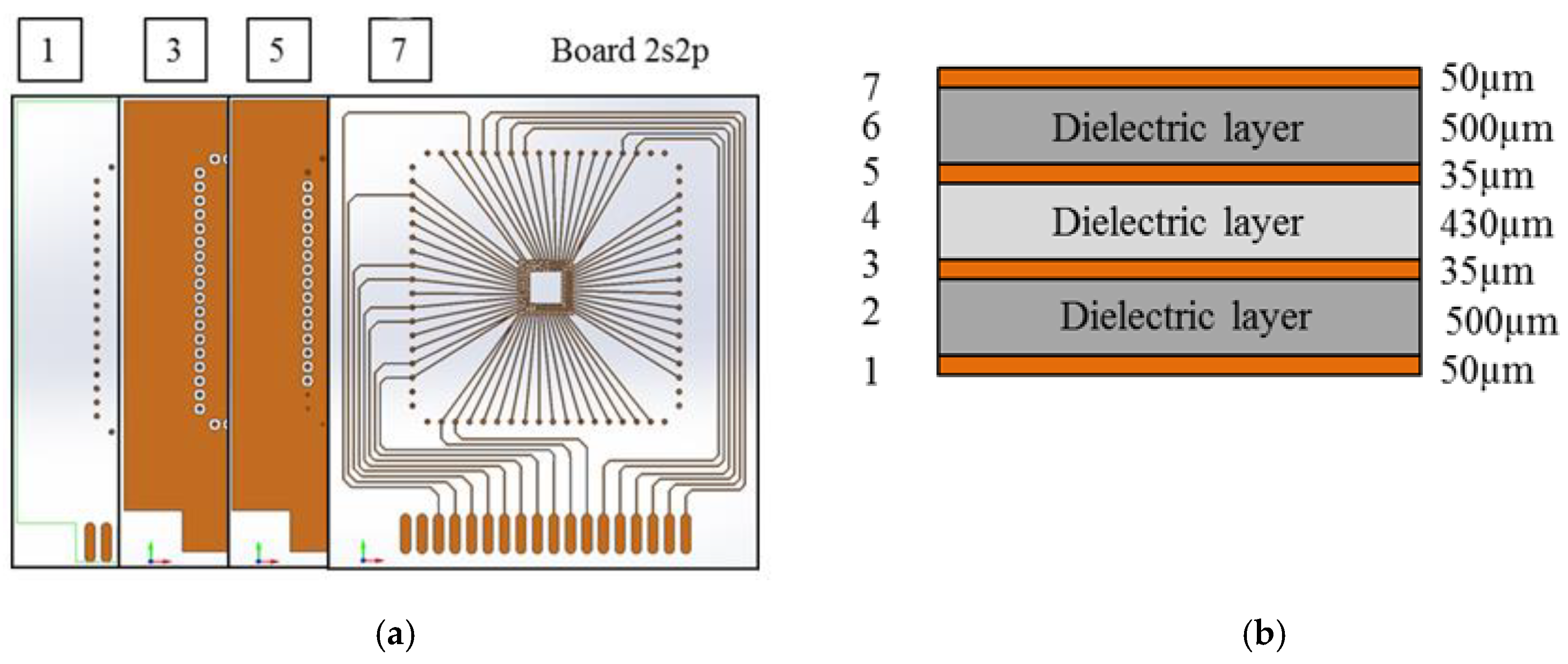
Boundary conditions of Case 1 correspond to a component mounted on a PCB in vertical natural convection plus radiation. Case 2 corresponds to a component sandwiched between the PCB and thermal drain reported on top of the component ( h ¯ T O P integrates all thermal paths: Contact resistances, thermal interface material, and aluminum drain).
Two power transient scenarios are defined: One in which different zones are successively activated, as presented in Table 8, and a second one in which different zones are simultaneously activated, as presented in Table 9. This latter describes a realistic operating case of a BGA. Indeed, power Input-Outputs and firmware are always on and the other functional areas have dynamic activation imposed by software operations.
The computation time required by the reduced model is 4.5 s, which is 600 times faster than that of the finite elements model.
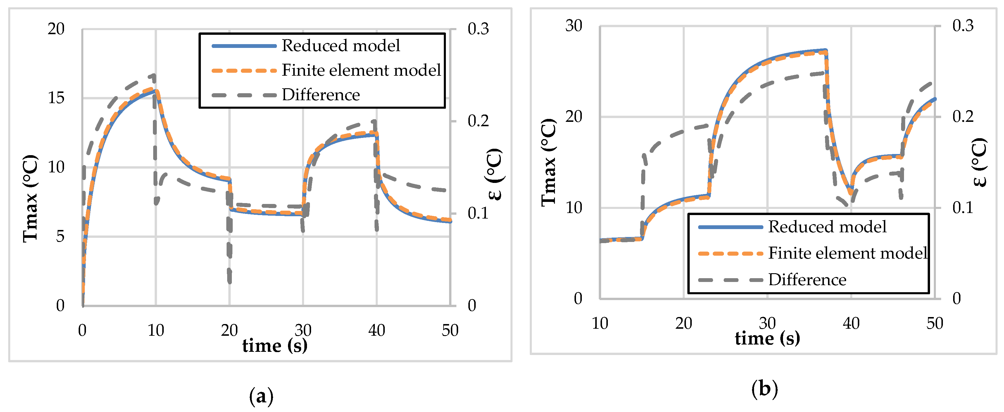
The maximum temperature reached by the chip computed by the amalgamated reduced-order modal model (AROMM) and by the finite elements model has been compared for both cases. Figure 12a,b present the comparison for boundary conditions case 1 with activation profile 1 (Table 8) and boundary conditions case 2 with activation profile 2 (Table 9), respectively.
The agreement on this critical parameter is very good, as it never outreaches 0.25 °C, i.e., a relative difference less than 1.6% for the first case and 1% for the second. A sudden rise in the difference between models is noticed when the power changes. This effect is induced by modal reduction as modes with a high time constant have been discarded.
This very good accuracy on the maximal temperature is accompanied by a satisfying precision on the entire chip. 
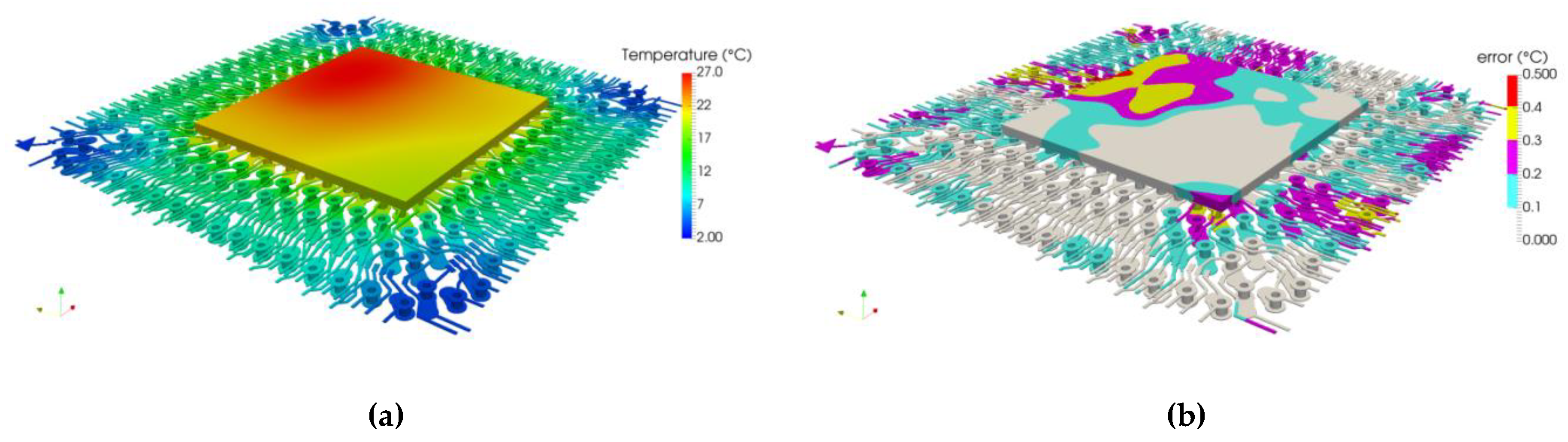
Figure 13 presents the temperature field computed by the reduced model at t = 37 s, i.e., at the time where the error is the most important. The maximal temperature difference on the chip between the reduced model and the FE one is less than 0.5 °C. On most of the chip (and the copper etches), the error is below 0.2 °C, yielding an average error (in time and space) of 0.08 °C.
The error field is erratic, which is characteristic of modal reduction. Thus, the location of the maximum error cannot be known a priori with this method.
Thus, both test cases using different boundary conditions and power profiles confirm the very good accuracy of the ROM, as the error is below 2% for each time step on the chip. Those results validate the new substructuring model order reduction approach to create an AROMM of complex components.
Moreover, as modal methods compute the temperature field in its integrality, there is no need for an a priori definition of the outputs. Indeed, the localizations of the hottest spot of the chip during the transient simulation (depicted by circles) are highlighted in Figure 14.
Obviously, the hot spot moves as the different zones are activated. This simple fact questions the notion of junction temperature. This is confirmed by Figure 15, which compares the maximum temperature reached by the chip to the temperature at the center of the chip: An output at the center of the chip would underestimate the temperature by up to 4 °C, i.e., a relative error of 25%, which is by far greater than the temperature prediction error of the reduced model.
Another main interest of this substructuring modal approach is to have two distinct models, one for the chip and one for all the other parts of the BGA. If one of them is modified, only the latter must be regenerated. In the case of the component, all constituting parts except the die are imposed by the manufacturer, so this model is realized only once. Then, the model of the chip can be easily regenerated to take into account the new spatial power profile or correction of semiconductor thermal properties.
The substructuring modal approach offers a solution to integrate the real spatial power distribution of the component without additional creation and simulation time. Indeed, this power distribution evolves during the development cycle from the uniform power distribution to the real profile based on electric simulation.

9. Conclusions

This study presents a procedure to validate a numerical thermo-fluid model of a complex electronic component, in this case, a ball grid array package of 208 balls. Then, this detailed thermal model is used to derive a dynamic compact thermal model, inspired by the DELPHI methodology, which can be substituted by the DTM to perform a set of thermo-fluidic simulations while preserving the high level of accuracy. To quicken the reduction process, an amalgamated reduced-order modal model is coupled to meta-heuristic optimizations using genetic algorithms. As a main benefit, the overall DCTM creation time is reduced by 86%.
Further, the AROMM method coupled to a substructuring modal method is applied to a BGA208 with, this time, multiple internal heat sources. This novel method allows the building of reduced models independent of boundary conditions (BCI-AROMM). A reduced-order model of only 300 modes was built and will be improved in future works. However, the time needed to create the model remains important, as 8 h of computation were used. Nevertheless, the first deduced model offers very satisfying results as the error on the maximum temperature never outreaches 2%, as well as for steady-state and transient simulations, for a reduction factor of 600 in computation time. Moreover, this model permits us to study, quickly and accurately, all 3-D thermal phenomena involved by the complex structure of the real component. These numerical results should now be confirmed by experimental data, and an experimental setup is being conceived.
Further, a transient characterization is under investigation. The definition of the adjusted heat capacity parameters is based on one-dimensional network identification using stochastic Bayesian deconvolution [23].

Author Contributions

V.B. proposed this approach, performed the numerical models simulations and contributed to the paper redaction. F.J. ran the computations on the substructured model and contributed to the paper redaction. E.M.-V. designed the test vehicle, provided experimental measurements and contributed to the paper redaction. A.N. elaborated the modal substructuration theory. O.D. implemented and optimized the Genetic Algorithms. All authors have read and agreed to the published version of the manuscript.

Funding

This research received no external funding.

Acknowledgments

The authors would like to thank Vincent Fox for his contribution to this work.

Conflicts of Interest

The authors declare no conflict of interest.

Nomenclature

Latin symbols
C volumetric heat capacity [ K / ( m 3 . K ) ]
h heat exchange coefficient [ W / ( m 2 . K ) ]
k thermal conductivity [ W / ( m . K ) ]
R c contact thermal resistance [ m 2 . K / W ) ]
R J A Junction to ambient thermal resistance [K/W]
Q Thermal power [ W ]
T Temperature [°C]
T Air temperature [°C]
x state
V mode [K]
Greek symbols
λ eigenvalue
φ heat flux density [ W / m 2 ]
ϖ volume power [ W / m 3 ]
Superscript
Mmeasurement
Nnumeric
DDirichlet
SSteklov

References

  1. Monier-Vinard, E.; Rogié, B.; Bissuel, V.; Laraqi, N.; Daniel, O.; Kotelon, M.-C. State of the art of numerical thermal characterization of electronic component. In Proceedings of the 17th International Conference on Thermal, Mechanical and Multi-Physics Simulation and Experiments in Microelectronics and Microsystems (EuroSimE), Montpellier, France, 18–20 April 2016. [Google Scholar]
  2. JEDEC Standard JESD15-4. DELPHI Compact Thermal Model Guideline; Jedec Solid-State Technology Association: Arlington, VA, USA, 2008; Available online: https://www.jedec.org/system/files/docs/JESD15-4.pdf (accessed on 8 June 2020).
  3. Atwell, J.A.; King, B.B. Proper orthogonal decomposition for reduced basis feedback controllers for parabolic equations. Math. Comput. Model. 2001, 33, 1–19. [Google Scholar] [CrossRef]
  4. Zhang, X.; Xiang, H. A fast meshless method based on proper orthogonal decomposition for the transient heat conduction problems. Int. J. Heat Mass Transf. 2015, 84, 729–739. [Google Scholar] [CrossRef]
  5. Codecasa, L.; D’Alessandro, V.; Magnani, A.; Rinaldi, N.; Zampardi, P.J. Fast Novel Thermal Analysis Simulation Tool for Integrated Circuits (FANTASTIC). In Proceedings of the 20th International Workshop on Thermal Investigations of ICs and Systems, London, UK, 24–26 September 2014. [Google Scholar]
  6. Joly, F.; Quéméner, O.; Neveu, A. Modal Reduction of an Advection-Diffusion Model Using a Branch Basis. Numer. Heat Transf. Part B Fundam. 2008, 53, 466–485. [Google Scholar] [CrossRef]
  7. Quéméner, O.; Joly, F.; Neveu, A. The generalized amalgam method for modal reduction. Int. J. Heat Mass Transf. 2012, 55, 1197–1207. [Google Scholar] [CrossRef]
  8. Bissuel, V.; Fox, V.; Monier-Vinard, E.; Neveu, A.; Joly, F.; Daniel, O. Multi-port Dynamic Compact Thermal Models of BGA package using Model Order Reduction and Metaheuristic Optimization. In Proceedings of the 2019 18th IEEE Intersociety Conference on Thermal and Thermomechanical Phenomena in Electronic Systems (ITherm), Las Vegas, NV, USA, 28–31 May 2019. [Google Scholar]
  9. Rogié, B.; Codecasa, L.; Monier-Vinard, E.; Bissuel, V.; Laraqi, N.; Daniel, O.; D’Amore, D.; Magnani, A.; d’Alessandro, V.; Rinaldi, N. Multi-port dynamic compact thermal models of dual-chip package using model order reduction and metaheuristic optimization. Microelectron. Reliab. 2018, 87, 222–231. [Google Scholar] [CrossRef]
  10. Grosjean, S.; Joly, F.; Vera, K.; Neveu, A.; Monier-Vinard, E. Reduction of an electronic card thermal problem by the modal substructuring method. In Proceedings of the IHTC-16, Beijing, China, 10–15 August 2018. [Google Scholar]
  11. Grosjean, S.; Gaume, B.; Joly, F.; Vera, K.; Neveu, A. A modal substructuring method for non-conformal mesh. Application to an electronic board. Int. J. Therm. Sci. 2020, 152, 106298. [Google Scholar] [CrossRef]
  12. Codecasa, L.; Bornoff, R.; Dyson, J.; d’Alessandro, V.; Magnani, A.; Rinaldi, N. Versatile MOR-based boundary condition independent compact thermal models with multiple heat sources. Microelectron. Reliab. 2018, 87, 194–205. [Google Scholar] [CrossRef]
  13. Rogié, B.; Grosjean, S.; Monier-Vinard, E.; Bissuel, V.; Joly, F.; Daniel, O.; Laraqi, N.; Vera, K. Delphi-like dynamical compact thermal models using model order reduction based on modal approach. In Proceedings of the 34th Thermal Measurement, Modeling & Management Symposium (SEMI-THERM), San Jose, CA, USA, 19–23 March 2018. [Google Scholar]
  14. JEDEC Standard JESD51. Methodology for the Thermal Measurement of Component Packages; Jedec Solid-State Technology Association: Arlington, VA, USA, 2008; Available online: https://www.jedec.org/system/files/docs/Jesd51.pdf (accessed on 8 June 2020).
  15. JEDEC Standard N°51-3. Low Effective Thermal Conductivity Test Board for Leaded Surface Mount Packages; Jedec Solid-State Technology Association: Arlington, VA, USA, 1996; Available online: https://www.jedec.org/system/files/docs/JESD51-3.PDF (accessed on 8 June 2020).
  16. JEDEC Standard N°51-7. High Effective Thermal Conductivity Test Board for Leaded Surface Mount Packages; JEDEC Solid-State Technology Association: Arlington, VA, USA, 1999; Available online: https://www.jedec.org/system/files/docs/jesd51-7.PDF (accessed on 8 June 2020).
  17. JEDEC Standard N°51-2a. Integrated Circuit Thermal Test Method Environmental Conditions—Natural Convection (Still Air); Jedec Solid-State Technology Association: Arlington, VA, USA, 2002; Available online: https://www.jedec.org/system/files/docs/JESD51-2A.pdf (accessed on 8 June 2020).
  18. JEDEC Standard N°51-6. Integrated Circuit Thermal Test Method Environmental Conditions—Forced Convection (Moving Air); Jedec Solid-State Technology Association: Arlington, VA, USA, 1999; Available online: https://www.jedec.org/system/files/docs/jesd51-6.pdf (accessed on 8 June 2020).
  19. Monier-Vinard, E.; Rogié, B.; Bissuel, V.; Laraqi, N.; Daniel, O.; Kotelon, M.-C. State of the Art of Thermal Characterization of Electronic Components using Computational Fluid Dynamic tools. Int. J. Numer. Methods Heat Fluid Flow 2017, 27. [Google Scholar] [CrossRef]
  20. Laffay, P.O.; Quéméner, O.; Neveu, A.; Elhajjar, B. The Modal Substructuring Method: An Efficient Technique for Large-Size Numerical Simulations. Num. Heat Transf. Part B Fundam. 2011, 60, 278–304. [Google Scholar] [CrossRef]
  21. Monier-Vinard, E.; Bissuel, V.; Rogié, B.; Laraqi, N.; Daniel, O.; Kotelon, M.-C. Evolution of the DELPHI Compact Thermal Modelling Method: An Investigation on the Boundary Conditions Scenarios. In Proceedings of the THERMINIC XXII, Budapest, Hungary, 21–23 September 2016. [Google Scholar] [CrossRef]
  22. Monier-Vinard, E.; Dia, C.; Bissuel, V.; Laraqi, N.; Daniel, O. Latest developments of Compact Thermal Modeling of System in Package devices by means of Genetic Algorithm. In Proceedings of the ITHERM XIV, Orlando, FL, USA, 27–30 May 2014. [Google Scholar] [CrossRef]
  23. Lai, W.; Liu, X.; Chen, W.; Lei, X.; Tang, X.; Zang, Z. Transient multi-exponential signals analysis using Bayesian deconvolution. Appl. Math. Comput. 2015, 265, 486–493. [Google Scholar]
Figure 1. Semi-cross-section of the studied BGA208.
Energies 13 02968 g001
Figure 2. BGA208’s laminate description.
Energies 13 02968 g002
Figure 3. JEDEC 2s2p thermal test boards: Copper traces definition (a) and stack-up (b).
Energies 13 02968 g003
Figure 4. Standardized experimental setups for natural convection (a) and forced convection (b).
Energies 13 02968 g004
Figure 5. Sub-decomposition of the domain.
Energies 13 02968 g005
Figure 6. BGA208’s numerical model.
Energies 13 02968 g006
Figure 7. Hybrid dynamic compact thermal model (DCTM) creation flow.
Energies 13 02968 g007
Figure 8. Chip partitioning in nine zones.
Energies 13 02968 g008
Figure 9. Sensitive temperatures encountered by the chip with uniform power dissipation (a) and localized on a peculiar area (b).
Energies 13 02968 g009
Figure 10. Temperature field with molded resin (a), without (b), and error field (c) at steady state for Test 1.
Energies 13 02968 g010
Figure 11. Temperature field for three active heat sources.
Energies 13 02968 g011
Figure 12. Temporal evolution of the maximum temperature reached by the ball-grid-array (BGA)–difference on this parameter between the reduced and the finite element model for test case 1 (a) and 2 (b).
Energies 13 02968 g012
Figure 13. Temperature field (a) computed by the reduced model of order 300 at t = 37 s. Error (b) with the finite elements simulation at the same time.
Energies 13 02968 g013
Figure 14. Localization of the maximal temperature reached by the chip during the transient simulation.
Energies 13 02968 g014
Figure 15. Temporal evolution of the maximum temperature reached by the BGA and the temperature at the center of the chip—Difference between those two quantities.
Energies 13 02968 g015
Table 1. Reference material properties.
ConstituentMaterialk (W/(m.K))
Molding CompoundResin0.66
Wire bondGold320
ChipSilicon148
Chip attach adhesiveSilver Glue2.1
Signal layer and viaCopper400
Dielectric layerFR40.38
Solder ball63Sn37pb51
Table 2. Experimental RJA measurement of BGA208 mounted on the 2s2p board.
Convection Mode T (°C) Q (W) U (m/s) R J A M (K/W)
Natural22.52.001029.21
Forced21.13.037125.37
20.73.02223.91
20.73.06322.87
Table 3. Reference properties for both JEDEC boards.
ConstituentMaterialk (W/(m.K))
Signal layer and viaCopper400
Dielectric layerFR40.38
Table 4. Fitting of the 2s2p thermal metrics (Icepak®).
T (°C) Q (W) U (m/s) R J A M (K/W) R J A N (K/W)%E
22.52.001029.2129.33<1%
21.13.037125.3725.45<1%
20.73.02223.9124.11<1%
20.73.06322.8723.07<1%
Table 5. Approximation of 2s2p thermal metrics (Icepak®).
T (°C) Q (W) V (m/s) R J A M (K/W) R J A D C T M (K/W)%E
22.52.001029.2129.731.8%
21.13.037125.3725.091.1%
20.73.02223.9123.511.7%
20.73.06322.8722.163.1%
Table 6. Heat transfer coefficients definition (W/(m2.K)).
C a s e h ¯ T O P h ¯ B O T T O M h ¯ S I D E S
Test 15025015
Test 2100040100
Table 7. Heat transfer coefficients definition (W/(m2.K)).
C a s e h ¯ T O P h ¯ B O T T O M h ¯ S I D E S
Test 12080010
Test 220050020
Table 8. Activation of the different zones of the chip for transient simulation number 1.
Active Zone φ (W/m3) Q (W)Time (s)
Zone 4 8.2 · 10 9 0.8130–10
Zone 7 8.0 · 10 9 0.16210–20
Zone 5 2.2 · 10 9 0.16420–30
Zone 3 9.6 · 10 9 0.49730–40
Zone 2 2.0 · 10 9 0.10340–50
Table 9. Activation of the different zones of the chip for transient simulation number 2.
Active Zone φ (W/m3) Q (W)Time (s)
Zone 1 4.45 · 10 9 0.2315–23
Zone 2 9.09 · 10 9 0.4723–37 and 46–50
Zone 3 9.09 · 10 9 0.4723–37
Zone 4 1.11 · 10 9 0.110–50
Zone 5 3.47 · 10 9 0.2640–46
Zone 6---
Zone 7 4.44 · 10 9 0.3640–50
Zone 8---
Zone 9 3.46 · 10 9 0.140–50

