Article

Reliability Characterization of Gallium Nitride MIS-HEMT Based Cascode Devices for Power Electronic Applications

1
Department of Mechanical Engineering, National Chiao Tung University, Hsinchu City 30010, Taiwan
2
Department of Material Science and Engineering, National Chiao Tung University, Hsinchu City 30010, Taiwan
*
Author to whom correspondence should be addressed.
These authors contributed equally to this work.
Energies 2020, 13(10), 2628; https://doi.org/10.3390/en13102628
Submission received: 17 April 2020 / Revised: 15 May 2020 / Accepted: 18 May 2020 / Published: 21 May 2020
(This article belongs to the Special Issue Reliability of Power Electronic Systems)

Abstract

:
We present a detailed study of dynamic switching instability and static reliability of a Gallium Nitride (GaN) Metal-Insulator-Semiconductor High-Electron-Mobility-Transistor (MIS-HEMT) based cascode switch under off-state (negative bias) Gate bias stress (VGS, OFF). We have investigated drain channel current (IDS, Max) collapse/degradation and turn-on and rise-time (tR) delay, on-state resistance (RDS-ON) and maximum transconductance (Gm, max) degradation and threshold voltage (VTH) shift for pulsed and prolonged off-state gate bias stress VGS, OFF. We have found that as stress voltage magnitude and stress duration increases, similarly IDS, Max and RDS-ON degradation, VTH shift and turn-on/rise time (tR) delay, and Gm, max degradation increases. In a pulsed off-state VGS, OFF stress experiment, the device instabilities and degradation with electron trapping effects are studied through two regimes of stress voltages. Under low stress, VTH shift, IDS collapse, RDS-ON degradation has very minimal changes, which is a result of a recoverable surface state trapping effect. For high-stress voltages, there is an increased and permanent VTH shift and high IDS, Max and RDS-ON degradation in pulsed VGS, Stress and increased rise-time and turn-on delay. In addition to this, a positive VTH shift and Gm, max degradation were observed in prolonged stress experiments for selected high-stress voltages, which is consistent with interface state generation. These findings provide a path to understand the failure mechanisms under room temperature and also to accelerate the developments of emerging GaN cascode technologies.

Graphical Abstract

1. Introduction

Gallium Nitride (GaN) power devices play a vital role in power conversion applications [1,2,3], achieving extraordinary capabilities in photonics and semiconductor technology. In recent decades, GaN high-electron-mobility-transistors (HEMTs) have shown high performance under high temperature (up to 200 °C) [4,5], high breakdown voltage (>650 V) [2,3] and high frequency (>1 MHz) [6,7] operating conditions. Based on these qualities, GaN-HEMT becomes an alternative and competitive candidate to silicon for future semiconductor technology [8]. In the case of switching applications, the gate channel of GaN HEMT with a metal-insulator-semiconductor (MIS-HEMT) structure, which shown in Figure 1a, provides an enlarged gate swing. Due to the addition of a gate insulator, it becomes very effective towards suppressing the gate leakage current (IGS, Off), thus improving long-term reliability compared to its conventional equivalent [9,10]. From these advantages, GaN HEMTs with MIS structure are used in a wide range of applications like electric vehicles, hybrid electric vehicles, and photovoltaic devices [11,12,13].
Normally in switching applications, enhancement mode (E-mode) switches need highly accurate control to get narrow gate swing regarding spikes [14,15] while commonly available gate drivers are very difficult to provide the required negative drive voltage on depletion mode (D-mode) devices [16,17]. To avoid the deficiencies of the above approaches in GaN power switches, cascode power switch configurations were developed, which combines high voltage (HV) D-mode GaN MIS-HEMT connected in series with a low voltage (LV) Si-MOSFET device [18,19], as shown in Figure 1b. GaN cascode configuration achieved a high quality in terms of high breakdown voltage (1200 V), high thermal performance and extended gate drive safety margin (10 V). On the other hand, it also achieved higher reliability qualities, such as maximum transient protection (800 V) and extended JEDEC, AEC-Q101 qualifications, than the commercialized E-mode GaN. In this hybrid cascode configuration, D-mode devices can act like E-mode devices, thus achieving maximum acceptability and applicability. The on-state and off-state of the HV D-mode GaN MIS-HEMT device are controlled using LV Si-MOSFET, which makes the cascode power switch compatible with Si gate-drivers and provides a sufficient safety driving margin for the HV D-mode GaN switch. The body diode in the cascode configuration plays a role in reduced power consumption and support for peripheral components. This cascode configuration offers an extended operating voltage for HV GaN HEMT power systems. However, the GaN power switches dynamic switching problems and static reliability problems still present limitations to the market penetration for advanced GaN in semiconductor technology.
Gate lag (Pulsed Off-State Gate Bias Stress) is the phenomenon in which the drain current shows slow transients for abrupt change in gate voltage and causes a serious problem for analog and digital III-V field effect transistors as results [20,21]. The device’s main parameters, such as IDS, RDS-ON, VTH, and RF power variation and degradation, are observed with respect to the short duty cycle of off-state VGS bias stress. Several gate-lag effects have been reported in GaN based FET and correlated to current-collapse problems reducing RF power performance of the devices [22,23,24]. These gate-lag effects are caused by surface state generation at the ungated region of the device and held responsible for observed phenomena. During the off-state pulsed VGS bias stress, the leaking electrons from the gate metal are trapped or detrapped by the surface states and are concerned as far as the mechanism behind surface states charging or discharging. These traps act like “virtual gates”, which are responsible for carrier capture and capture emission phenomena from traps with time leading towards delay of rise-time (tR) and degradation of drain current during switching conditions [25,26]. Off-state gate pulse-induced surface states trap the region modulated in the density of negatively charged traps with an increase in the magnitude of gate bias stress and evolution of stress time.
Negative bias instability has been found as a critical reliability issue in power transistors, such as MOSFETs, which are made of many material systems, such as Si, SiC, and particularly with GaN. Under reverse gate bias stress, positive charge can be trapped at interface-states in near-interface defects, which are border traps [27]. These trapped charges play a role on the negative threshold voltage (VTH) shift and also degrade channel carrier mobility [28,29]. A similar observation was reported in SiC MOSFETs, where a partially recoverable decrease in lifetime and increase in interface state density took place after reverse gate bias stress [30]. Based on previous studies on GaN power devices, under negative gate bias stress, the GaN HEMT and MIS-HEMT showed a significant negative VTH shift, which is a typical behavior with other material systems, and for enhancement-mode GaN MOSFETs, a positive VTH shift was observed [31]. These observations suggests that the electron trapping in the GaN region results in a positive VTH shift. Moreover, compared to other GaN power devices, the recent understanding of prolonged off-state gate bias stress effects on the GaN based cascode power switch is very limited. This is mainly due to the configuration structure and multi-layered gate stack with multiple interfaces, which presents more chances for its electron tapping effects. A wider study is needed to provide a solid understanding of the mechanism behind negative gate bias stress in GaN cascode technology.
This paper contributes an understanding of the surface and oxide related trapping processes in GaN cascode power switches during off-state VGS bias stress. The results of trapping processes described below indicate that: (i) in pulsed off-state bias the surface trapping may constitute a relevant parasitic mechanism that continuously limits dynamic performance of the switch; (ii) in prolonged off-state gate stress bias, the oxide-related trapping and interface state generation may constitute a relevant threshold voltage (VTH) shift, transconductance (Gm, max) degradation, and rise-time (tR) delay increase, with increasing stress voltage magnitude and stress time evolution at room temperature. The major issue in the presence of electronic traps in the GaN power switch structure limits performance continuously.

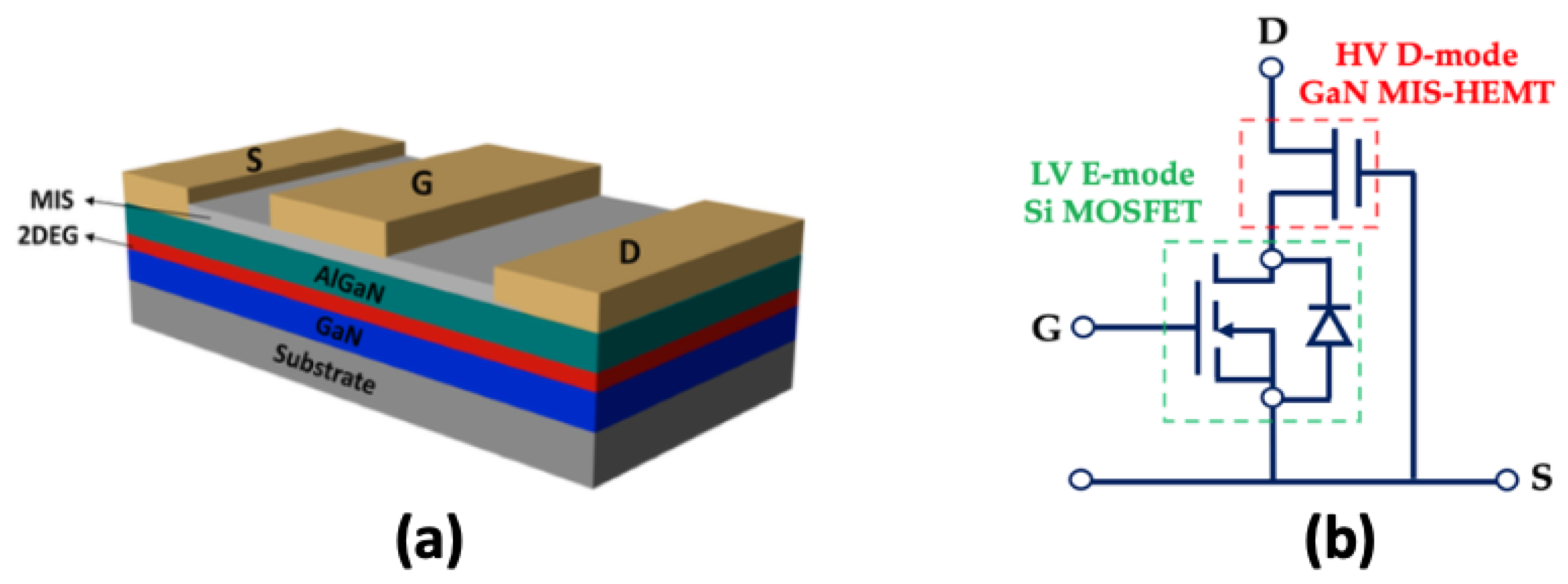
2. Experimental Details

This paper contains the study of dynamic instability and static reliability that has been carried out on a commercialized 650 V breakdown voltage and 130 mΩ maximum on-state resistance GaN MIS-HEMT-based cascode power switch from a manufacturer. Initially have investigated the electrical characteristics, such as IDS-VDS and IDS-VGS of a virgin GaN cascode power switch before pulsed and prolonged off-state gate bias stress measurements, which are shown in Figure 2. From virgin IDS-VGS characteristics, main device parameters of threshold voltage VTH = 2.6 V (defined at IDS = 1 A/mm), on-state resistance (RDS-ON) (defined at maximum drain saturation current IDS, Max at VDS = 5 V), and maximum transconductance (Gm, max) were confirmed with the data sheet before off-state gate bias experiments. Further GaN cascode switches were subjected to an extensive trapping-effect analysis based on pulsed and prolonged off-state VGS, OFF bias at room temperature. All these experiments were carried out in a Keithley 2651A and 2601A Source meter system at room temperature.
In the pulsed off-state gate bias stress (Gate-Lag), we characterized the impact of negative gate bias (VGS, OFF) pulsed stress on device behavior through the device parameter stability. A double pulse technique was used in the pulsed off-state stress experiment [32,33,34,35]. The device’s main parameters, threshold voltage (VTH) instability, maximum drain channel current (IDS, Max) collapse, and on-state resistance (RDS-ON) degradation were studied during pulsed VGS, OFF stress through two regimes. The impact of low/mid VGS, OFF pulse stress on the performance of the GaN cascode were observed in the first regime, where the device pulsed with VGS,OFF = −5 to −20 V and VDS = 0 to 5 V at room temperature. Similarly, in the second regime, the device with high-stress voltages of VGS, OFF pulse = −25 to −40 V. During VGS, OFF pulsed stress, the dynamic instabilities with an electron trapping effect on the device were monitored through IDS, Max collapse and RDS-ON degradation, VTH shift and turn-on or rise-time (tR) delay. At each pulse of VGS, OFF stress, the GaN cascode device was stressed for 300 μs and the on-state pulse was 300 ms. Figure 3 shows the flow chart and stress waveform schematic of the pulsed off-state gate (VGS, OFF) stress bias experiment.
In the prolonged gate stress bias experiment, we characterized the negative bias instability on the GaN cascode device at room temperature through the device parameters instability at the linear operating region (VDS = 5 V). More specifically, we studied the stability of the threshold voltage (VTH), which is defined at IDS = 1 A and maximum transconductance (Gm, max). The prolonged VGS, OFF stress phases include a series of stress segments of increasing VGS, OFF and time evolution of stress tstress. When the device is subjected into VGS, OFF stress, both source and drain channels are grounded with VDS = 0 V. Based on the pulsed off-state gate stress bias results, the GaN cascode device is subjected to prolonged off-state gate bias stress experiments with selected high-stress voltages of VGS, OFF = −30 to −40 V. For each VGS, OFF bias stress experiment, different GaN cascode devices are used in this study. In this experiment also, the device is initially subjected to virgin IDS-VGS characterization with VDS = 5 V before VGS, OFF stress. Further, the device has been subjected to high-stress voltages for 5000 s, and during the stress experiment, IDS-VGS characteristics are observed every 1000 s interval. The device threshold voltage (VTH) shift and transconductance (Gm, max) degradation were observed during the stress phase and after the stress experiment. The prolonged off-state gate bias experimental flow chart is shown in Figure 4.

3. Results and Discussion

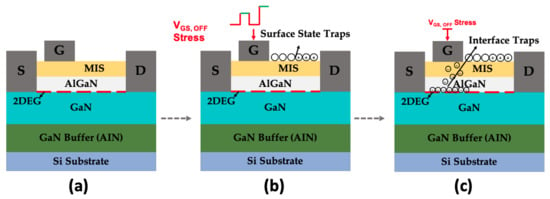
3.1. Pulsed Negative Gate Bias Stress (Gate Lag)

Our study shows behaviors on two regimes of IDS, Max degradation, turn-on delay (tR), negative VTH shift, and RDS-ON degradation for the GaN cascode under pulsed off-state gate stress bias experiment. We have applied a pulsed negative VGS, OFF starting from two different quiescent bias points: VGS, OFF bias = 0 V and VDS = 5 V, which are virgin characteristics and VGS, OFF bias = −5, −10, −15, up to, −40 V with VDS = 5 V, which can induce measurable trapping processes on the GaN cascode switch. In the first regime, under low/mid VGS, OFF pulsed bias stress, the device has minimal IDS, Max collapse, a negligible turn-on delay to reach the max drain output, recoverable ΔVTH shift, and ΔRDS-ON, which is shown in Figure 5. The ΔVTH and ΔRDS-ON are normalized VTH and RDS-ON, which are defined with fresh and stressed values (RDS-ON stress/RDS-ON fresh). In the second regime, the device exposing results of increased IDS, Max degradation, permanent negative ΔVTH shift, high ΔRDS-ON degradation, and increased turn-on delay of device under high VGS, OFF stress is shown in Figure 6.
In this pulsed VGS, OFF bias stress experiment, as the evolution stress pulse width and magnitude of stress voltage increases, the VTH instability and RDS-ON degradation of the device also continuously increases for relevant trapping effects on the device. Figure 5a shows the device IDS-VGS characteristics over low/mid VGS, OFF pulsed stress voltages at low temperature (room temperature). From Figure 5a during low/mid VGS, OFF pulsed stress, the ΔVTH shift and ΔRDS-ON degradation of the device were extracted, which is shown in Figure 5b. The negative ΔVTH shift for low/mid VGS, OFF stress is very minimal and negligible. Under low-stress, a recoverable IDS, Max collapse and ΔRDS-ON degradation is observed, which is shown in Figure 5a,b. As the VGS, OFF pulsed stress increases to −20 V, IDS, max degradation increases along with turn-on delay to reach the drain saturation current, which indicates the generation of surface traps at the ungated access region [36]. As VGS, OFF stress has a higher increase at room temperature, the IDS, Max degradation further increases, which is shown in Figure 6a. The strong reduction in the drain saturation current IDS, Max is observed due to the generation of surface state traps. The IDS, Max defined at VDS = 5 V and VGS = 10 V changes from 44.5 to 30.5 A, and this is attributed to the reduction of the conduction channel, which is caused by the generation surface straps under VGS, OFF pulsed stress. Eventually, ΔRDS-ON degradation also increases along with IDS, Max degradation for high VGS, OFF pulsed stress. On the other hand, as we increase the VGS, OFF pulsed stress voltages, the negative ΔVTH shift also increases. Figure 6b is an example of this transition with VGS, OFF pulses (−25, −30, −35, and −40 V). This high increase in a negative ΔVTH shift is consistent with electron detrapping from preexisting oxide traps [36,37].
Figure 7a shows the IDS versus time (t) measured from the GaN cascode device in response to the VGS, OFF pulses featuring various VGS, OFF values. Gate lag is asymmetrical, it delays the turn-on transient, leaving the turn-off one almost unaffected. Moreover, the gate lag effects of turn-on delay to reach the maximum drain saturation current are significant in the GaN cascode device. The delay in reaching the IDS, Max of the device has no changes for low/mid stress voltages. As the VGS, OFF pulse value increases, the turn-on delay also increases, which is shown in Figure 7a. The maximum gate lag effect is observed at VGS, OFF = −40 V and is shown in Figure 7a. These gate-lag effects, shown in Figure 7a, by the GaN cascode device originated by the generation of surface traps at the ungated access region. From this observation, the gate-lag transient composed by a fast change in drain current IDS takes place immediately after the application of the VGS turn-on step, followed by a delayed increase of IDS. Both fast and slow components depend on VGS, OFF and VDS values. Figure 7b shows a negative VTH shift and also the rise-time tR delay for the GaN cascode device after the VGS, OFF experiment with VGS, OFF pulse stress = −40 V and VDS = 5 V. By increasing VDS for VGS, OFF pulse, gate lag effects are strongly attenuated with increasing magnitude of turn-on delay and rise-time delay.
These observations suggest that the generation of field-induced surface traps at the ungated access region between gate and drain sides and electron detrapping effects from preexisting oxide traps induces the IDS, Max and ΔRDS-ON degradation [38,39,40], turn-on and rise-time delay, and negative ΔVTH shift [29,30], which is shown in Figure 5, Figure 6 and Figure 7. The generation of ungated surface-state traps between the gate and source/drain contacts act as “virtual gates”, modulating the underlying depletion region through changes in the density of negatively charged traps. When the off-state gate bias is changed abruptly, these virtual gates respond with the time characteristics of carrier capture/emission phenomena, thus leading to IDS and ΔRDS-ON degradation and delayed switching performance. The charging/discharging from surface-state traps with off-state gate pulsed bias stress is concerned as the mechanism behind the device performance degradation. Under off-state gate VGS, OFF pulsed bias stress, the electron detrapping effects from the preexisting oxide traps play a role on the negative VTH shift. Figure 9 shows that the schematic diagram of the device illustrates possible surface state electron trapping between the drain and gate channel at the ungated region and electron detrapping effects from oxide traps/trapping under the gate channel.

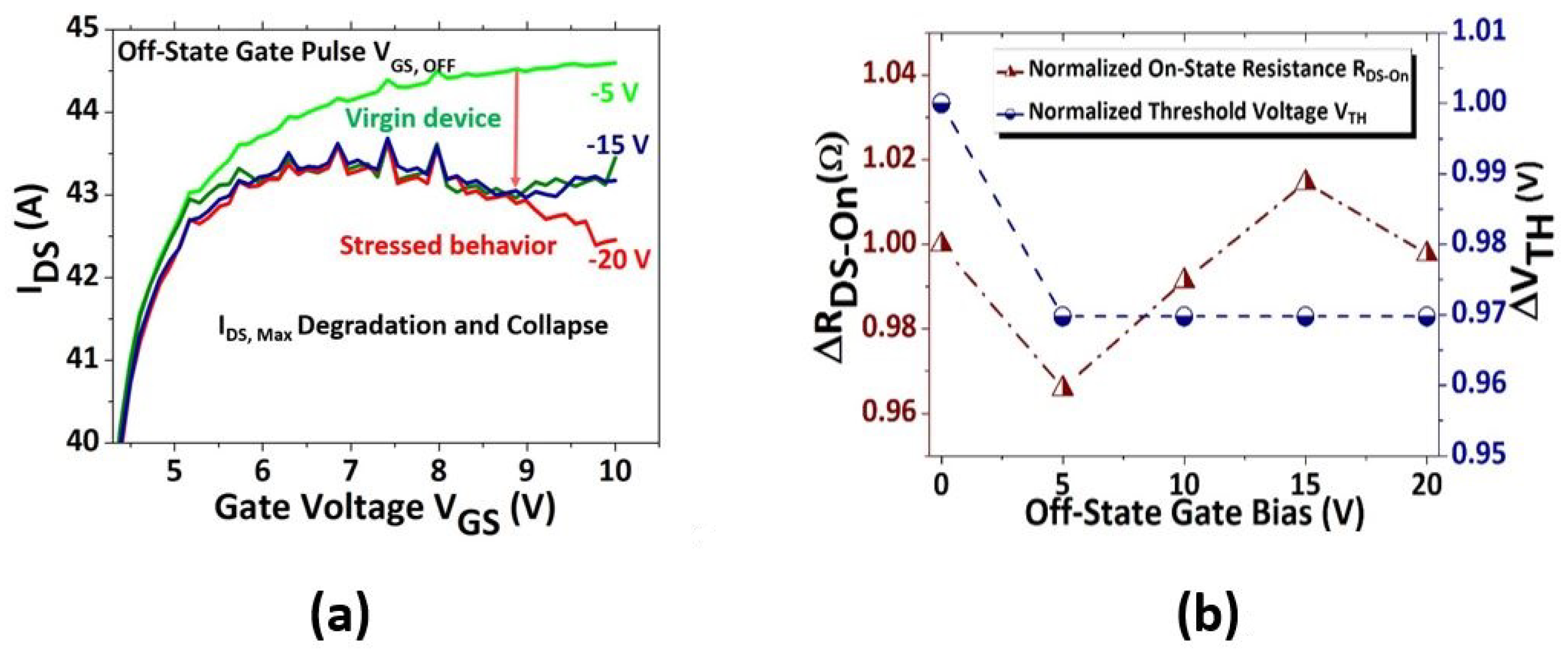
3.2. Prolonged Off-State Gate Bias Stress

Our study focused on selected high VGS, OFF stress voltages based on pulsed (VGS, OFF) stress results. In prolonged off-state gate VGS, OFF bias stress, we show instability and degradation behaviors of threshold voltage VTH, maximum transconductance (Gm, max), and rise-time (tR) delay for the GaN cascode power switch. As the device was subjected into off-state gate stress, VGS, OFF = −30, −35, and −40 V for 5000 s at low temperature (room temperature). The progression of device instability and degradation of VTH and Gm, max behaviors with time evolution under VGS, OFF is shown in Figure 8a. In the course of the same experiment, the rise-time tR delay effect increases over the time evolution of stress under VGS, OFF stress = −40 V, which is shown in Figure 8b. At the end of the experiment, after adding VGS, OFF stress, a residual degradation of Gm, max, tR delay and VTH is left.
From Figure 8a, the device under VGS, OFF stress (−30 V) with short tstress, the VTH shift becomes a negative VTH shift and the Gm, max value increases initially. As we increase tstress and the stress voltage VGS, OFF magnitude increases, the initial negative VTH shift becomes positive and Gm, max starts to degrade, which is also shown in Figure 8a. These VTH positive shifts and Gm, max degradation are enhanced by higher VGS, OFF and increased tstress. Figure 8b shows the device progression under high VGS, OFF stress (−40 V), a continuous increase in positive VTH shift and rise-time tR delay. As we increase tstress, both positive VTH shifts and tR delay increases. This positive VTH shift is consistent with NBTI studies on GaN MOSFETs. This suggests the appearance of a temporary charge buildup around the threshold voltage after stress.
These observations suggest that a field-induced electron trapping in the GaN channel under both edges of the gate on the source and drain sides [41,42] induces the increase in Gm, max and positive VTH shift. Under high reverse electric field, electrons tunnel from the valence band to GaN channel trap states where electron trapping takes place. In this study, a high electron trapping in the GaN channel might effectively increase the local hole concentration under both edges, which causes a positive VTH shift as well as a degradation of the maximum transconductance and an increase in the rise-time delay of the GaN cascode power switch. Figure 9 shows the schematic diagram of the device, illustrating possible high electron trapping in the GaN channel under both edges of drain and source sides and interface traps.

4. Conclusions

We identified two different mechanisms that are responsible for different off-state VGS, OFF stress bias experiments in GaN MIS-HEMT based cascode power switches. Theses studies indicate that: (i) in pulsed off-state VGS, OFF bias stress, under low-stress, recoverable electron trapping from an ungated surface region takes place, which degrades the IDS, Max and ΔRDS-ON, and turn-delay in reaching the maximum drain channel saturation current, are very minimal. As VGS, OFF pulsed stress increases, the electron detrapping from preexisting oxide traps close to the GaN interface also takes place with surface trapping effects, which shifts ΔVTH negative and increases the ΔRDS-ON degradation and turn-on delay of the device. At the end of the pulsed off-state experiment, a permanent negative VTH shift and increased rise-time were observed. (ii) In prolonged off-state VGS, OFF stress bias, an additional transient positive VTH shift is observed that is accompanied by a degradation in Gm, max and an increase in rise-time. This appears to be caused by electron trapping under both gate edges of the GaN channel. In the presence of electron traps in the GaN cascode power switch, such as surface traps, oxide traps, and interface traps, the device continuously limits the performance and stability. These studies give an understanding of the more complex dynamic instability and static reliability issues of GaN MIS-HEMTs-based Cascode devices.

Author Contributions

Conceptualization, data curation, formal analysis, investigation, methodology and writing—original draft, S.E.; project administration, supervision, validation and writing—review and editing, S.C.; resources, E.Y.C. All authors have read and agreed to the published version manuscript.

Funding

This research received no external funding.

Conflicts of Interest

The authors declare no conflict of interest.

References

  1. Chen, W.; Wong, K.Y.; Huang, W.; Chen, K.J. High-performance Al Ga N/ Ga N lateral field-effect rectifiers compatible with high electron mobility transistors. Appl. Phys. Lett. 2008, 92, 253501. [Google Scholar] [CrossRef]
  2. Zhang, N.Q.; Moran, B.; Denbaars, S.; Mishra, U.; Wang, X.; Ma, T. Kilovolt AlGaN/GaN HEMTs as switching devices. Physica Status Solidi (a) 2001, 188, 213–217. [Google Scholar] [CrossRef]
  3. Chou, P.C.; Cheng, S. Performance characterization of gallium nitride HEMT cascode switch for power conditioning applications. Mater. Sci. Eng. B 2015, 198, 43–50. [Google Scholar] [CrossRef]
  4. Tan, W.; Uren, M.; Fry, P.; Houston, P.; Balmer, R.; Martin, T. High temperature performance of AlGaN/GaN HEMTs on Si substrates. Solid-State Electron. 2006, 50, 511–513. [Google Scholar] [CrossRef]
  5. Gaska, R.; Chen, Q.; Yang, J.; Osinsky, A.; Khan, M.A.; Shur, M.S. High-temperature performance of AlGaN/GaN HFETs on SiC substrates. IEEE Electron Device Lett. 1997, 18, 492–494. [Google Scholar] [CrossRef]
  6. Micovic, M.; Brown, D.; Regan, D.; Wong, J.; Tang, Y.; Herrault, F.; Santos, D.; Burnham, S.; Tai, J.; Prophet, E.; et al. High frequency GaN HEMTs for RF MMIC applications. In Proceedings of the 2016 IEEE International Electron Devices Meeting (IEDM), San Francisco, CA, USA, 3–7 December 2016; pp. IEDM16-59–IEDM16-62. [Google Scholar]
  7. Sheridan, D.C.; Lee, D.; Ritenour, A.; Bondarenko, V.; Yang, J.; Coleman, C. Ultra-low loss 600V–1200V GaN power transistors for high efficiency applications. In Proceedings of the PCIM Europe 2014, International Exhibition and Conference for Power Electronics, Intelligent Motion, Renewable Energy and Energy Management, Nuremberg, Germany, 20–22 May 2014; VDE: Frankfurt, Germany, 2014; pp. 1–7. [Google Scholar]
  8. Mishra, U.K.; Parikh, P.; Wu, Y.F. AlGaN/GaN HEMTs-an overview of device operation and applications. Proc. IEEE 2002, 90, 1022–1031. [Google Scholar] [CrossRef] [Green Version]
  9. Van Hove, M.; Boulay, S.; Bahl, S.R.; Stoffels, S.; Kang, X.; Wellekens, D.; Geens, K.; Delabie, A.; Decoutere, S. CMOS process-compatible high-power low-leakage AlGaN/GaN MISHEMT on silicon. IEEE Electron Device Lett. 2012, 33, 667–669. [Google Scholar] [CrossRef]
  10. Wu, T.L.; Marcon, D.; Zahid, M.B.; Van Hove, M.; Decoutere, S.; Groeseneken, G. Comprehensive investigation of on-state stress on D-mode AlGaN/GaN MIS-HEMTs. In Proceedings of the 2013 IEEE International Reliability Physics Symposium (IRPS), Anaheim, CA, USA, 14–18 April 2013; pp. 3C.5.1–3C.5.7. [Google Scholar]
  11. Letellier, A.; Dubois, M.R.; Trovao, J.P.; Maher, H. Gallium nitride semiconductors in power electronics for electric vehicles: Advantages and challenges. In Proceedings of the 2015 IEEE Vehicle Power and Propulsion Conference (VPPC), Montreal, QC, Canada, 19–22 October 2015; pp. 1–6. [Google Scholar]
  12. Stubbe, T.; Mallwitz, R.; Rupp, R.; Pozzovivo, G.; Bergner, W.; Haeberlen, O.; Kunze, M. GaN power semiconductors for PV inverter applications-Opportunities and risks. In Proceedings of the CIPS 2014—8th International Conference on Integrated Power Electronics Systems, Nuremberg, Germany, 25–27 February 2014; VDE: Frankfurt, Germany, 2014; pp. 1–6. [Google Scholar]
  13. Su, M.; Chen, C.; Rajan, S. Prospects for the application of GaN power devices in hybrid electric vehicle drive systems. Semicond. Sci. Technol. 2013, 28, 074012. [Google Scholar] [CrossRef]
  14. Delaine, J.; Jeannin, P.O.; Frey, D.; Guepratte, K. High frequency DC-DC converter using GaN device. In Proceedings of the 2012 Twenty-Seventh Annual IEEE Applied Power Electronics Conference and Exposition (APEC), Orlando, FL, USA, 5–9 February 2012; pp. 1754–1761. [Google Scholar]
  15. Wrzecionko, B.; Bortis, D.; Biela, J.; Kolar, J.W. Novel AC-coupled gate driver for ultrafast switching of normally off SiC JFETs. IEEE Trans. Power Electron. 2011, 27, 3452–3463. [Google Scholar] [CrossRef]
  16. Reusch, D.; Lee, F.C.; Gilham, D.; Su, Y. Optimization of a high density gallium nitride based non-isolated point of load module. In Proceedings of the 2012 IEEE Energy Conversion Congress and Exposition (ECCE), Raleigh, NC, USA, 15–20 September 2012; pp. 2914–2920. [Google Scholar]
  17. Kampitsis, G.; Papathanassiou, S.; Manias, S. Performance consideration of an AC coupled gate drive circuit with forward bias for normally-on SiC JFETs. In Proceedings of the 2013 IEEE Energy Conversion Congress and Exposition, Denver, CO, USA, 15–19 September 2013; pp. 3224–3229. [Google Scholar]
  18. Cheng, S.; Chou, P.C. Power conditioning applications of 700V GaN-HEMTs cascode switch. In Proceedings of the IECON 2015-41st Annual Conference of the IEEE Industrial Electronics Society, Yokohama, Japan, 9–12 November 2015; pp. 004796–004801. [Google Scholar]
  19. Huang, X.; Liu, Z.; Li, Q.; Lee, F.C. Evaluation and application of 600 V GaN HEMT in cascode structure. IEEE Trans. Power Electron. 2013, 29, 2453–2461. [Google Scholar] [CrossRef]
  20. Verzellesi, G.; Mazzanti, A.; Basile, A.F.; Boni, A.; Zanoni, E.; Canali, C. Experimental and numerical assessment of gate-lag phenomena in AlGaAs-GaAs heterostructure field-effect transistors (FETs). IEEE Trans. Electron Devices 2003, 50, 1733–1740. [Google Scholar] [CrossRef]
  21. Yeats, R.; D’Avanzo, D.; Chan, K.; Fernandez, N.; Taylor, T.; Vogel, C. Gate slow transients in GaAs MESFETs-causes, cures, and impact on circuits. In Proceedings of the Technical Digest—International Electron Devices Meeting, San Francisco, CA, USA, 11–14 December 1988; pp. 842–845. [Google Scholar]
  22. Vetury, R.; Zhang, N.Q.; Keller, S.; Mishra, U.K. The impact of surface states on the DC and RF characteristics of AlGaN/GaN HFETs. IEEE Trans. Electron Devices 2001, 48, 560–566. [Google Scholar] [CrossRef]
  23. Nguyen, C.; Nguyen, N.; Grider, D. Drain current compression in GaN MODFETs under large-signal modulation at microwave frequencies. Electron. Lett. 1999, 35, 1380–1382. [Google Scholar] [CrossRef]
  24. Binari, S.C.; Ikossi, K.; Roussos, J.A.; Kruppa, W.; Park, D.; Dietrich, H.B.; Koleske, D.D.; Wickenden, A.E.; Henry, R.L. Trapping effects and microwave power performance in AlGaN/GaN HEMTs. IEEE Trans. Electron Devices 2001, 48, 465–471. [Google Scholar] [CrossRef] [Green Version]
  25. Mitrofanov, O.; Manfra, M. Mechanisms of gate lag in GaN/AlGaN/GaN high electron mobility transistors. Superlattices Microstruct. 2003, 34, 33–53. [Google Scholar] [CrossRef]
  26. Meneghini, M.; Bisi, D.; Marcon, D.; Stoffels, S.; Van Hove, M.; Wu, T.L.; Decoutere, S.; Meneghesso, G.; Zanoni, E. Trapping and reliability assessment in D-mode GaN-based MIS-HEMTs for power applications. IEEE Trans. Power Electron. 2013, 29, 2199–2207. [Google Scholar] [CrossRef]
  27. Schroder, D.K.; Babcock, J.A. Negative bias temperature instability: Road to cross in deep submicron silicon semiconductor manufacturing. J. Appl. Phys. 2003, 94, 1–18. [Google Scholar] [CrossRef] [Green Version]
  28. Kimizuka, N.; Yamaguchi, K.; Imai, K.; Iizuka, T.; Liu, C.; Keller, R.; Horiuchi, T. NBTI enhancement by nitrogen incorporation into ultrathin gate oxide for 0.10-/spl mu/m gate CMOS generation. In Proceedings of the 2000 Symposium on VLSI Technology. Digest of Technical Papers (Cat. No. 00CH37104), Honolulu, HI, USA, 13–15 June 2000; pp. 92–93. [Google Scholar]
  29. Marinella, M.; Schroder, D.; Isaacs-Smith, T.; Ahyi, A.; Williams, J.; Chung, G.; Wan, J.; Loboda, M. Evidence of negative bias temperature instability in 4 H-SiC metal oxide semiconductor capacitors. Appl. Phys. Lett. 2007, 90, 253508. [Google Scholar] [CrossRef]
  30. Sang, F.; Wang, M.; Zhang, C.; Tao, M.; Xie, B.; Wen, C.P.; Wang, J.; Hao, Y.; Wu, W.; Shen, B. Investigation of the threshold voltage drift in enhancement mode GaN MOSFET under negative gate bias stress. Jpn. J. Appl. Phys. 2015, 54, 044101. [Google Scholar] [CrossRef]
  31. Yen, C.T.; Hung, H.T.; Hung, C.C.; Lee, C.Y.; Lee, H.Y.; Lee, L.S.; Huang, Y.F.; Cheng, C.Y.; Chuang, P.J.; Hsu, F.J. Negative Bias Temperature Instability of SiC MOSFET. Mater. Sci. Forum 2016, 858, 595–598. [Google Scholar] [CrossRef]
  32. Santarelli, A.; Cignani, R.; Niessen, D.; Gibiino, G.P.; Traverso, P.A.; Di Giacomo, V.; Chang, C.; Floriot, D.; Schreurs, D.; Filicori, F. Evaluation of gan fet power performance reduction due to nonlinear charge trapping effects. In Proceedings of the 2014 9th European Microwave Integrated Circuit Conference, Rome, Italy, 6–7 October 2014; pp. 198–201. [Google Scholar]
  33. Nunes, L.C.; Gomes, J.M.; Cabral, P.M.; Pedro, J.C. A new nonlinear model extraction methodology for GaN HEMTs subject to trapping effects. In Proceedings of the 2015 IEEE MTT-S International Microwave Symposium, Phoenix, AZ, USA, 17–22 May 2015; pp. 1–4. [Google Scholar]
  34. Santarelli, A.; Cignani, R.; Gibiino, G.P.; Niessen, D.; Traverso, P.A.; Florian, C.; Schreurs, D.M.P.; Filicori, F. A double-pulse technique for the dynamic I/V characterization of GaN FETs. IEEE Microw. Wirel. Compon. Lett. 2013, 24, 132–134. [Google Scholar] [CrossRef]
  35. Li, R.; Wu, X.; Yang, S.; Sheng, K. Dynamic on-state resistance test and evaluation of GaN power devices under hard-and soft-switching conditions by double and multiple pulses. IEEE Trans. Power Electron. 2018, 34, 1044–1053. [Google Scholar] [CrossRef]
  36. Liu, S.; Yang, S.; Tang, Z.; Jiang, Q.; Liu, C.; Wang, M.; Shen, B.; Chen, K.J. Interface/border trap characterization of Al2O3/AlN/GaN metal-oxide-semiconductor structures with an AlN interfacial layer. Appl. Phys. Lett. 2015, 106, 051605. [Google Scholar] [CrossRef]
  37. Ťapajna, M.; Jurkovič, M.; Válik, L.; Haščík, Š.; Gregušová, D.; Brunner, F.; Cho, E.M.; Kuzmík, J. Bulk and interface trapping in the gate dielectric of GaN based metal-oxide-semiconductor high-electron-mobility transistors. Appl. Phys. Lett. 2013, 102, 243509. [Google Scholar] [CrossRef]
  38. Deng, X.; Zhang, B.; Li, Z.; Chen, Z. Two-dimensional analysis of the surface state effects in 4H-SiC MESFETs. Microelectron. Eng. 2008, 85, 295–299. [Google Scholar] [CrossRef]
  39. Bisi, D.; Meneghini, M.; De Santi, C.; Chini, A.; Dammann, M.; Brueckner, P.; Mikulla, M.; Meneghesso, G.; Zanoni, E. Deep-level characterization in GaN HEMTs-Part I: Advantages and limitations of drain current transient measurements. IEEE Trans. Electron Devices 2013, 60, 3166–3175. [Google Scholar] [CrossRef]
  40. Jin, D.; Joh, J.; Krishnan, S.; Tipirneni, N.; Pendharkar, S.; Del Alamo, J. Total current collapse in High-Voltage GaN MIS-HEMTs induced by Zener trapping. In Proceedings of the 2013 IEEE International Electron Devices Meeting, Washington, DC, USA, 9–11 December 2013; pp. IEDM13-148–IEDM13-151. [Google Scholar]
  41. Guo, A.; del Alamo, J.A. Negative-bias temperature instability of GaN MOSFETs. In Proceedings of the 2016 IEEE International Reliability Physics Symposium (IRPS), Pasadena, CA, USA, 17–21 April 2016; pp. 4A-1-1–4A-1-6. [Google Scholar]
  42. Guo, A.; del Alamo, J.A. Unified mechanism for positive-and negative-bias temperature instability in GaN MOSFETs. IEEE Trans. Electron Devices 2017, 64, 2142–2147. [Google Scholar] [CrossRef]
Figure 1. (a) Most favorable Gallium Nitride (GaN) Metal-Insulator-Semiconductor High-Electron-Mobility-Transistor (MIS-HEMT) structure and (b) a schematic diagram of the GaN cascode configuration, where high voltage D-mode GaN MIS-HEMT and normally-off low voltage Si-MOSFET are in a series of connection.
Energies 13 02628 g001
Figure 2. Representative of commercialized GaN cascode 650 V power switch virgin electrical characteristics: (a) output characteristics and (b) transfer characteristics.
Energies 13 02628 g002
Figure 3. Schematic stress waveform and flow chart of control voltage pulsed (VGS, OFF) bias stress experiment.
Energies 13 02628 g003
Figure 4. Schematic flow chart of prolonged off-state gate (VGS, OFF) bias experiment.
Energies 13 02628 g004
Figure 5. Results of pulsed off-state gate pulse bias on cascode 650 V power switch; (a) IDS behavior under Low/Mid off-state pulsed gate bias stress, and (b) minimal and recoverable ΔRDS-ON degradation and ΔVTH shift with off-state gate bias.
Energies 13 02628 g005
Figure 6. Results of pulsed off-state gate stress bias on cascode 650 V power switch: (a) IDS degradation for high-stress off-state gate bias values and (b) ΔRDS-On degradation and ΔVTH shift for high stress off-state gate pulsed bias.
Energies 13 02628 g006
Figure 7. (a) Turn-On delay (Gate-Lag) effects under high VGS, OFF pulsed stress and (b) Rise-Time tt delay and VTH shift for high VDS and VGS, OFF.
Energies 13 02628 g007
Figure 8. Results of prolonged off-state gate stress bias on cascode 650 V power switch: (a) transfer characteristics of prolonged off-state gate bias (−40 V) and (b) threshold voltage shift and transconductance degradation after prolonged (5000 s) off-state VGS Bias.
Energies 13 02628 g008
Figure 9. Schematic diagram of a device illustrates possible electron trapping in the GaN cascode power switch under pulsed and prolonged off-state gate VGS, OFF bias stress.
Energies 13 02628 g009

