Article

A Coupled-Inductor DC-DC Converter with Input Current Ripple Minimization for Fuel Cell Vehicles

1
Hubei Key Laboratory of Advanced Technology for Automotive Components, Wuhan University of Technology, Wuhan 430070, China
2
State Grid Shanghai Jiading Electric Power Supply Company, Shanghai 201800, China
3
School of Electrical and Information Engineering, Tianjin University, Tianjin 300070, China
*
Author to whom correspondence should be addressed.
Energies 2019, 12(9), 1689; https://doi.org/10.3390/en12091689
Submission received: 16 March 2019 / Revised: 12 April 2019 / Accepted: 23 April 2019 / Published: 5 May 2019
(This article belongs to the Special Issue Practice and Innovations in Sustainable Transport)

Abstract

:
A coupled-inductor DC-DC converter with a high voltage gain is proposed in this paper to match the voltage of a fuel cell stack to a DC link bus. The proposed converter can minimize current ripples and can also achieve a high voltage gain by adjusting the duty cycle d and the turns ratio n of a coupled inductor. A passive lossless clamping circuit that is composed of one capacitor and one diode is employed, and this suppresses voltage spikes across the power device resulting from system leakage inductance. The operating principles and the characteristics of the proposed converter are analyzed and discussed. A 400-W experimental prototype was developed, and it had a wide voltage gain range (4–13.33) and a maximum efficiency of 95.12%.

1. Introduction

With extensive use of fossil fuels in transport, power, and heating, addressing the imminent global energy crisis has become an increasing concern [1,2,3]. In addition, considerations such as the greenhouse effect and increasing air pollution (especially in cities) caused particularly by emissions from fossil fuel vehicles have become significant influences on quality of life and health [4]. Renewable energy vehicles, including fuel cell vehicles, pure electric vehicles, and hybrid energy source vehicles [5,6], can greatly reduce the impact of transport on the environment due to their pollution-free characteristics [7,8]. Fuel cell vehicles have attracted wide attention because of their higher energy conversion rate compared to locomotives [9] and their longer cycle range compared to battery electric vehicles [10]. However, a fuel cell source cannot be connected to the propulsion system’s DC bus directly, as it can have a low and variable output voltage and a large output current [11]. As a result, a DC-DC boost converter is needed to lift the voltage of the fuel cell source and to match the DC bus voltage [12]. Above all, a DC-DC converter with a minimal input current ripple and a high voltage gain is extremely important for the future development of fuel cell vehicles.
The traditional DC-DC boost converter features a simple structure and low component counts. However, low voltage gain and high voltage stresses across all semiconductor devices limit its application. Although a three-level DC-DC boost converter lowers the voltage stress to half of the output voltage, the duty cycle is extreme, while the voltage gain is high. A three-level DC-DC converter with a high voltage gain and without extreme duty cycles was proposed in Reference [13], but it had a greater cost due to the number of semiconductors (eight MOSFETs and four diodes), and the control strategy was also more complicated. In References [14,15], the proposed converters employed switched-capacitor cells to achieve a high voltage gain, while the number of switched-capacitor cells, the volume of the converter, and the cost increased. Coupled inductors have been employed to improve the voltage gain of converters (proposed in [16,17]). However, the higher the voltage gain was, the greater the turns ratio required from the coupled inductors was, which increased the leakage inductance of the coupled inductors and made manufacturing more difficult. A novel high step-up DC-DC converter with coupled inductors and a switched capacitor was proposed in Reference [18]. However, the leakage inductance of the coupled inductors resulted in a high voltage spike across the power switches. An active clamp [19] or a passive snubber circuit [20] are often adopted to solve the aforementioned voltage spike issues. However, the complexity of the control strategy and the circuit also increase. At the same time, these converters have different levels of input current ripples, and a large current ripple has a serious impact on the lifetime of fuel cells [21]. In References [22,23,24], interleaved converters were proposed to cut down the input current ripple. The improved modulation strategy proposed in Reference [13] could also obtain a lower input current ripple. However, as the voltage gain increased, the input current became large, and therefore the increased current ripple was still a disadvantage for fuel cell sources. An active compensation method was proposed in Reference [25] based on the designed push–pull DC-DC converter by adding an active-clamp circuit to further reduce current ripples in the uninterruptible power supply (UPS) system. However, the method focused on the low-frequency current ripple and employed an extra circuit. A maximum power point tracking (MPPT) control with a perturbed duty ratio Dp was employed in Reference [26] to simply reduce the input ripple current of a proton exchange membrane (PEM) fuel cell. However, it was only suitable for AC output applications. A pre-regulator was introduced in Reference [27] to interface with the main regulator for reducing the current ripple. However, the pre-regulator employed an interleaved structure that was not indispensable. The introduced pre-regulator reduced the power density and increased the cost of the proposed converter. To reduce the low-frequency input current ripple without the auxiliary circuit, a control method based on a front-end DC-DC converter was proposed in Reference [28]. This method intended to modify the DC bus voltage reference and control the DC bus voltage to fluctuate properly at 2fo, making the DC bus capacitor support nearly all of the fluctuating power. However, it was not suitable for high-frequency current ripples caused by a charging/discharging current flowing through the input inductor.
Based on the step-up DC-DC converter with an input current ripple minimization proposed in Reference [29], a novel coupled-inductor converter with a high voltage gain is proposed in this paper. The converter benefits from input current ripple minimization, further improves voltage gain, and reduces voltage stresses. A passive lossless clamping circuit is introduced, consisting of one capacitor and one diode. As a result, voltage spikes across the power switch caused by leakage inductance can be suppressed. In addition, the output and the input share a common ground, which can eliminate additional electromagnetic interference (EMI) issues. Section 2 presents the topology of the proposed converter. The operating principles and characteristics of the converter are analyzed in Section 3 in detail. In Section 4, the voltage and current stresses of the semiconductors are analyzed, and a comparison to the counterpart in Reference [29] is made. In Section 5, an experimental prototype is built, and experimental results validate the theoretical analysis.

2. Topology

The topology of the proposed converter and its equivalent circuit are shown in Figure 1a,b, respectively. As the equivalent circuit shows, the coupled inductor is composed of a magnetizing inductance LM, a leakage inductance Lr, and an ideal transformer whose turns ratio is np:ns = 1:n. The inductor La and the capacitor C1 form an input current ripple minimization unit, and the diode D1 and the capacitor C4 form a passive lossless clamping circuit. Consequently, the voltage stress across the power switch Q can be clamped to the voltage across C4 when Q is turned off. The voltage doubling unit is composed of the capacitor C2 and the coupled inductor Ls, while the capacitor C3 and the capacitor C4 are the energy storage capacitors in the high voltage side.

3. Analysis of Operating Principles and Characteristics

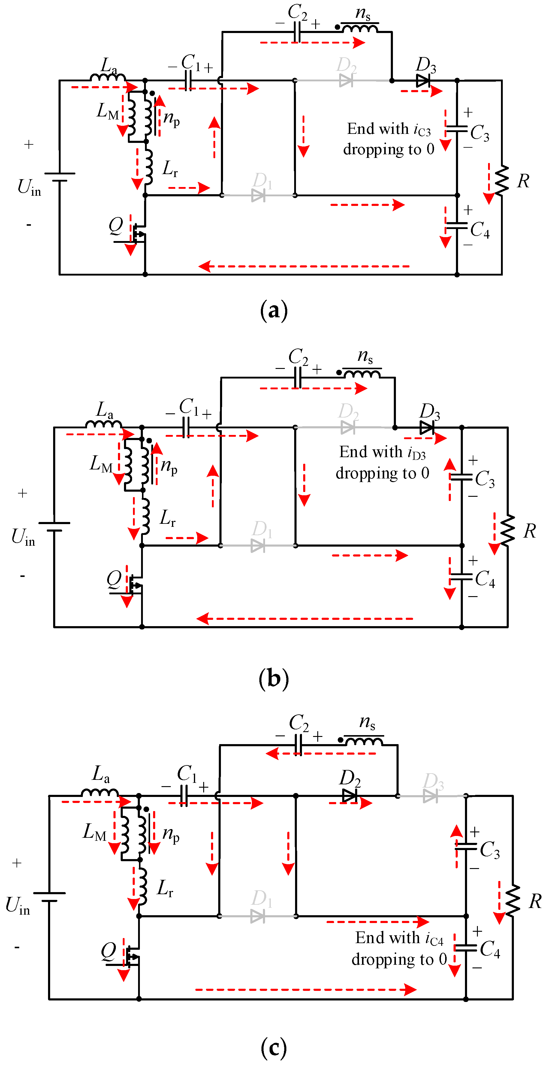
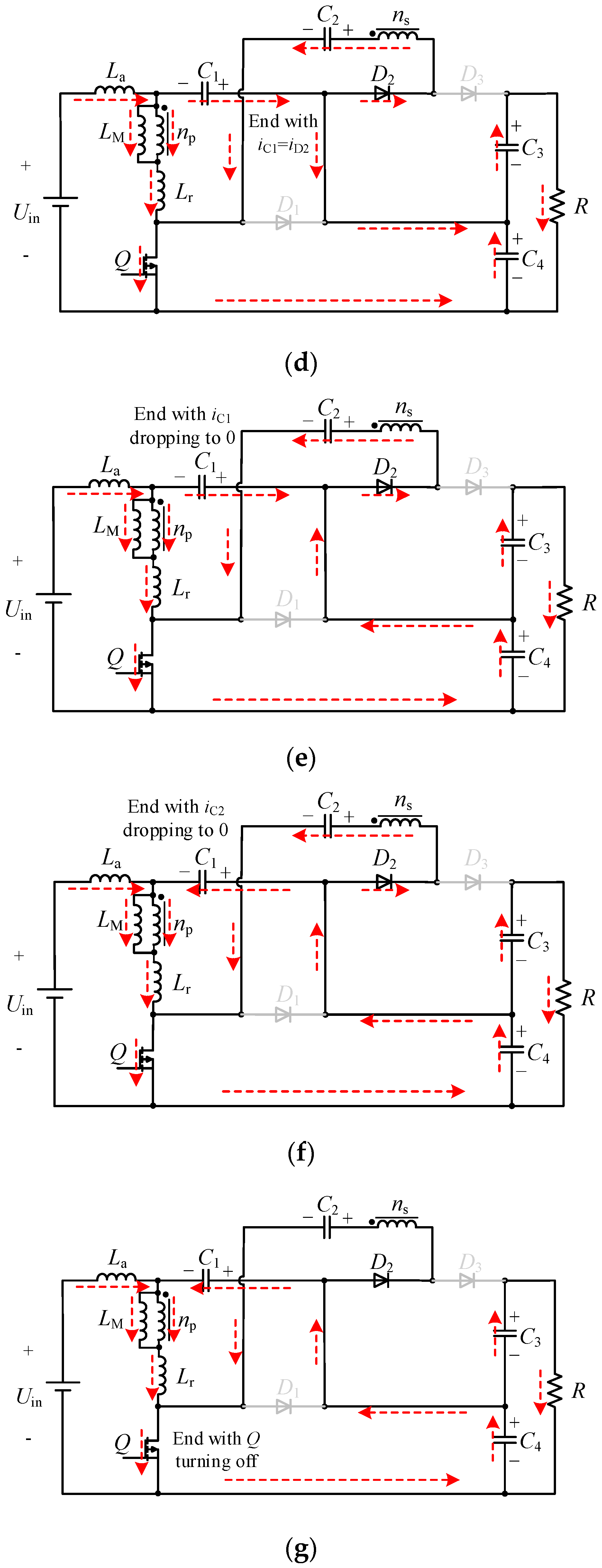
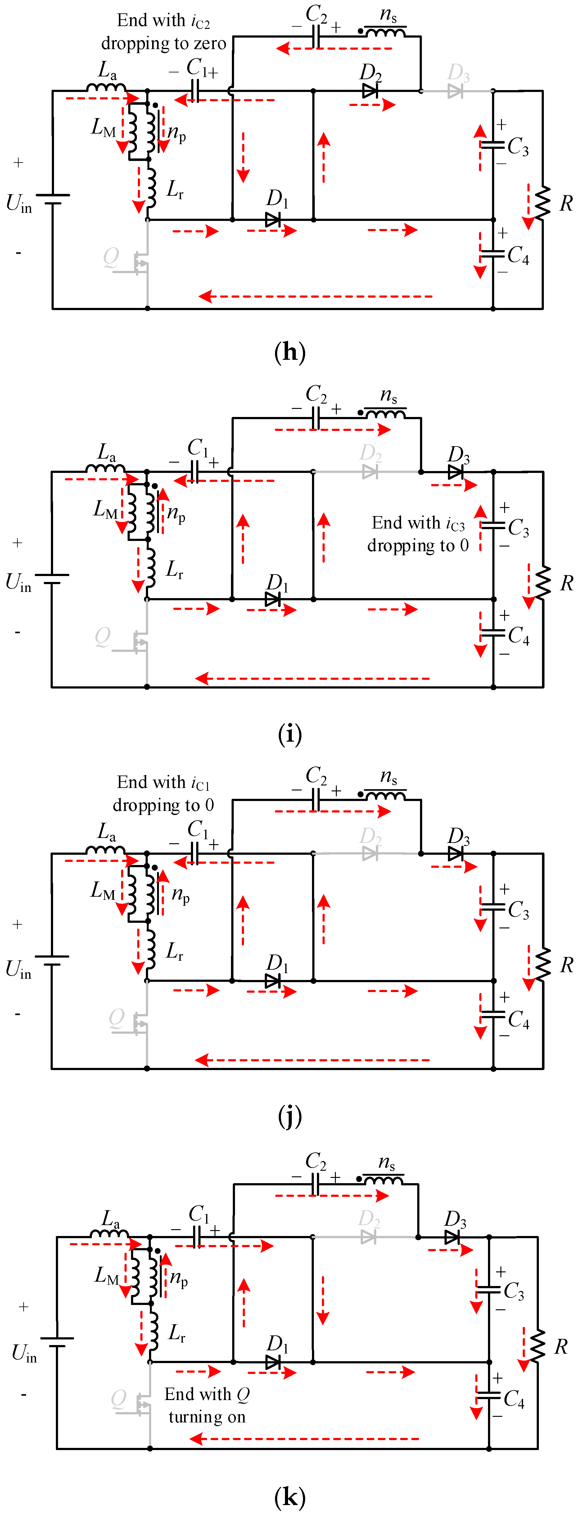
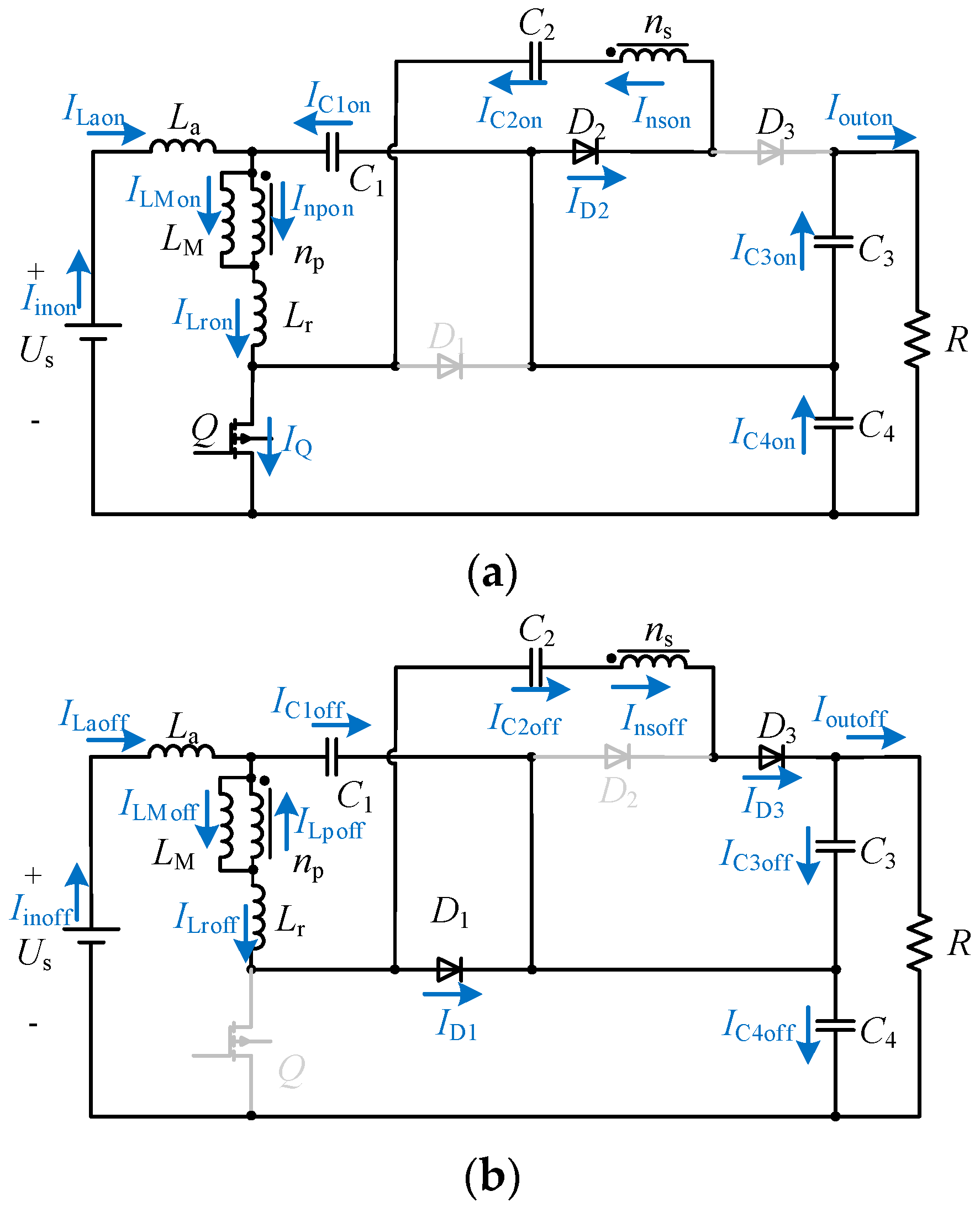
3.1. Operating Principles

The proposed converter has 10 operating modes (in which Mode G and Mode H cannot coexist simultaneously in a single switching period), and the corresponding current flow paths are depicted in Figure 2.
Mode A: The power switch Q is turned on. The currents that flow through both sides of the ideal transformer decrease rapidly. Meanwhile, diode D3 is still conducting, and the current flowing through capacitor C1 starts to decrease. This mode ends when the current flowing in C3 becomes zero.
Mode B: The current flowing into diode D3 is no longer able to provide energy for the load and continues to decrease. Accordingly, capacitor C3 begins to discharge, and the current flowing through it increases. The trends of the currents flowing in other branches of the circuit remain the same. This mode ends when the current flowing through diode D3 decreases to zero.
Mode C: The currents flowing into both sides of the ideal transformer are reversed and gradually increase. Diode D2 is turned on, and capacitor C3 is still discharging. The coupled inductor transfers energy to capacitor C2, and it starts to charge. The capacitor C1 continues to discharge, but its current decreases gradually. Meanwhile, capacitor C4 continues to charge, and its current gradually decreases to zero, at which time this mode ends.
Mode D: The current flowing through capacitor C4 begins to reverse and gradually increase, and C4 begins to discharge. The current flowing through capacitor C1 continuously decreases, while the current flowing in diode D2 rises gradually. This mode ends when the current flowing through capacitor C1 is equal to the current flowing in diode D2.
Mode E: The current flowing in diode D2 continues to increase, and it is larger than the current flowing through capacitor C1. As a result, the current flowing through capacitor C4 continues to rise. When the current flowing into capacitor C1 decreases to zero, this mode ends.
Mode F: Capacitor C1 starts to charge, and the current flowing in it increases gradually. Then the current decreases as the capacitor voltage rises.
Mode G: The charging process of capacitor C2 is completed, and the current flowing in the secondary side of the ideal transformer ns reduces to zero. The current flowing in the primary side np of the ideal transformer increases faster because there is no energy being transferred to the secondary side. This mode does not exist when the duty cycle is small (based on the magnetizing inductor).
Mode H: This mode and Mode G are mutually exclusive, and the converter goes directly into Mode I when Mode G exists. Q is turned off at the beginning, and the magnetizing inductor LM discharges. As a result, the current flowing into the leakage inductance Lr starts to decrease. Because of the conduction of diode D1, the voltage stress across Q is clamped at the voltage across the capacitor C4. The capacitor C4 continues charging. Meanwhile, capacitor C2 is still in the charging state because the currents flowing into both sides of the ideal transformer have not reversed yet. The diode D2 remains turned on, and the current flowing through capacitor C1 begins to decrease. This mode finishes when the current flowing in capacitor C2 reduces to zero.
Mode I: In this mode, the currents flowing into both sides of the ideal transformer reverse and start to increase, and the current flowing into C3 begins to decrease because of the conduction of D3. When the current flowing into C3 decreases to zero, this mode ends.
Mode J: The current flowing into D3 continues to increase, and C3 changes into a charging state. The current trends of other branches remain unchanged. This mode terminates when the current flowing into C1 decreases to zero.
Mode K: C1 begins to discharge, and energy is transferred to C4 from C1. As the current flowing through La does not change, the current flowing into the primary side np falls. As a result, the current flowing into the secondary side ns begins to decrease. This mode terminates when the power switch Q turns on.
Mode F, Mode G, and Mode K have the longest durations of these 10 modes (Mode G and Mode H cannot coexist simultaneously), while the other 7 modes are transient states that last for a very short time. As a result, the simplified current waveforms of the circuit elements in a switching period are given in Figure 3.
According to the states of Mode A–Mode G shown in Figure 2, the relationship between inductors and a current ripple can be obtained as
L M + L a + L r = U in d 2 f α I L
where α is the current ripple coefficient. The output filtering capacitors are chosen to be large enough that the voltage ripples can be limited well. Therefore, the relationship between C4 and its voltage ripple can be obtained as
C 4 Δ i L T s 8 Δ u = α I L T s 8 Δ u

3.2. Analysis of Ripple Minimization Characteristics

Assume that the capacitors and the inductors employed are large enough, and the forward voltage and the on-state resistances of all semiconductors are negligible. The average voltages across C1, C2, C3, and C4 are UC1, UC2, UC3, and UC4 respectively; Uin is the steady input voltage; uLa is the instantaneous inductor voltage; the instantaneous current flowing into La is iLa and the average inductor current is ILa; and the duty cycle is d.
Over the whole switching period, the input inductor La, the capacitor C1, and the capacitor C4 form a closed circuit loop, and the following equation can be derived by applying Kirchhoff’s Voltage Laws (KVLs):
{ u La = u in u C 4 + u C 1 u La = L a d i La ( t ) d t ,
where uin is the instantaneous input voltage, and uc1 and uc4 are the instantaneous voltages across C1 and C4.
Considering the steady state, the inductor La satisfies the voltage second balance principle, and thus the average voltage across the inductor La is zero in each switching period. Therefore, Equation (4) can be obtained. The voltage ripples across C1 and C4 are very close to zero, and the input voltage is regarded as constant in a switching period, so the instantaneous inductor voltage uLa is very small, according to Equation (3). Therefore, the current ripple of the inductor current iLa can be regarded as zero, which means that input current ripple minimization can be realized:
{ U C 1 = U C 4 U in U La = 0 .
It can be seen that the characteristics of current ripple minimization are affected by La, uC1, and uC4. The capacitor voltage fluctuation is smaller if the capacitances of C1 and C4 are larger, which is beneficial to the realization of current ripple minimization.

3.3. Voltage Gain Analysis

In a steady state, neglecting the other transient state modes, the main modes (Mode F, Mode G, and Mode K) are analyzed. In view of the influence of leakage inductance on the voltage gain, the coupling coefficient k = LM/(LM + Lr) is introduced.
When the power switch Q is turned on, the voltage across the primary side np of the ideal transformer is equal to kUin, while the voltage across the secondary side ns is UC2UC4. Equation (5) can be obtained:
n k U in = U C 4 U C 2 .
When the power switch Q is turned off, the voltage across the primary side np is changed to kUC1, and the voltage across the secondary side ns becomes UC3UC2. Therefore, Equation (6) can be obtained:
n k U C 1 = U C 3 U C 2 .
Applying the voltage second balance principle to the magnetizing inductor LM yields Equation (7):
k U in d = k ( U C 4 U in ) ( 1 d ) .
From Equations (4)–(7), the voltages across C1, C2, C3, and C4 can be derived as
{ U C 1 = d 1 d U in U C 2 = n k n k d + 1 1 d U i n U C 3 = n k + 1 1 d U in U C 4 = 1 1 d U in .
Above all, the voltage gain M of the proposed converter can be expressed as
M = U out U in = U C 3 + U C 4 U in = n k + 2 1 d .

3.4. Analysis of Passive Lossless Clamping Circuit

As can be seen in Figure 2h, the diode D1 and the capacitor C4 form a passive lossless clamping circuit. C4 can absorb the energy stored in the leakage inductance through D1 and limit the voltage stress across the power switch Q to UC4. This passive lossless clamping circuit provides a path for transmitting leakage inductance energy to the load. Moreover, it can raise the efficiency of the converter and suppress the voltage spike across the power switch Q caused by leakage inductance Lr.

4. Voltage and Current Stresses and Performance Comparisons

4.1. Voltage Stresses

In view of the analysis of the operating modes, the power switch Q and the capacitor C4 are connected in parallel when Q is turned off, and D2 is connected to the capacitor C3 in parallel when D2 is turned off. In other words, the voltages across Q and C4 are equal, and the voltage stress across D2 is UC3. The voltage stresses across Q and D2 can be derived as
U Q = U C 4 = 1 1 d U in ,
U D 2 = U C 3 = n k + 1 1 d U in .
Similarly, the voltage stress across D1 is UC4 and the voltage stress across D3 is UC3 when Q is turned on. Thus, the voltage stresses across D1 and D3 can be derived as
U D 1 = U C 4 = 1 1 d U in ,
U D 3 = U C 3 = n k + 1 1 d U in .
It can be concluded that the voltage stresses across the power switch Q and the diode D1 are independent of the coupled inductors and are only related to the duty cycle d and the input voltage Uin. The voltage stresses across diode D2 and diode D3 are not only related to d, but are also related to the turns ratio n. Hence, it is beneficial to choose a desired turns ratio n for the coupled inductors to obtain a trade-off between the voltage gain and the voltage stresses across D2 and D3.

4.2. Current Stresses

To simplify the calculation of current stresses, the influence of leakage inductance is neglected, which means k = 1 (see Figure 4). When the power switch Q is turned on, the currents flowing into C1, C2, C3, and C4 are IC1on, IC2on, IC3on, and IC4on; and the current flowing into La is ILaon. Inpon is the current flowing into the primary side of the ideal transformer, while Inson is the current flowing into the secondary side. Meanwhile, the current flowing into LM is ILMon, and the current flowing into Lr is ILron. ID2 is the current of D2. Iinon and Iouton are the input current and the output current, respectively.
When the power switch Q is turned off, the currents flowing into C1, C2, C3, and C4 are IC1off, IC2off, IC3off, and IC4off; the current flowing into La is ILaoff; and the currents flowing into both sides of the ideal transformer are Inpoff and Insoff. ILMoff is the current flowing into LM, and the current flowing into Lr is ILroff. ID1 is the current of D1, while ID3 is the current of D3. The input current and the output current are Iinoff and Ioutoff, respectively.
By applying the ampere second balance principle to C1C4, the equations can be derived as
{ I C 1 on d = I C 1 off ( 1 d ) I C 2 on d = I C 2 off ( 1 d ) I C 3 on d = I C 3 off ( 1 d ) I C 4 on d = I C 4 off ( 1 d ) .
According to Figure 4a, it can be deduced that
{ I C 3 on = I outon I C 1 on + I C 2 on + I C 3 on = I C 4 on I Laon + I C 1 on = I LMon + I npon I npon = n I nson = n I C 2 on .
Similarly, Equation (16) can be derived from Figure 4b:
{ I Laoff = I C 1 off + I LM off I npoff I C 2 off = I C 3 off + I out off I Laoff I out off = I C 4 off I npoff = n I nsoff = n I C 2 off .
Considering that the load is resistive, and the currents flowing into La and LM are assumed to be constant, Equation (17) can be derived:
{ I outon = I outoff = I out I Laon = I Laoff = I La I LMon = I LMoff = I LM .
In terms of Equations (14)–(17), the capacitor currents can be deduced as Equations (18) and (19):
{ I C 1 on = n d I out I C 1 off = n 1 d I out I C 2 on = 1 d I out I C 2 off = 1 1 d I out I C 3 on = I out I C 3 off = d 1 d I out I C 4 on = 1 + n + d d I out I C 4 off = 1 + n + d 1 d I out ,
{ I La = n + 2 1 d I out I LM = n + 2 1 d I out .
The current stresses of the power switch Q and the diode D2 can be obtained according to Figure 4a, Equations (18) and (19):
I Q = I La + I C 4 on I C 3 on = n + 2 d ( 1 d ) d I out ,
I D 2 = I C 2 on = 1 d I out .
Similarly, the current stresses of D1 and D3 can be obtained by means of Figure 4b, Equations (18) and (19):
I D 1 = I La I C 1 off I C 2 off = 1 1 d I out ,
I D 3 = I C 2 off = 1 1 d I out .

4.3. Performance Comparisons

The proposed converter was compared to the converter in Reference [29] without considering the influence of leakage inductance. The specific comparisons are shown in Table 1. The voltage stress across the diode D1 was larger than the output voltage in the converter of Reference [29], while the voltage stresses across all semiconductors in the proposed converter were less than the output voltage. Moreover, the proposed converter could achieve a much higher voltage gain at the cost of one more diode and one more capacitor. The voltage gain M versus the duty cycle d is shown in Figure 5 when the turns ratio n is equal to 1 and 2.

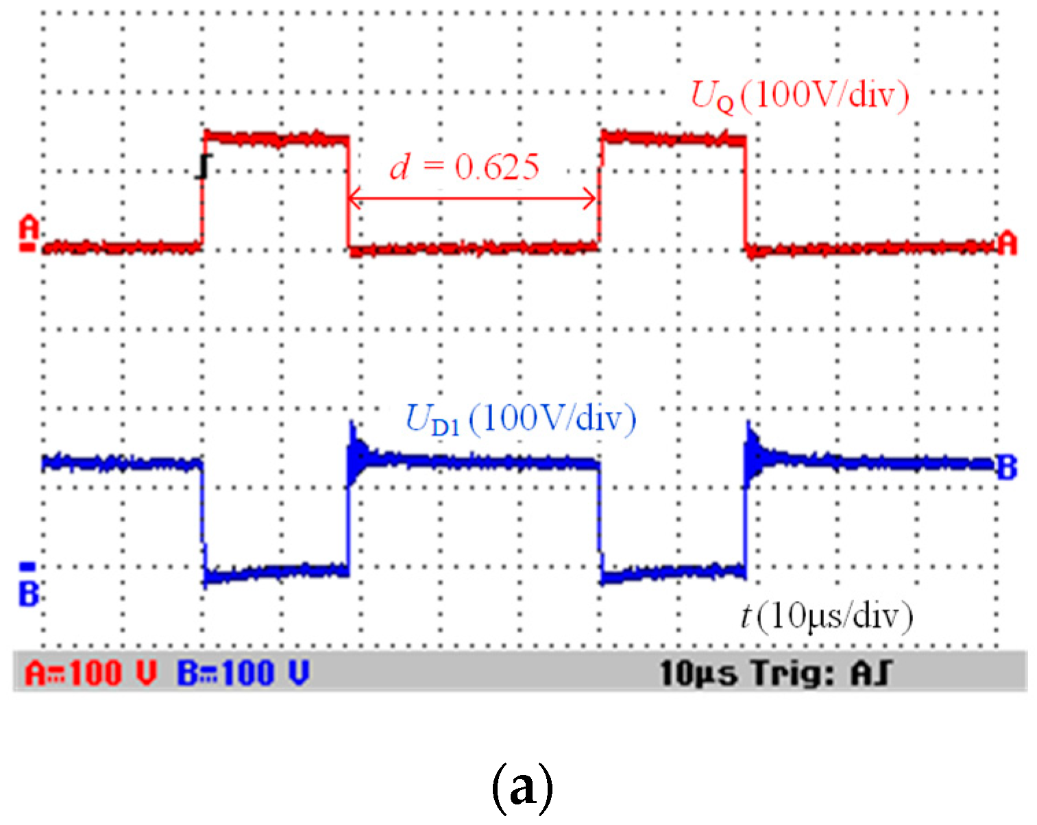
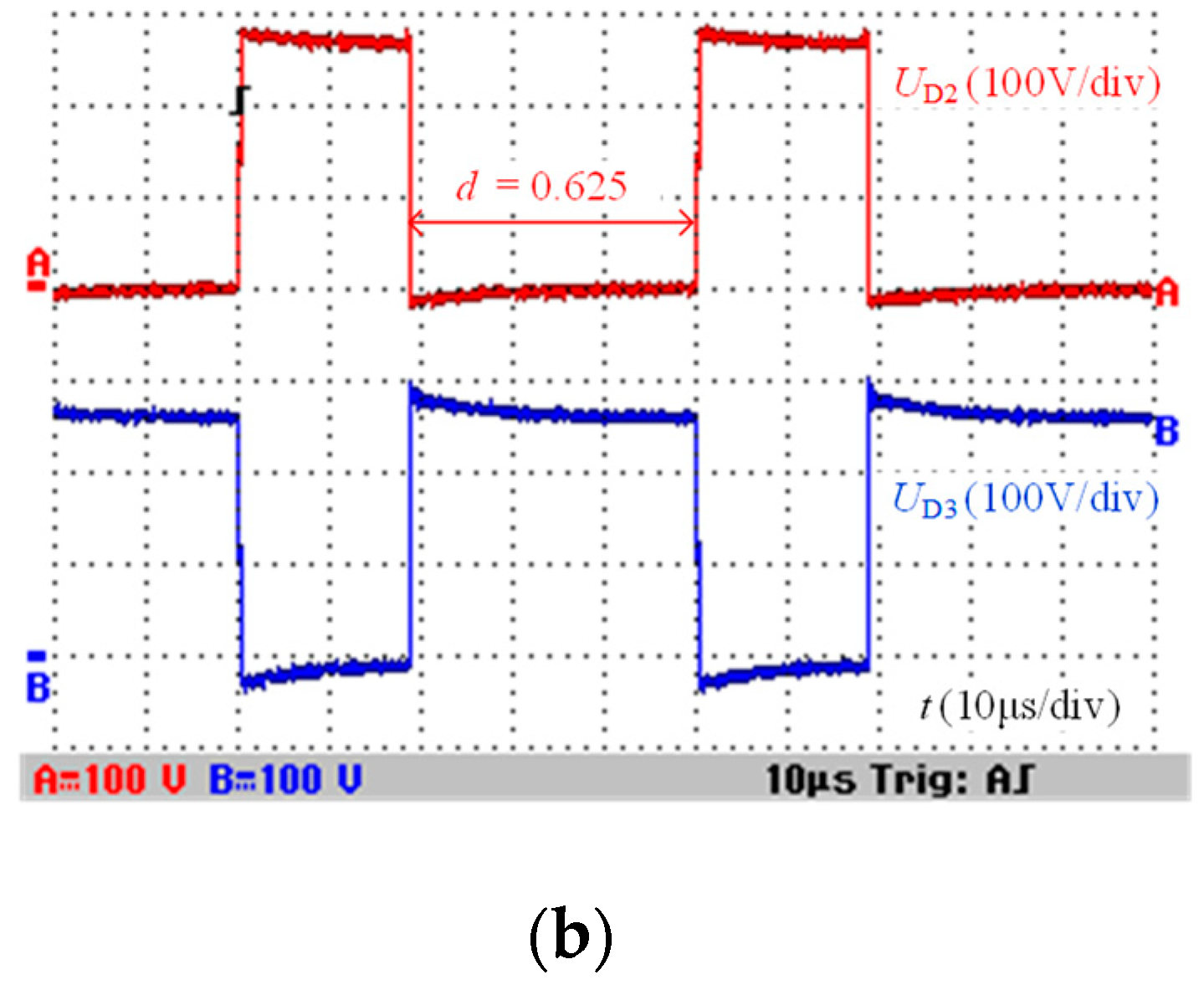
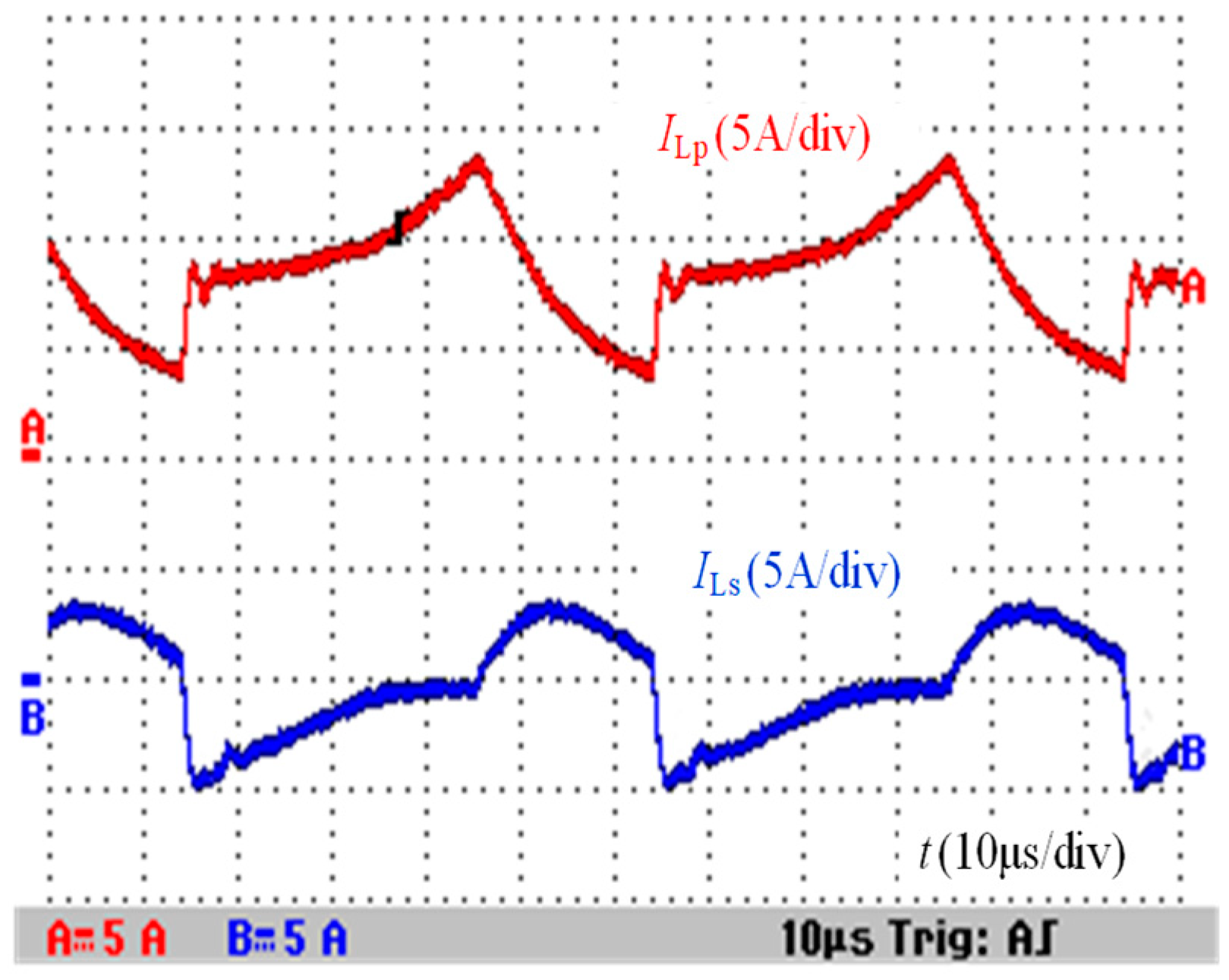
5. Experimental Results and Analysis

In order to validate the feasibility of the proposed converter, a 400-W prototype was developed, as shown in Figure 6. An adjustable DC source with a voltage range of Uin = 30–100 V was used as the input of the converter to simulate a fuel cell source. The output voltage was controlled to 400 V by a voltage loop implemented on a digital signal processor (DSP) TMS320F28335. The experiment parameters are listed in Table 2. According to Equation (1), the current ripple coefficient α is defined as 0.2, and a large La can reduce the input current ripple: Therefore, La and LM were taken as 241 μH and 368 μH, respectively. From Equation (2), the voltage ripple Δu is defined as 0.5 V. Considering practical experience and the laboratory conditions, C2C4 were taken as 540 μF, and C1 was taken as 270 μF.
The voltage stresses across all of the semiconductors for d = 0.625 and Uout = 400V are shown in Figure 7. Figure 7a shows the voltage stresses across Q and D1, which were equal to 133 V, while Figure 7b shows the voltage stresses across D2 and D3, which were 267 V, which was consistent with the theoretical analysis. In addition, the energy stored in the leakage inductance was released through the diode D1 when Q was turned off. As a result, the voltage spike across the power switch Q was reduced significantly. The current flowing into the inductor La and the voltage across the capacitor C1 are shown in Figure 8. The input current Iin, which flowed into La, had no fluctuation in each switching period, and neither did the voltage across C1. Thus, it could be concluded that input current ripple minimization was achieved, as analyzed in Section 3.2. Figure 9 shows the currents flowing into both sides of the coupled inductors. The capacitor C2 received energy from the coupled inductors when Q was turned on. On the contrary, the current ILp flowing into the primary side started to decrease when Q was turned off, C2 started to discharge, and the current ILs flowing into the secondary side transferred energy to the load through D3. The experimental results were consistent with the theoretical analysis.
Figure 10 shows that with the voltage control loop, the output voltage Uout could be kept constant at 400 V, even when the input voltage Uin varied from 30 V to 100 V continuously. This demonstrated that the proposed converter could operate well in a wide voltage gain range from 13.33 to 4.
The efficiencies of the proposed converter with different input voltages and different powers were measured by a power analyzer (YOKOGAWA/WT3000), as shown in Figure 11. When the input voltage Uin = 100 V and the load power P = 400 W, the proposed converter reached a maximum conversion efficiency of 95.12%. The minimum efficiency was 89.24% when the input voltage Uin = 40 V and the load power P = 400 W. To sum up, with the same power, as the voltage gain increased (i.e., the input voltage decreased), the efficiency of the proposed converter decreased. Since the input current rose as the low-side voltage decreased, the copper loss and the switching losses of the converter rose. Therefore, the efficiency of the converter appeared to degrade at a high voltage gain.

6. Conclusions

A coupled-inductor DC-DC converter with a high voltage gain and input current ripple minimization was proposed in this paper. The converter can obtain a wide voltage gain range, and the voltage stresses across all semiconductors are lower than the output voltage. In addition, the proposed converter can benefit from the minimization of input current ripples. Furthermore, the passive lossless clamping circuit effectively suppresses voltage spikes caused by leakage inductance. Therefore, it is a good candidate for the power interface of fuel cell vehicles.

Author Contributions

Conceptualization, Y.Z.; methodology, J.L.; software, C.Z.; validation, C.D.; formal analysis, W.Z.; investigation, F.Y.; resources, F.Y.; data curation, C.Z.; writing—original draft preparation, C.Z. and F.Y.; writing—review and editing, J.L., and W.Z.; visualization, C.D.; supervision, Y.Z.; project administration, Y.Z.; funding acquisition, Y.Z.

Funding

This research was funded by Natural Science Foundation of China, grants number 51577130 and 51207104.

Conflicts of Interest

The authors declare no conflict of interest.

References

  1. Khaligh, A.; Li, Z. Battery, ultracapacitor, fuel cell, and hybrid energy storage systems for electric, hybrid electric, fuel cell, and plug-in hybrid electric vehicles: State of the art. IEEE Trans. Veh. Technol. 2016, 59, 2806–2814. [Google Scholar] [CrossRef]
  2. Bahroon, D.A.; Rahman, H.A. Performance evaluation of solar-fossil fuel-hybrid parabolic trough power plant in Yemen under different fuel types. In Proceedings of the 2014 IEEE Conference on Energy Conversion (CENCON), Johor Bahru, Malaysia, 13–14 October 2014; pp. 158–163. [Google Scholar]
  3. Zeng, B.; Zhang, J.; Yang, X.; Wang, J.; Dong, J.; Zhang, Y. Integrated planning for transition to low-carbon distribution system with renewable energy generation and demand response. IEEE Trans. Power Syst. 2014, 29, 1153–1165. [Google Scholar] [CrossRef]
  4. Boulanger, A.G.; Chu, A.C.; Maxx, S.; Waltz, D.L. Vehicle electri- fication: Status and issues. Proc. IEEE. 2011, 99, 1116–1138. [Google Scholar] [CrossRef]
  5. Li, K.; Chen, T.; Luo, Y.; Wang, J. Intelligent environment-friendly vehicles: concept and case studies. IEEE Trans. Intell. Transp. Syst. 2011, 13, 318–328. [Google Scholar] [CrossRef]
  6. Jin, J.X.; Chen, X.Y.; Wen, L.; Wang, S.C.; Xin, Y. Cryogenic power conversion for SMES application in a liquid hydrogen powered fuel cell electric vehicle. IEEE Trans. Appl. Supercond. 2015, 25, 1–11. [Google Scholar]
  7. Su, W.; Rahimi-Eichi, H.; Zeng, W.; Chow, M.-Y. A survey on the electrification of transportation in a smart grid environment. IEEE Trans Ind. Informat. 2012, 8, 1–10. [Google Scholar] [CrossRef]
  8. Jiang, W.; Fahimi, B. Active current sharing and source management in fuel cell-battery hybrid power system. IEEE Trans. Ind. Electron. 2010, 57, 752–761. [Google Scholar] [CrossRef]
  9. Restrepo, C.; Konjedic, T.; Guarnizo, C.; Aviñó-Salvadó, O.; Calvente, J.; Romero, A.; Giral, R. Simplified mathematical model for calculating the oxygen excess ratio of a PEM fuel cell system in real-time applications. IEEE Trans. Ind. Electron. 2014, 61, 2816–2825. [Google Scholar] [CrossRef]
  10. Rathore, A.K.; Bhat, A.K.S.; Oruganti, R. Analysis, design and experimental results of wide range ZVS active-clamped L-L type currentfed DC-DC converter for fuel cell to utility interface application. IEEE Trans. Ind. Electron. 2012, 59, 473–485. [Google Scholar] [CrossRef]
  11. Jang, M.; Agelidis, V.G. A boost-inverter-based, battery-supported, fuel-cell sourced three-phase stand-alone power supply. IEEE Trans. Power Electron. 2014, 29, 6472–6480. [Google Scholar] [CrossRef]
  12. Tseng, K.C.; Lin, J.T.; Huang, C.C. High step-up converter with three-winding coupled inductor for fuel cell energy source applications. IEEE Trans. Power Electron. 2015, 30, 574–581. [Google Scholar] [CrossRef]
  13. Wang, P.; Zhao, C.; Zhang, Y.; Li, J.; Gao, Y. A bidirectional three-level dc-dc converter with a wide voltage conversion range for hybrid energy source electric vehicles. J. Power Electron. 2017, 17, 334–345. [Google Scholar] [CrossRef]
  14. Qian, W.; Cao, D.; Cintron-Rivera, J.G.; Gebben, M.; Wey, D.; Peng, F.Z. A switched-capacitor DC-DC converter with high voltage gain and reduced component rating and count. IEEE Trans. Ind. Appl. 2012, 48, 1397–1406. [Google Scholar] [CrossRef]
  15. Wu, B.; Li, S.; Smedley, K.; Singer, S. A family of two-switch boosting switched-capacitor converters. IEEE Trans. Power Electron. 2015, 30, 5413–5424. [Google Scholar] [CrossRef]
  16. Wai, R.J.; Duan, R.Y. High step-up converter with coupled-inductor. IEEE Trans. Power Electron. 2005, 20, 1025–1035. [Google Scholar] [CrossRef]
  17. Yang, L.S.; Liang, T.J.; Lee, H.C.; Chen, J.F. Novel high step-up DC-DC converter with coupled-inductor and voltage-doubler circuits. IEEE Trans. Ind. Electron. 2011, 58, 4196–4206. [Google Scholar] [CrossRef]
  18. Ajami, A.; Ardi, H.; Farakhor, A. A novel high step-up DC/DC converter based on integrating coupled inductor and switched-capacitor techniques for renewable energy applications. IEEE Trans. Power Electron. 2015, 30, 4255–4263. [Google Scholar] [CrossRef]
  19. Dwari, S.; Parsa, L. An efficient high-step-up interleaved DC-DC converter with a common active clamp. IEEE Trans. Power Electron. 2011, 26, 66–78. [Google Scholar] [CrossRef]
  20. Zhao, Y.; Li, W.; Deng, Y.; He, X. High step-up boost converter with passive lossless clamp circuit for non-isolated high step-up applications. IET Trans. Power Electron. 2011, 4, 851–859. [Google Scholar] [CrossRef]
  21. Thounthong, P.; Sethakul, P.; Davat, B. Modified 4-phase interleaved fuel cell converter for high-power high-voltage applications. In Proceedings of the 2009 IEEE International Conference on Industrial Technology, Gippsland, VIC, Australia, 10–13 February 2009. [Google Scholar]
  22. Hu, X.; Gong, C. A high gain input-parallel output-series DC/DC converter with dual coupled inductors. IEEE Trans. Power Electron. 2015, 30, 1306–1317. [Google Scholar] [CrossRef]
  23. Tan, S.-C.; Kiratipongvoot, S.; Bronstein, S.; Ioinovici, A.; Lai, Y.M.; Tse, C.K. Adaptive mixed on-time and switching frequency control of a system of interleaved switched-capacitor converters. IEEE Trans. Power Electron. 2011, 26, 364–380. [Google Scholar] [CrossRef]
  24. Tseng, K.-C.; Huang, C.-C. High step-up high-efficiency interleaved converter with voltage multiplier module for renewable energy system. IEEE Trans. Ind. Electron. 2014, 61, 1311–1319. [Google Scholar] [CrossRef]
  25. Zhan, Y.; Guo, Y.; Zhu, J.; Li, L. Performance comparison of input current ripple reduction methods in UPS applications with hybrid PEM fuel cell/supercapacitor power sources. Int. J. Electr. Power Energy Syst. 2015, 64, 96–103. [Google Scholar] [CrossRef]
  26. Zhan, Y.; Guo, Y.; Zhu, J.; Li, L. Input current ripple reduction and high efficiency for PEM fuel cell power conditioning system. In Proceedings of the 2017 20th International Conference on Electrical Machines and Systems (ICEMS), Sydney, NSW, Australia, 11–14 August 2017. [Google Scholar]
  27. Paja, C.A.R.; Arango, E.; Giral, R.; Montesa, A.J.S.; Carrejo, C. DC/DC pre-regulator for input current ripple reduction and efficiency improvement. Elect. Power Syst. Res. 2011, 81, 2048–2055. [Google Scholar] [CrossRef]
  28. Shi, Y.; Liu, B.; Duan, S. Low-frequency input current ripple reduction based on load current feedforward in a two-stage single-phase inverter. IEEE Trans. Power Electron. 2016, 31, 7972–7985. [Google Scholar] [CrossRef]
  29. Chen, Z.; Xu, J. High boost ratio DC-DC converter with ripple-free input current. Electron. Lett. 2014, 50, 353–355. [Google Scholar] [CrossRef]
Figure 1. The proposed coupled-inductor DC-DC converter. (a) The topology; (b) the equivalent circuit.
Energies 12 01689 g001
Figure 2. Current flow paths of the proposed converter in one switching period. (a) Mode A; (b) Mode B; (c) Mode C; (d) Mode D; (e) Mode E; (f) Mode F; (g) Mode G; (h) Mode H; (i) Mode I; (j) Mode J; (k) Mode K.
Energies 12 01689 g002aEnergies 12 01689 g002bEnergies 12 01689 g002c
Figure 3. The simplified current waveforms of the converter. Mode A: End with iC3 dropping to 0; Mode B: End with iD3 dropping to 0; Mode C: End with iC4 dropping to 0; Mode D: End with iC1 equaling iD2; Mode E: End with iC1 dropping to 0; Mode I: End with iC3 dropping to 0; Mode J: End with iC1 dropping to 0.
Energies 12 01689 g003
Figure 4. The current distribution in different states: (a) Q is turned on; (b) Q is turned off.
Energies 12 01689 g004
Figure 5. Curves of voltage gain versus duty cycle for two types of converters with input current ripple minimization.
Energies 12 01689 g005
Figure 6. The experimental prototype of the proposed converter.
Energies 12 01689 g006
Figure 7. Voltage stresses across all semiconductors when Uin = 50 V and Uout = 400 V: (a) Voltage stresses across Q and D1; (b) voltage stresses across D2 and D3.
Energies 12 01689 g007aEnergies 12 01689 g007b
Figure 8. The current flowing into the inductor La and the voltage across the capacitor C1.
Energies 12 01689 g008
Figure 9. The currents flowing into both sides of the coupled inductor.
Energies 12 01689 g009
Figure 10. The output voltage and the wide-range input voltage from 30 V to 100 V.
Energies 12 01689 g010
Figure 11. Efficiencies of the proposed converter with different output powers at different input voltages (i.e., different voltage gains) when Uout = 400 V.
Energies 12 01689 g011
Table 1. Comparisons of two types of converters with input current ripple minimization.
CharacteristicsConverter in [29]Proposed Converter
Voltage Gain ( n d + 1 ) / ( 1 d ) ( n + 2 ) / ( 1 d )
Voltage Stress of power switch 1 1 d U in 1 1 d U in
Voltage Stress of diodes D C : 1 1 d U in D 1 : 1 1 d U in
D 1 : n + 1 1 d U in D 2 , D 3 : n + 1 1 d U in
Current Stress of power switch n d + 1 ( 1 d ) d I out n + 2 d ( 1 d ) d I out
Current Stress of diodes D C : n d + 1 2 ( 1 d ) d I out D 1 , D 3 : 1 1 d I out
D 1 : n d + 1 ( 1 d ) d I out D 2 : 1 d I out
Number of power switches11
Number of diodes23
Ripple-minimization input currentYesYes
Table 2. Experiment parameters.
ParametersValues
Rated power Pn400 W
Switching frequency fs20 kHz
Capacitor C1270 μF
Capacitors C2, C3, and C4540 μF
Inductor La241 μH
Magnetizing inductor LM368 μH
Leakage inductance Lr3.25 μH
Turns ratio np:ns1:1
Output voltage Uout400 V
Input voltage Uin30–100 V
Power switch QIXTH88N30P
Diodes D1D3DPG60C300HB

