Abstract
A new structure of switched capacitor multilevel inverter (SCMLI) capable of voltage boosting and with self-balancing ability is introduced in this article. This advantage is the result of a step by step rise of capacitor voltages in each module, supplied by just one DC voltage source. The proposed topology generates a sinusoidal output waveform with a magnitude several times greater than the input one. Higher output staircase AC voltage is obtained by applying a nearest level control (NLC) modulation technique. The most significant features of this configuration can be mentioned as: fewer semiconductor devices, remarkably low total harmonic distortion (THD), desirable operating under high/low frequency, high efficiency, inherent bipolar voltage production, easy circuit expansion, ease of control and size reduction of the circuit thanks to utilizing neither bulky transformer nor inductor. Moreover, the proposed SCMLI is comprehensively surveyed through theoretical investigation and a comparison of its effectiveness to recent topologies. Eventually, the operating principle of a 25-level prototype of the suggested SCMLI is validated by simulation in the MATLAB SIMULINK environment and experimental results.
1. Introduction
The growth of energy consumption and reduction in fossil fuel reserves has led to renewable energy penetration in power system. In order to transmit the electricity generated by these sources to grids, power electronic devices are widely required. Hence, the noticeable role of power electronic converters in these applications have attracted the attention of many researchers aiming for augmentation of quality, efficiency and costs of such systems [1]. Among all kinds of power electronic converters, inverters are vitally required in such equipment. According to [2], the necessity of high voltage and high power inverters are significantly observed in bulk power controls.
Initial inverters, built in three-level topologies, suffered from high voltage stresses and total harmonic distortion (THD) [3]. Consideration of these limitations, resulted in the introduction of the multilevel inverter (MLI). These inverters are considered favorably for their special characteristics in less THD, lower dv/dt stress, better electromagnetic compatibility and of course lower switching losses [3,4,5]. Quality improvement of output voltage wave form depends on the number of voltage levels in multilevel inverters (the greater the output voltage level, the greater the sinusoidal wave form). Based on the quality and type of source and high/medium power demand of circuit, different topologies for multilevel inverters are presented. These inverters are widely implemented in devices used daily such as ac motor equipment (like ac fans, mills, conveyers and pumps) which are commonly utilized in metal, power, oil and gas, water, mining, marine and chemistry industries [6].
The most applicable MLI topologies can be named as neutral point clamp (NPC) [7], flying capacitor (FC) [8], cascade H-bridge (CHB) [9] and switched capacitor (SC) [10] arrangement inverters. Each topology has its own weaknesses that made it necessary to introduce newer structures. For example, NPC and FC suffer from voltage balancing in their DC link capacitors due to their limited switching states. In CHB topology, the requirement of several DC sources causes considerable increase in the cost and size of the inverter.
Among these, the SC is more utilized in power electronic devices, thanks to its less source requirement (single DC source) and boosting capability with no need of any transformers or inductors and ease of controllability. The performance of SC inverter is summarized in charging several capacitors and then discharging them over the load in a predetermined pattern to make a staircase near the sinusoidal voltage. The output voltage amplitude is several times bigger than the input source depending on the structure and number of capacitors included. Recently, these topologies are used in applications such as: lasers, radars, X-rays [11], fuel-cell systems [12], UPS (uninterruptible power supplies) [13], White Light Emitting Diode (WLED), LCD drivers, fluorescent lamp [14], electrical vehicles [15], mobile equipment [16], Induction heating [17], grid integration of renewable energy systems [18], high-frequency AC micro grids [19], high-frequency AC power distribution systems [20], high-frequency-link DC transformers for a Medium Voltage Direct Current (MVDC) power distribution [21] and MRI (Magnetic Resonance Imaging) [22].
A new single-source multi-level inverter (MLI) based on the SC concept with the minimum number of switches is proposed by [23]. Reference [24] proposed another SC-based MLI. In this structure, not only is there no inductors but also larger voltage than the input one is produced. This increase is reached by connecting the capacitors in a series or parallel fashion. On the other hand, introducing two new MLIs consisting of SC units and H-bridges is presented by [25]. A single source SC-based MLI which makes it possible to reach several output levels is introduced by [26]. A different number of output levels is accessible by changing the number of SC cells. References [27,28] introduce new single-source switched capacitor multilevel inverter (SCMLI) structures producing high output voltage levels, aiming for reduction of both active and passive components. Considering power loss analysis is another noticeable aspect of these studies that further discussion over circuit loss is fundamentally investigated in [29,30].
Producing a 5-level output with 7 switches based on the SCMLI technique is presented in [31]. This structure is single source and requires 2 capacitors. Similarly, references [32,33] SC-based topologies are fed by one source aiming to boost the input voltage.
The presented article reveals a new single-source SCMLI topology, which is expected to operate in both high power and high voltage applications. In Section 2 the topology of proposed new SCMLI module and its cascaded structure is described. In Section 3 the operating principles of this topology is discussed. A comprehensive discussion on the proposed topology and others with similar criteria is performed in Section 4. Then, in Section 5, first, simulation results are presented and then experimental tests of the proposed topology are undertaken in the laboratory environment to verify the proposed inverter performance. Finally, Section 6 is devoted to the conclusion of this paper.
2. Proposed Topology
The structure of proposed SCMLI consists of two different parts which are connected one after another to achieve the desired performance (Figure 1). Each part consists of several switches and capacitors in order to generate predetermined voltage levels. The first part includes four capacitors and 14 switches (including 6 unidirectional and 4 bidirectional ones) controlled by 10 driver circuits.
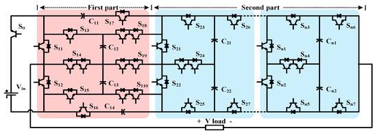
Figure 1.
The overall structure of the proposed switched capacitor multilevel inverter (SCMLI).
Notice that the connection of two switches one after another form a unit to control the current flow bi-directionally. The topology is capable of generating 9 voltage levels containing 4 positive levels, 4 negative levels and a zero level. While the first part is made of one main module, the second part can be made by combining one or more sub-modules together. Each sub-module is made up of 2 capacitors and 8 switches (including 6 unidirectional and 1 bidirectional). By implementing 7 driver circuits, 5 different voltage levels (consist of 2 positive, 2 negative and a zero one) are achievable in each sub-module. Eventually, the predefined output voltage is achieved by combination of the two parts, which the number of sub-modules in the second part fundamentally depends on the desired output level.
3. Operating Principles
Figure 2 shows a 25-level prototype based on the proposed structure which consist of the main module and one sub-module in the second part. The output staircase waveform includes 12 positive, 12 negative and the zero level where each level is reached by synthesizing the different capacitors voltages. It is noticeable that, generating the required staircase waveform can be achieved considering the fact that all capacitors should be charged to the predetermined voltage. Besides, the limitation of rated voltage of the semiconductor devices must be taken into account during charge and discharge.
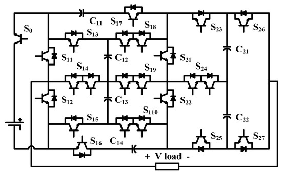
Figure 2.
A 25-level prototype based on the proposed SCMLI structure.
To reach the aforementioned essentials, specific switching patterns for capacitors charging and discharging should be considered.
3.1. Capacitors Charging Pattern
Achieving the favorable voltage waveform requires predetermined charging paths for the capacitors. To reach this goal, the initial step is to charge the capacitors placed in the first part (main module). Regarding Figure 3a capacitor C12 is charged directly by the input source via S0, S12, S13 and S14 switches up to Vin. Similarly, C13 is supplied by the source up to Vin via S0, S11, S14 and S15 switches (Figure 3b). Then, capacitors C11, C14 are charged to the 2Vin voltage by the serial connection of C12 and C13 (Figure 3c,d).
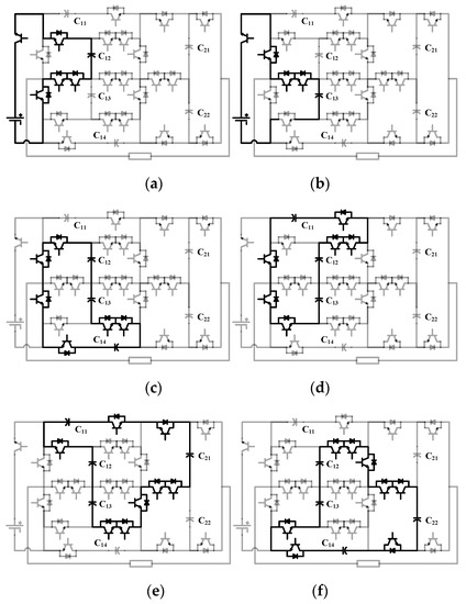
Figure 3.
Capacitors charging paths for proposed SCMLI introduced in Figure 2 for (a) C12; (b) C13; (c) C14; (d) C11; (e) C21; (f) C22.
The next step is to charge the capacitors of the second part (the sub-module) by the serial combination of the capacitors voltages from the previous part. As shown in Figure 3e,f, by using 5 switches and 3 anti-parallel diodes, C21 and C22 are charged to 4Vin. Then, for rest of the modules, two different approaches could be considered. This is either to charge all the other modules with the same voltage, or keep on multiplying (doubling) the capacitor voltages in each step. As a result, for an n-module structure the charging mode for the first and second method could be indicated by and respectively. Choosing each method depends on the amplitude of the input source, required output voltage level and the rated values of the semiconductors.
3.2. Output Multilevel Generation
The selected switching states for charge and discharge of the capacitors for the proposed SCMLI introduced in Figure 2 are brought in Table 1. Besides, the state of charge for each capacitor is shown by either ↑, ↓ or – representing charging, discharging and no change, respectively. As the main module requires 10 gate signals for its 14 switches, then its switching state consists of a 10-digit binary number (including 0 and 1), which 1 means that the corresponding switch in the defined row is in ON state and 0 means that it is in OFF state. Moreover, the switching state of the submodule consists of a 7-digit number. To simplify the demonstration, we separated this 17-digit number into 4-digit parts and turned them from binary to hexadecimal numbers. Then, each switching state is revealed by a 5-digit hexadecimal vector as S = (S0, S11, m11, m12, m21, m22). Where each term means m11 = (S12, S13, S14, S15), m12 = (S16, S17, S18, S19), m21 = (S110, S21, S22, S23), m 22 = (S24, S25, S26, S27).

Table 1.
Selected switching states for charge and discharge of the capacitors (state of charge).
Figure 4 illustrates a few selected discharging paths related to the switching states of Table 1 resulting in a specific mixture of multiple capacitors shaping the staircase output voltage.
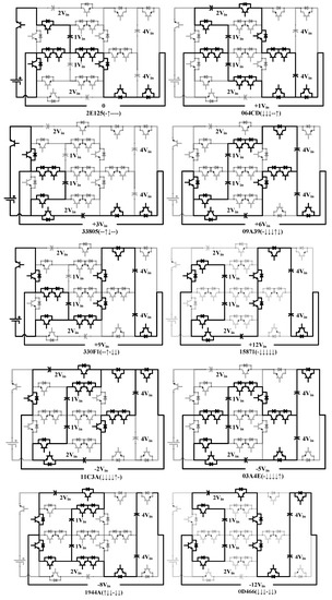
Figure 4.
A few selected discharging paths related to the switching states of Table 1.
3.3. Modulation Strategy
The NLC (nearest level control) technique is utilized for operation of the proposed SCMLI in order to generate the desired staircase voltage. This method generates voltage level by converting the nearest voltage level (Vnl) to the predetermined voltage reference (Vref) [29]. Implementation of this technique not only leads to augmentation of process speed but also eases the calculations by its conceptual and implementation simplicity.
Furthermore, small voltage steps beside low switching frequency allowance makes this technique one of the most suitable methods for high level MLIs. Considering mentioned options, proper switching states could be adapted for each voltage level by the help of switching table (see Table 1). As it is shown in Figure 5, initially the waveform is formed by comparing the Vref and desired output voltage waveform. Then the Vnl can be determined with:
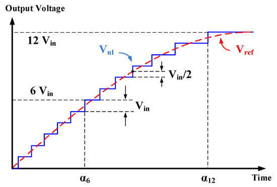
Figure 5.
The operation schematic of the nearest level control (NLC) method.
3.4. Calculations of the Capacitances
To prevent capacitors undercharging and maintaining their voltage ripple in an acceptable range, the capacitances should be determined carefully in the SCMLI topologies. Two main factors should be considered while calculating the circuit capacitances: (1) amplitude of the output current and the phase difference between output voltage and current (2) capacitors discharging time in the worst case. Therefore, maximum discharging of each capacitor can be calculated as [24]:
where fo is fundamental output frequency and Iout is the amplitude of the output current. [t1i, t2i] is the longest discharging period for each capacitor to demonstrate the worst case. Notice that each pair of (C12, C13), (C11, C14) and (C21, C22) have the same capacitance values.
Considering k as the maximum acceptable voltage ripple, the equivalent capacitance of the circuit while supplying the load is obtained as:
As the capacitors C12 and C13, are charged directly by the input source (see Figure 3a,b), thus their voltage is equal to:
Considering p percent tolerance for voltage drop while charging each capacitor, C11 and C14 are charged by series combination of C12 and C13 (see Figure 3c,d). Thus their voltage would be calculated as:
Meaning that . Also the voltages across C12 and C13 would decrease to , unless they are charged again by the DC source. Consequently C11 is obtained by . Finally, C21 and C22 are charged by series combination of either C11, C12 and C13 or C14, C12 and C13 (see Figure 3e,f) up to:
Which means that . Afterwards, in order to transfer the voltage of each sub-module to the next one properly with minimum possible voltage drop, the capacitance values in each sub-module should be times of the previous one. By knowing the value of Ceq and the aforementioned equations, the exact value of every capacitor can be obtained.
4. Discussion
This section presents a discussion on the proposed topology, including two parts: comparison of the proposed structure with a few existing ones, and determination of losses and efficiency.
4.1. Comparison
Table 2 reveals a comprehensive study on the proposed SCMLI structure and six others, for a (2N + 1) level output voltage. The study is categorized into seven parts considering: number of active switches, series diodes, capacitors, driver circuits, the ability to produce bipolar output, peak inverse voltage (PIV) and total standing voltage (TSV).
Table 2.
Comparison of the Suggested SCMLI with six other topologies for a (2N + 1) level output.
The comparison results are illustrated in Figure 6. As shown in Figure 6a, in terms of the semiconductor devices the presented SCMLI utilizes much less active switches and diodes to produce the same output voltage. One may note that [26] needs less active switches, but it is important that [26] uses two series diodes to generate each voltage level. Figure 6b in which the aforementioned topologies are compared in terms of number of capacitors involved in their circuit, implies that the presented topology requires less than 10 capacitors to produce high level output voltages thanks to its multiplying characteristic.
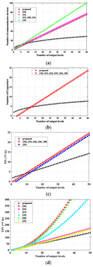
Figure 6.
Comparison results of Table 2 in terms of (a) number of semiconductor devices (b) number of capacitors (c) peak inverse voltage (PIV) (d) total standing voltage (TSV).
It is noteworthy that unlike most other SCMLIs, the proposed concept requires no auxiliary circuit like H-bridge to generate a bipolar voltage. A closer look at Figure 6c reveals that the suggested topology can operate by using semiconductor devices with lower ratings, consequently reducing the total cost of the circuit. In addition, having the lowest amount of the TSV (see Figure 6d) makes the proposed structure suitable for high-voltage applications.
4.2. Determination of Losses and Efficiency
Total circuit loss fundamentally depends on two important sources namely switching and conduction losses [30]. Switching loss enrolls the most important part of circuit loss caused by switching delays which are semiconductor devices inherent characteristics. This source of loss occurs in the course of turning ON and OFF of the active switches determined by the following Equations [27]:
Note that in these equations, fsw represents the switching frequency of each switch of the circuit, stands for the off-state voltage of ith switch, is the current of ith switch when the switch is entirely turned on, and shows the current of ith switch before turning off. Therefore, overall switching loss of the whole circuit can be obtained from the following equation:
Consider that Non(i) and Noff(i) are the number of times which ith switch turns on and off, throughout one cycle. On the other hand, conduction loss is basically generated due to current of semiconductors and hence the load. This loss is calculated by [29]:
where iav-L and irms-L are average and RMS current of voltage level L, respectively. Coefficients k1 and k2 are the number of switches and diodes involved in each level, respectively. Finally, total conduction losses can be calculated as:
Efficiency (η) is obtained from:
where Ploss includes switching losses (Psw) and conduction losses (Pcon). For the proposed SCMLI with , , and using IRF740MOSFET switches, exact calculations were made and the efficiency reached to 92.63%. It is worth highlighting that in the proposed topology of this article the fsw is considerably lower than conventional structures (in the range of 50 Hz up to 1 KHz). Consequently, achieving both lower switching loss and total circuit loss is accessible.
Moreover, in Table 3 the proposed inverter has been compared with other recently introduced topologies in terms of the efficiency. The results depict that the proposed converter not only has the least possible number of components (including active switches with lower TSV, drivers and capacitors), but also enjoys higher efficiency under different load conditions.
Table 3.
Comparison of the proposed topology with other recently introduced ones in terms of efficiency.
The overall efficiency of the proposed 25-level converter is investigated experimentally and theoretically with different loadings as depicted in Figure 7. As can be seen, the lower efficiencies have been recorded by increasing the output power. These high-efficiency values occurred as a result for the few involved components in the current flow paths. The measured efficiencies are in good agreement with theoretical ones.
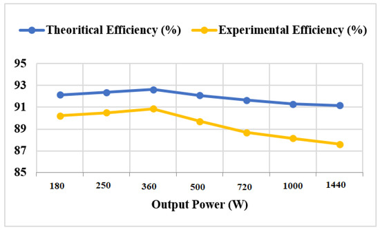
Figure 7.
The overall efficiency of the proposed inverter for different output powers.
5. Results
Evaluation of the proposed theory is comprehensively accomplished in both simulation and experimental sections which are exclusively explained in the following parts.
5.1. Simulation Results
In order to prove the concept of the presented structure, MATLAB simulations were done on a 25-level (30 volts each level) inverter of the proposed topology, using NLC modulation. Figure 8a shows the output voltage and current waveforms for an input of 30 volts (DC) and a resistive load of R = 180 Ω.
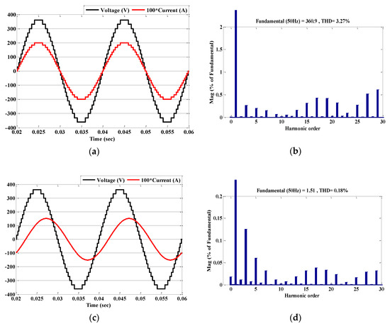
Figure 8.
Simulation results of a 25-level inverter of the proposed topology: (a) output waveforms of a resistive load (R = 180 Ω); (b) fast Fourier transform (FFT) analysis on the output voltage; (c) output waveforms of a resistive-inductive load (R = 180 Ω, L = 500 mH); (d) FFT analysis on the load current.
It is worth noting that the amplitude of the output voltage is 12 times the input. The FFT (fast Fourier transform) of the load voltage is illustrated in Figure 8b. This reveals that the amount of Voltage THD is 3.27% and the amplitude of all voltage harmonics are below 0.6% of the fundamental one.
5.2. Experimental Results
In order to validate the simulation results, a laboratory prototype of a 25-level inverter of the presented SCMLI is made. Figure 9 shows the test setup which is fabricated using the parameters of Table 4.
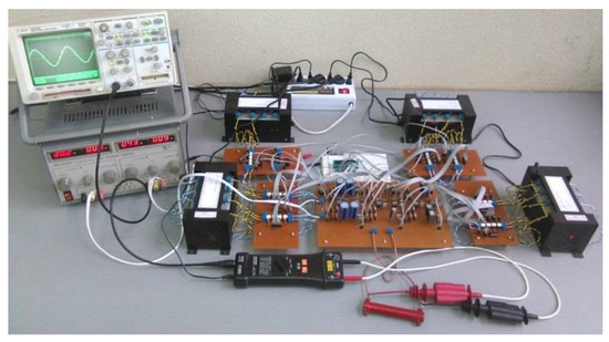
Figure 9.
Laboratory test setup of a 25-level inverter of the presented SCMLI.
Table 4.
Laboratory setup specifications.
Figure 10a,b illustrate the experimental results of the test setup, for a pure resistive load of R = 180 Ω. The voltage and current waveforms comprise 25 steps from peak to peak (each of 30 volts). Note that the voltage probe is set on 100:1 ratio. In addition, test results of a resistive-inductive load (R = 180 Ω, L = 50 mH) with a power factor of 0.75 is brought in Figure 10c,d.
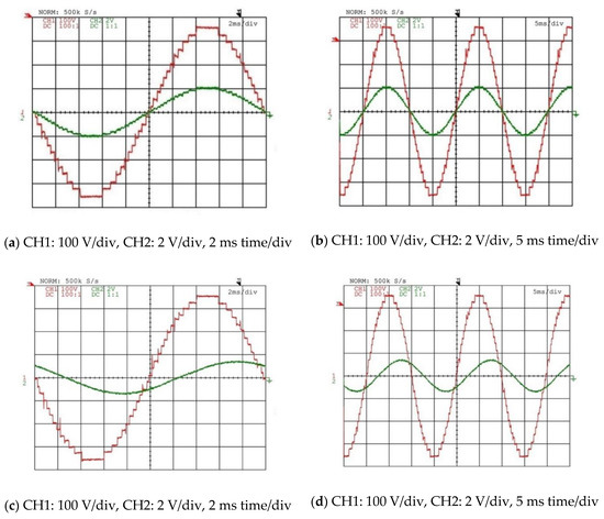
Figure 10.
Experimental results of the proposed SCMLI: (a) R load (2 ms time/div); (b) R load (5 ms time/div); (c) RL load with a power factor of 0.75 (2 ms time/div); (d) RL load with a power factor of 0.75 (5 ms time/div).
6. Conclusions
The introduced novel switched-capacitor multilevel inverter (SCMLI) with self-balancing capability presents a modular structure with high gain modules in which each capacitor is charged by two capacitors through a predetermined path. The NLC modulation technique is applied for operation of the configuration resulting in a better sinusoidal output voltage waveform. Theoretical analysis, along with simulation in MATLAB software, represent the efficiency peak at 92.63% and also the THD reaching 3.27%. Moreover, comparative study implies that the suggested construction performs better in terms of PIV and TSV compared with recent topologies. The proposed topology not only needs fewer capacitors and semi-conductor devices, but also, thanks to inherent specifications of the module, it utilizes fewer driver circuits. Furthermore, the operation of the proposed structure is validated by test results of a 25-level prototype.
Author Contributions
All authors contributed equally to this work and all authors have read and approved the final manuscript.
Funding
This research received no external funding.
Conflicts of Interest
The authors declare no conflict of interest.
Nomenclature
| Parameter | Definition |
| Vin | Input Voltage |
| Si | Switch number i |
| Ci | 0Capacitor i |
| Vnl | Nearest Voltage Level |
| Vref | Reference Voltage |
| The Charge drawn from each Capacitor | |
| Iout | Output Current |
| PIV | Peak inverse Voltage |
| TSV | Total Standing Voltage |
| Switching Loss of the ith switch while turning on | |
| Switching Loss of the ith switch while turning off | |
| off-state voltage of ith switch | |
| Current of the ith switch when the switch is entirely turned on | |
| Current of the ith switch before turning off | |
| Number of times which ith switch turns off | |
| Number of times which ith switch turns on | |
| Conduction Loss of Lth level | |
| Conduction Loss of all switches in Lth level | |
| Conduction Loss of all diodes in Lth level | |
| On-state voltage of the switches | |
| On-state voltage of the diode | |
| On-state resistance of the switches | |
| On-state resistance of the diodes | |
| iav-L | Average current of voltage Level L |
| irms-L | RMS current of voltage level L |
| η | Efficiency |
| fsw | Switching frequency |
References
- Kouro, S.; Malinowski, M.; Gopakumar, K.; Pou, J.; Franquelo, L.G.; Wu, B.; Rodriguez, J.; Pérez, M.A.; Leon, J.I. Recent advances and industrial applications of multilevel converters. IEEE Trans. Ind. Electron. 2010, 57, 2553–2580. [Google Scholar] [CrossRef]
- Debnath, S.; Qin, J.; Bahrani, B.; Saeedifard, M.; Barbosa, P. Operation control and applications of the modular multilevel converter: A review. IEEE Trans. Power Electron. 2015, 30, 37–53. [Google Scholar] [CrossRef]
- Gupta, K.K.; Ranjan, A.; Bhatnagar, P.; Sahu, L.K.; Jain, S. Multilevel inverter topologies with reduced device count: A review. IEEE Trans. Power Electron. 2016, 31, 135–151. [Google Scholar] [CrossRef]
- Najafi, E.; Yatim, A.H.M. Design and implementation of a new multilevel inverter topology. IEEE Trans. Ind. Electron. 2012, 59, 4148–4154. [Google Scholar] [CrossRef]
- Oskuee, M.R.J.; Karimi, M.; Ravadanegh, S.N.; Gharehpetian, G.B. An innovative scheme of symmetric multilevel voltage source inverter with lower number of circuit devices. IEEE Trans. Ind. Electron. 2015, 62, 6965–6973. [Google Scholar] [CrossRef]
- Franquelo, L.G.; Rodriguez, J.; Leon, J.I.; Kouro, S.; Portillo, R.; Prats, M.A.M. The age of multilevel converters arrives. IEEE Ind. Electron. Mag. 2008, 2. [Google Scholar] [CrossRef]
- Nabae, A.; Takahashi, I.; Akagi, H. A new neutral-point-clamped PWM inverter. IEEE Trans. Ind. Appl. 1981, 5, 518–523. [Google Scholar] [CrossRef]
- Meynard, T.A.; Foch, H. Multi-level choppers for high voltage applications. EPE J. 1992, 2, 45–50. [Google Scholar] [CrossRef]
- Mokhberdoran, A.; Ajami, A. Symmetric and asymmetric design and implementation of new cascaded multilevel inverter topology. IEEE Trans. Power Electron. 2014, 29, 6712–6724. [Google Scholar] [CrossRef]
- Mak, O.-C.; Ioinovici, A. Switched-capacitor inverter with high power density and enhanced regulation capability. IEEE Trans. Circuits Syst. I Fundam. Theory Appl. 1998, 45, 336–347. [Google Scholar]
- Cortez, D.F.; Barbi, I. A three-phase multilevel hybrid switched-capacitor PWM PFC rectifier for high-voltage-gain applications. IEEE Trans. Power Electron. 2016, 31, 3495–3505. [Google Scholar] [CrossRef]
- Emadi, A.; Williamson, S.S.; Khaligh, A. Power electronics intensive solutions for advanced electric, hybrid electric, and fuel cell vehicular power systems. IEEE Trans. Power Electron. 2006, 21, 567–577. [Google Scholar] [CrossRef]
- Alsolami, M.; Potty, K.A.; Wang, J. A Gallium-Nitride-device-based switched capacitor multiport multilevel converter for UPS applications. IEEE Trans. Power Electron. 2017, 32, 6853–6862. [Google Scholar] [CrossRef]
- Chang, Y.-H. Design and analysis of multistage multiphase switched-capacitor boost DC–AC inverter. IEEE Trans. Circuits Syst. I Regul. Pap. 2011, 58, 205–218. [Google Scholar] [CrossRef]
- Tolbert, L.M.; Habetler, T.G. Novel multilevel inverter carrier-based PWM method. IEEE Trans. Ind. Appl. 1999, 35, 1098–1107. [Google Scholar] [CrossRef]
- Eguchi, K.; Zhang, Y.N.; Fujimoto, K.; Sasaki, H. Design and Analysis of a Fibonacci Switched-Capacitor DC-AC Inverter. Appl. Mech. Mater. 2014, 666, 82–86. [Google Scholar] [CrossRef]
- Rodriguez, J.I.; Leeb, S.B. A multilevel inverter topology for inductively coupled power transfer. IEEE Trans. Power Electron. 2006, 21, 1607–1617. [Google Scholar] [CrossRef]
- Iyer, K.V.; Baranwal, R.; Mohan, N. A high-frequency AC-link single-stage asymmetrical multilevel converter for grid integration of renewable energy systems. IEEE Trans. Power Electron. 2017, 32, 5087–5108. [Google Scholar] [CrossRef]
- Zeng, J.; Wu, J.; Liu, J.; Guo, H. A Quasi-Resonant Switched-Capacitor Multilevel Inverter with Self-Voltage Balancing for Single-Phase High-Frequency AC Microgrids. IEEE Trans. Ind. Inform. 2017, 13, 2669–2679. [Google Scholar] [CrossRef]
- Liu, J.; Cheng, K.W.E.; Ye, Y. A cascaded multilevel inverter based on switched-capacitor for high-frequency AC power distribution system. IEEE Trans. Power Electron. 2014, 29, 4219–4230. [Google Scholar] [CrossRef]
- Wang, Y.; Song, Q.; Sun, Q.; Zhao, B.; Li, J.; Liu, W. Multilevel MVDC link strategy of high-frequency-link DC transformer based on switched capacitor for MVDC power distribution. IEEE Trans. Ind. Electron. 2017, 64, 2829–2835. [Google Scholar] [CrossRef]
- Sabate, J.; Garces, L.J.; Szczesny, P.M.; Li, Q.; Wirth, W.F. High-power high-fidelity switching amplifier driving gradient coils for MRI systems. In Proceedings of the Power Electronics Specialists Conference, 2004. PESC 04. 2004 IEEE 35th Annual, Aachen, Germany, 20–25 June 2004; Volume 1, pp. 261–266. [Google Scholar]
- Babaei, E.; Sedaghati, F. Series-parallel switched-capacitor based multilevel inverter. In Proceedings of the 2011 International Conference on Electrical Machines and Systems (ICEMS), Beijing, China, 20–23 August 2011; pp. 1–5. [Google Scholar]
- Hinago, Y.; Koizumi, H. A switched-capacitor inverter using series/parallel conversion with inductive load. IEEE Trans. Ind. Electron. 2012, 59, 878–887. [Google Scholar] [CrossRef]
- Babaei, E.; Gowgani, S.S. Hybrid multilevel inverter using switched capacitor units. IEEE Trans. Ind. Electron. 2014, 61, 4614–4621. [Google Scholar] [CrossRef]
- Ye, Y.; Cheng, K.W.E.; Liu, J.; Ding, K. A step-up switched-capacitor multilevel inverter with self-voltage balancing. IEEE Trans. Ind. Electron. 2014, 61, 6672–6680. [Google Scholar] [CrossRef]
- Zamiri, E.; Vosoughi, N.; Hosseini, S.H.; Barzegarkhoo, R.; Sabahi, M. A new cascaded switched-capacitor multilevel inverter based on improved series–parallel conversion with less number of components. IEEE Trans. Ind. Electron. 2016, 63, 3582–3594. [Google Scholar] [CrossRef]
- Barzegarkhoo, R.; Kojabadi, H.M.; Zamiry, E.; Vosoughi, N.; Chang, L. Generalized structure for a single phase switched-capacitor multilevel inverter using a new multiple DC link producer with reduced number of switches. IEEE Trans. Power Electron. 2016, 31, 5604–5617. [Google Scholar] [CrossRef]
- Sadigh, A.K.; Dargahi, V.; Corzine, K.A. Analytical determination of conduction and switching power losses in flying-capacitor-based active neutral-point-clamped multilevel converter. IEEE Trans. Power Electron. 2016, 31, 5473–5494. [Google Scholar] [CrossRef]
- Adabi, M.E.; Martinez-Velasco, J.A. MMC-based solid-state transformer model including semiconductor losses. Electr. Eng. 2018, 100, 1613–1630. [Google Scholar] [CrossRef]
- Saeedian, M.; Hosseini, S.M.; Adabi, J. A Five-Level Step-up Module for Multilevel Inverters: Topology, Modulation Strategy and Implementation. IEEE J. Emerg. Sel. Top. Power Electron. 2018. [Google Scholar] [CrossRef]
- Saeedian, M.; Firouzjaee, M.E.A.; Hosseini, S.M.; Adabi, J.; Pouresmaeil, E. A novel step-up single source multilevel inverter: Topology, operating principle and modulation. IEEE Trans. Power Electron. 2018. [Google Scholar] [CrossRef]
- Taghvaie, A.; Adabi, J.; Rezanejad, M. A self-balanced step-up multilevel inverter based on switched-capacitor structure. IEEE Trans. Power Electron. 2018, 33, 199–209. [Google Scholar] [CrossRef]
© 2019 by the authors. Licensee MDPI, Basel, Switzerland. This article is an open access article distributed under the terms and conditions of the Creative Commons Attribution (CC BY) license (http://creativecommons.org/licenses/by/4.0/).