Control Design, Stability Analysis and Experimental Validation of New Application of an Interleaved Converter Operating as a Power Interface in Hybrid Microgrids

 , , , , and
Abstract
1. Introduction
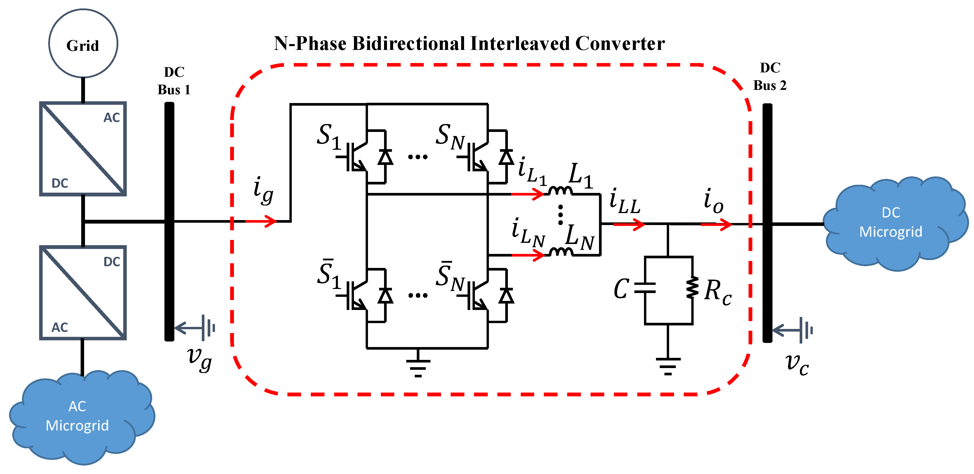
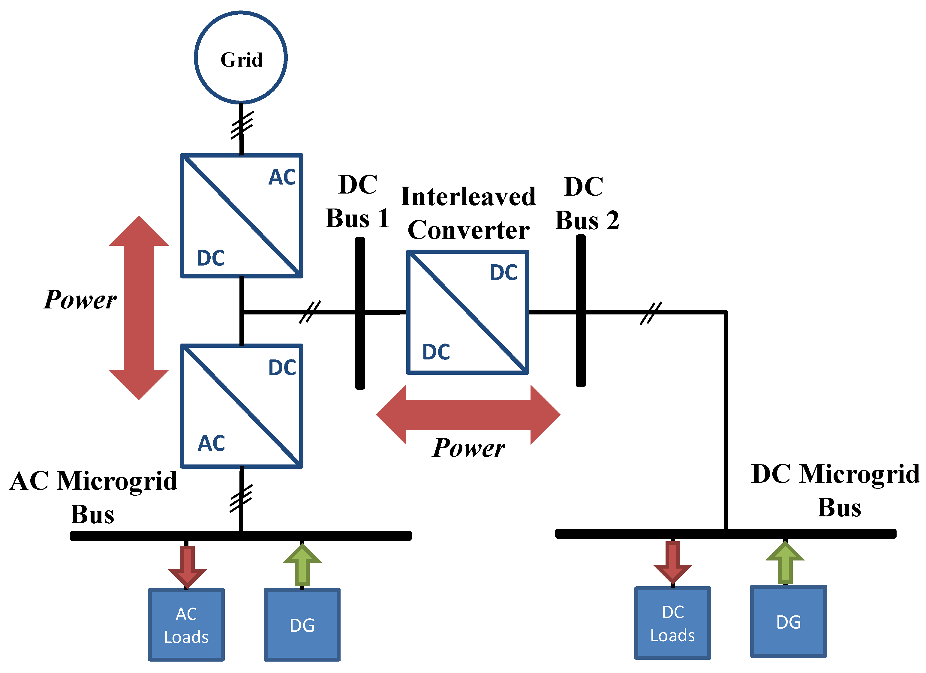
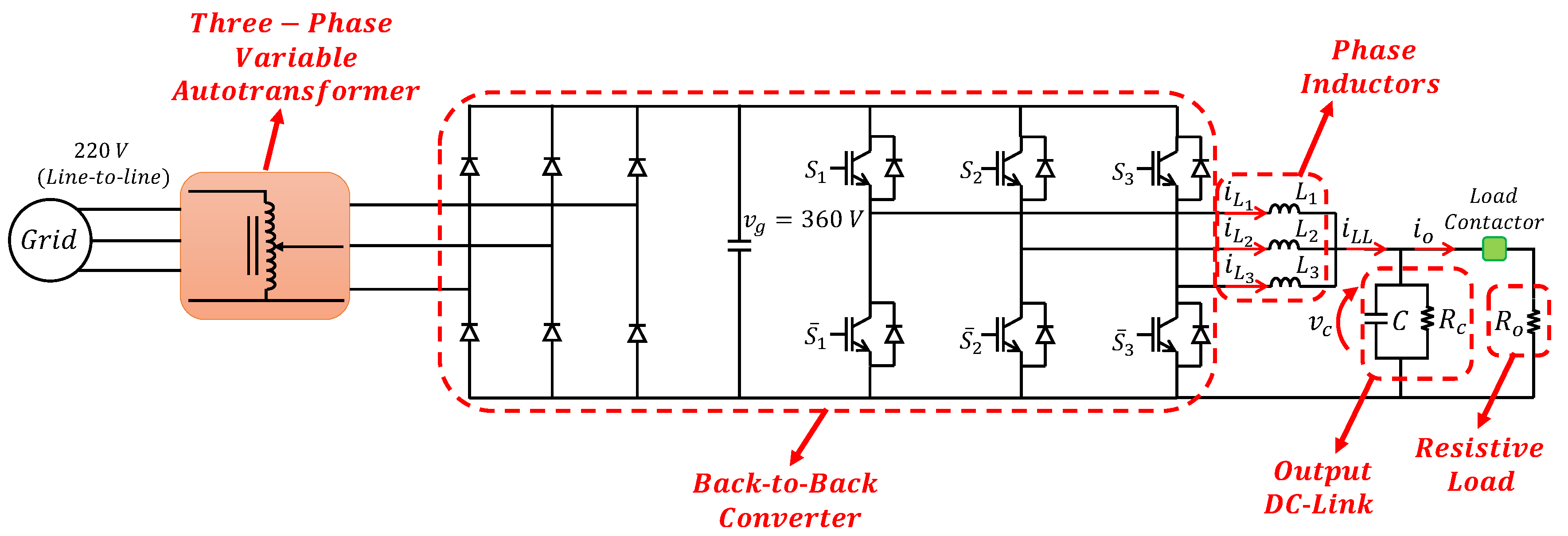
2. System Topology
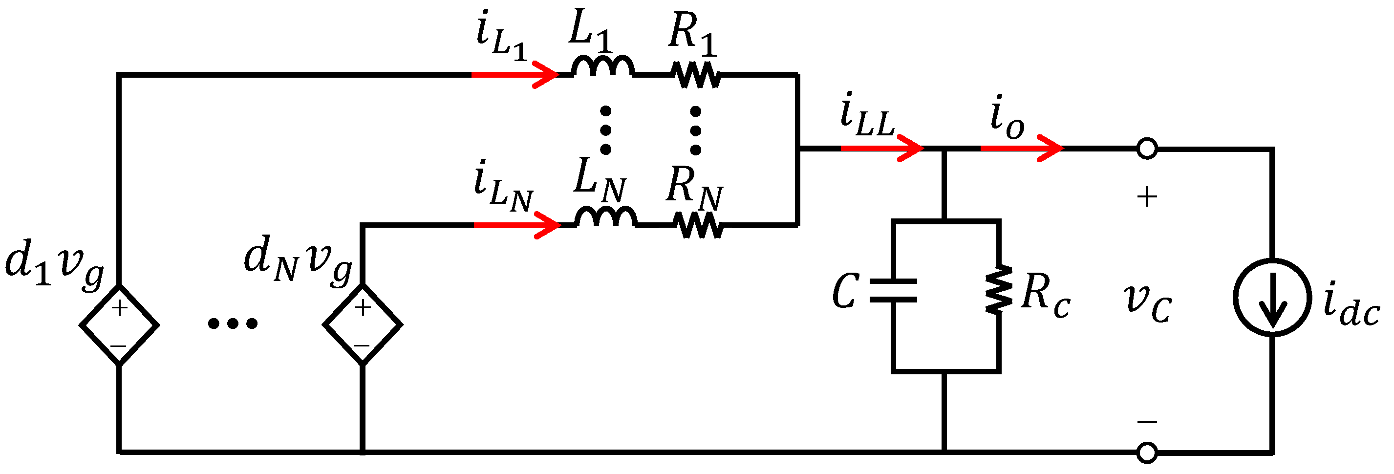
3. Interleaved Converter Modeling
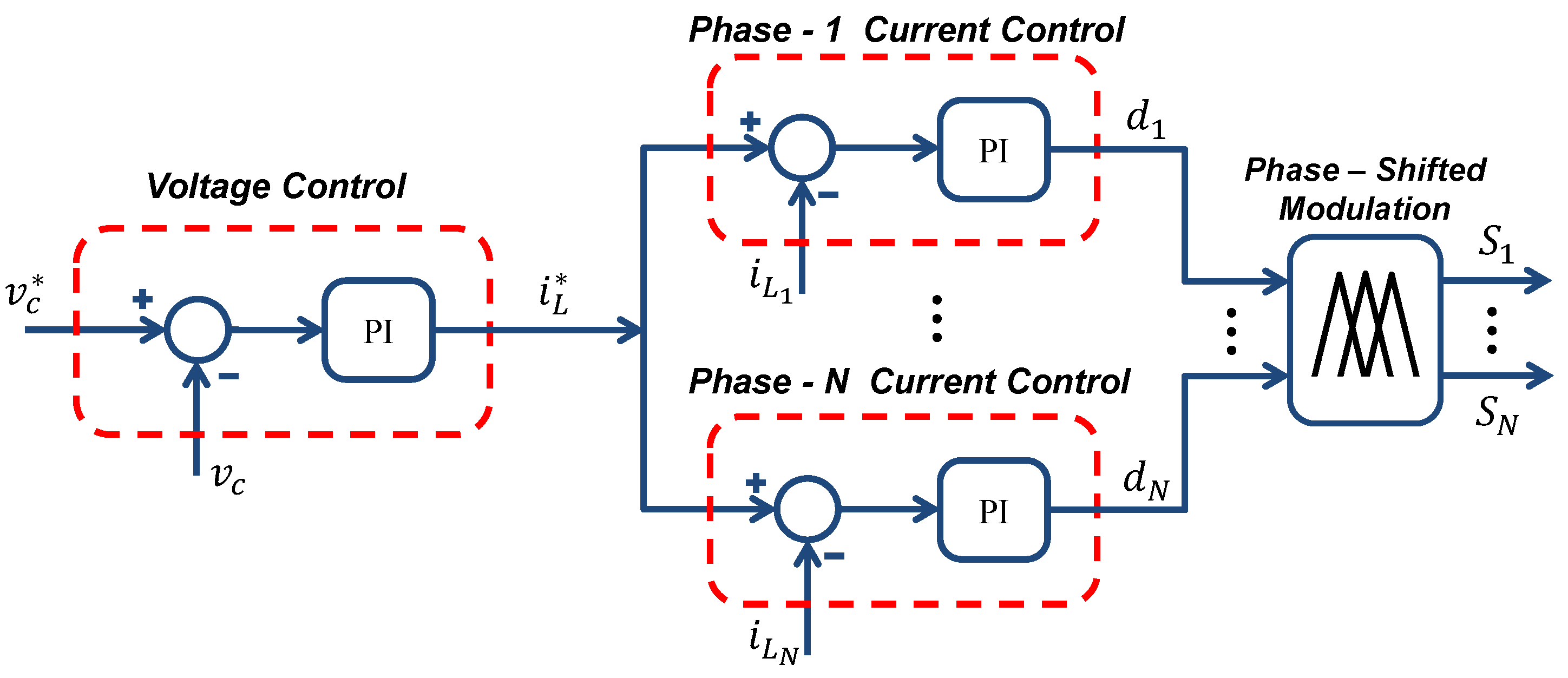
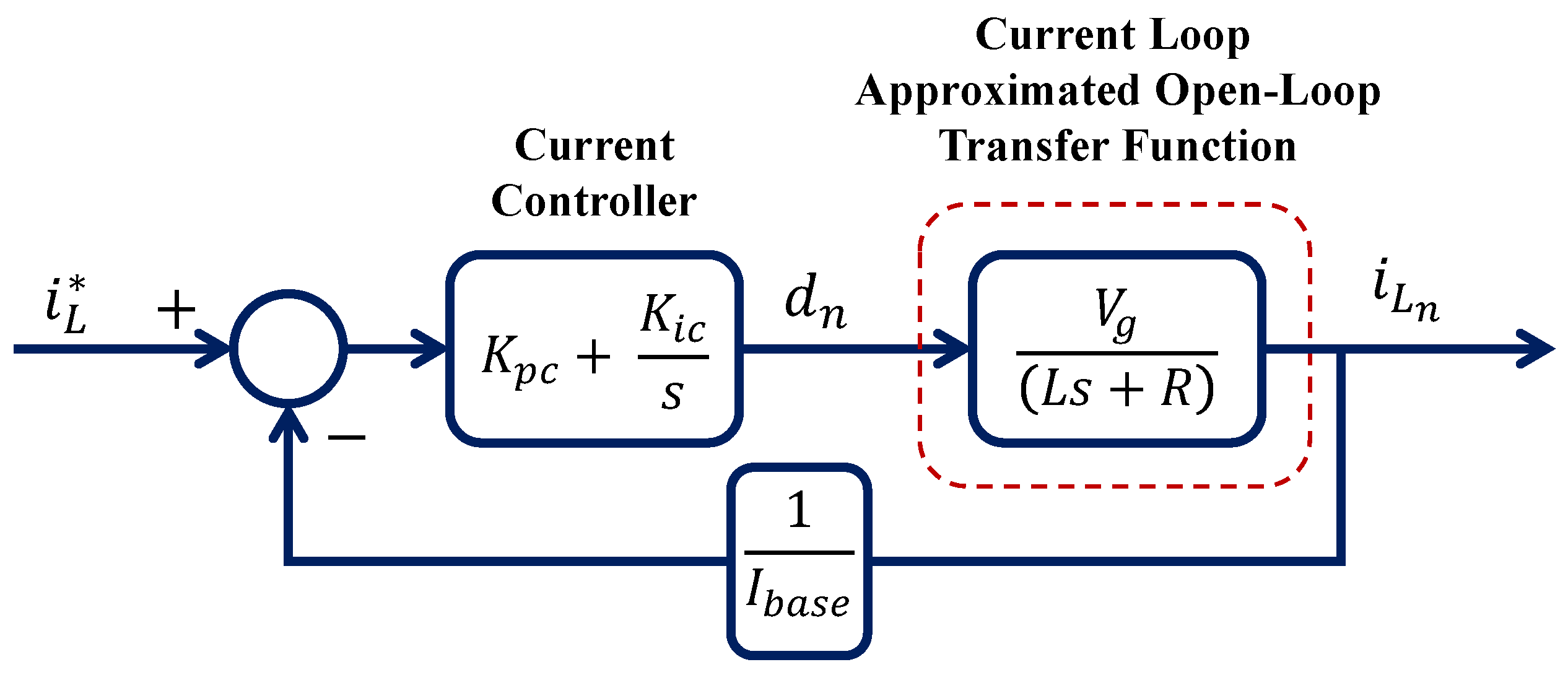
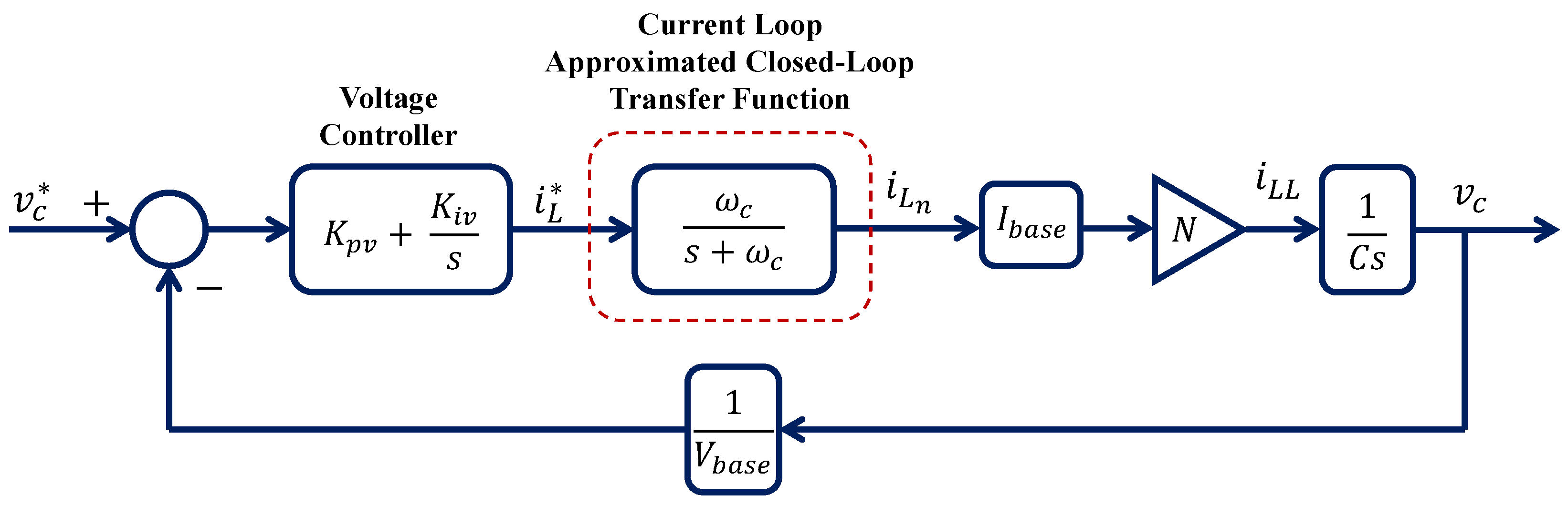
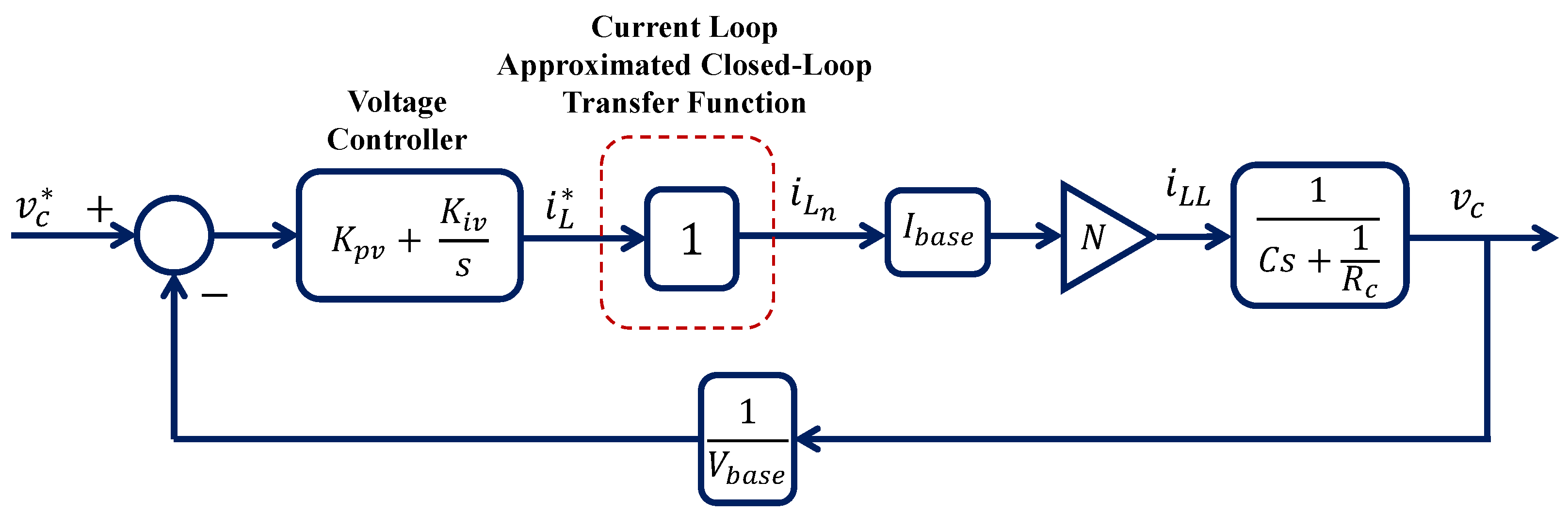
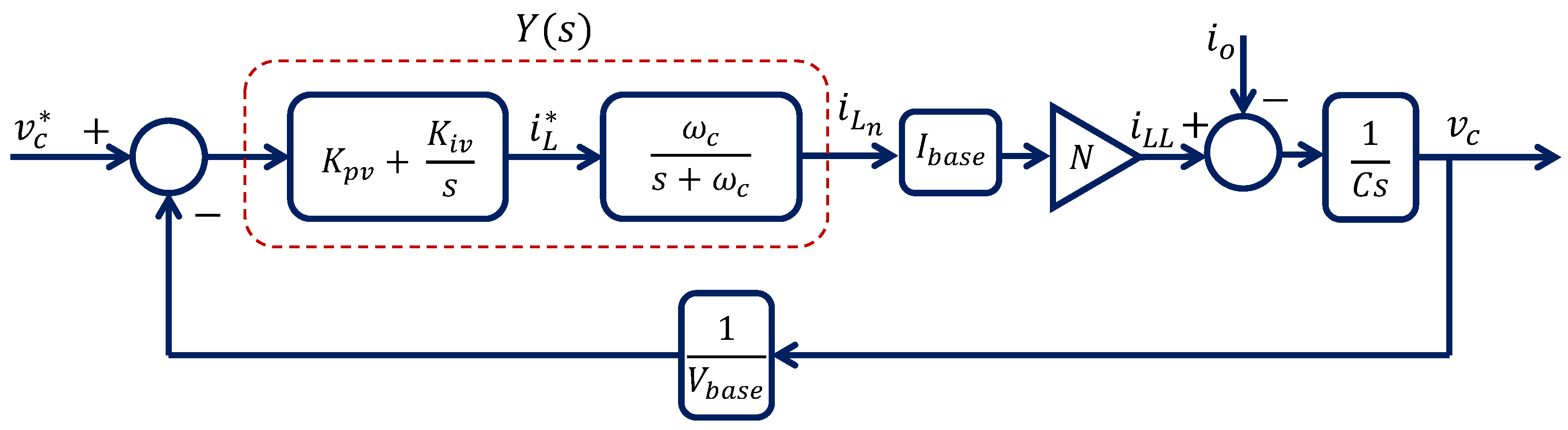
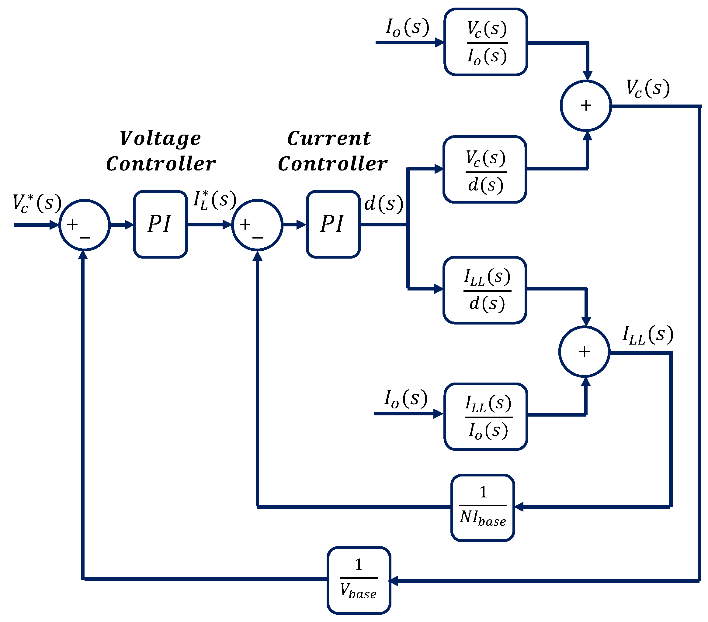
4. Control Design
4.1. Conventional Control Design
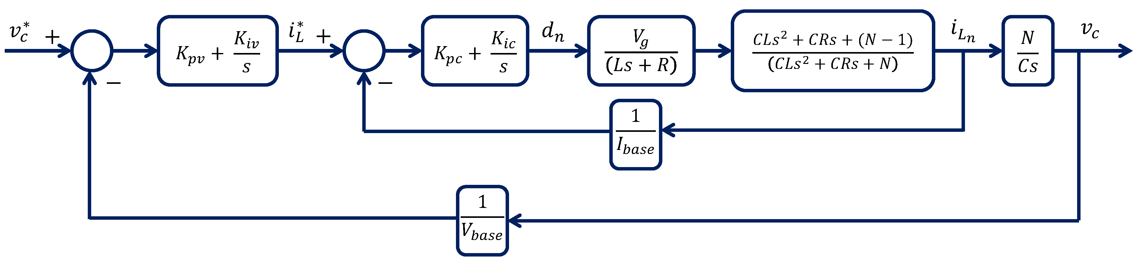
4.2. Proposed Control Design Method
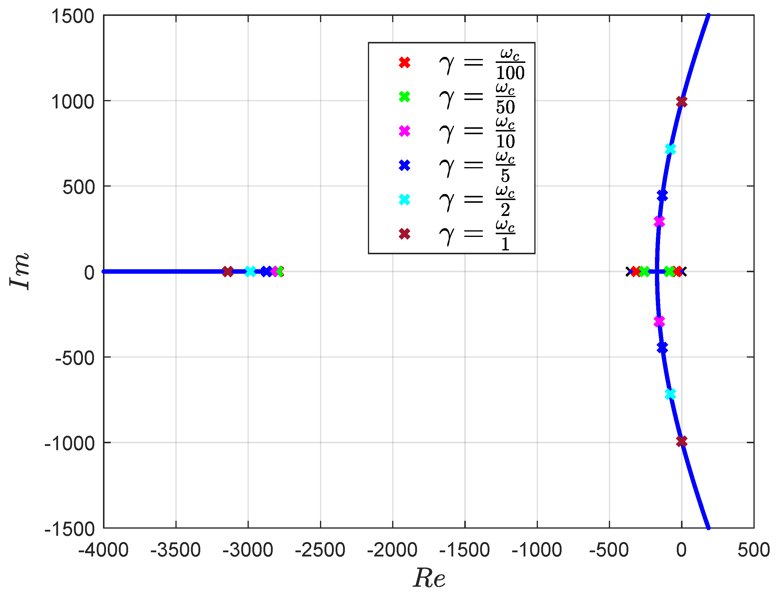
5. Stability Analysis
6. Simulation Results
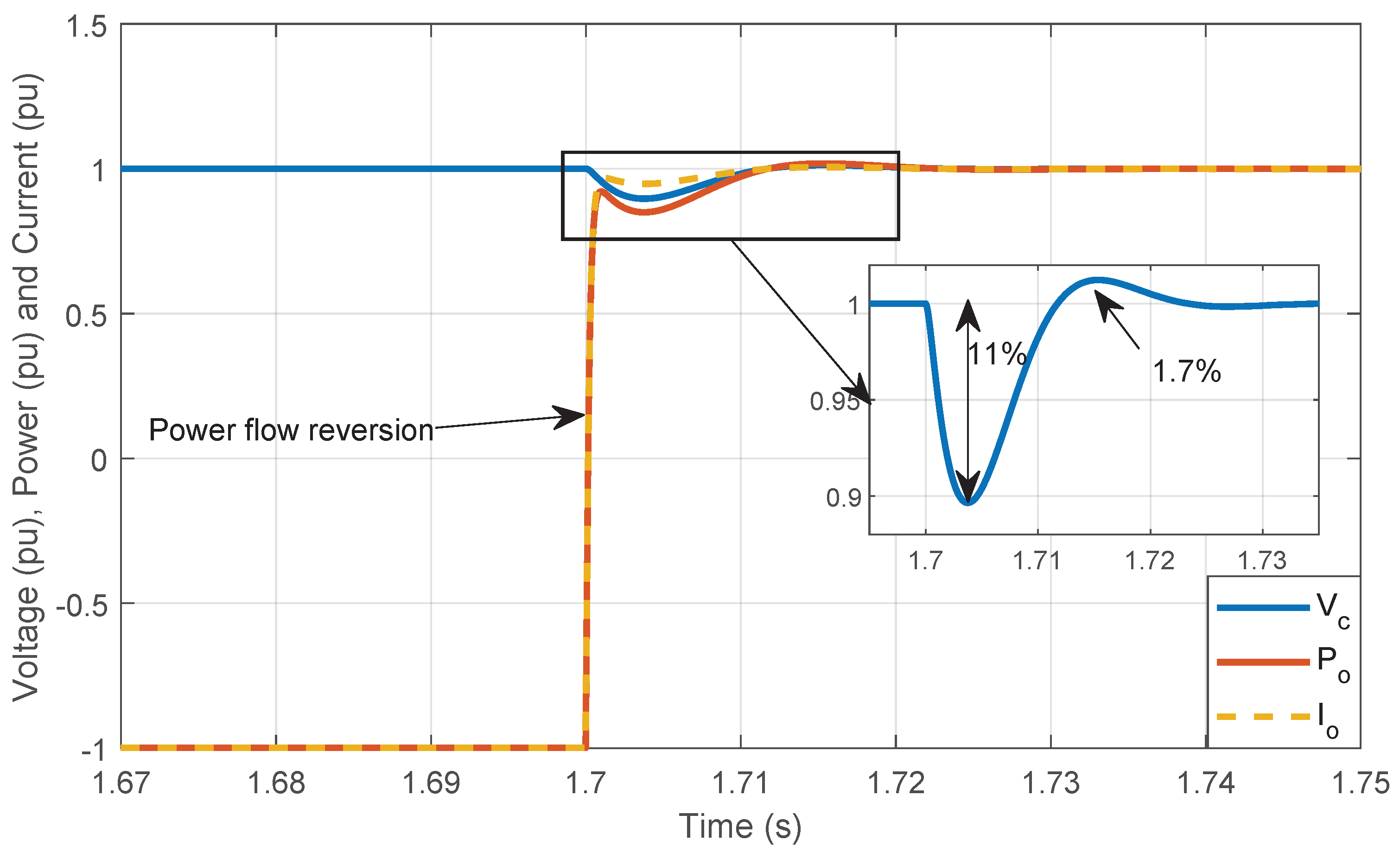
6.1. Hybrid Microgrid Operating with Bidirectional Power Flow
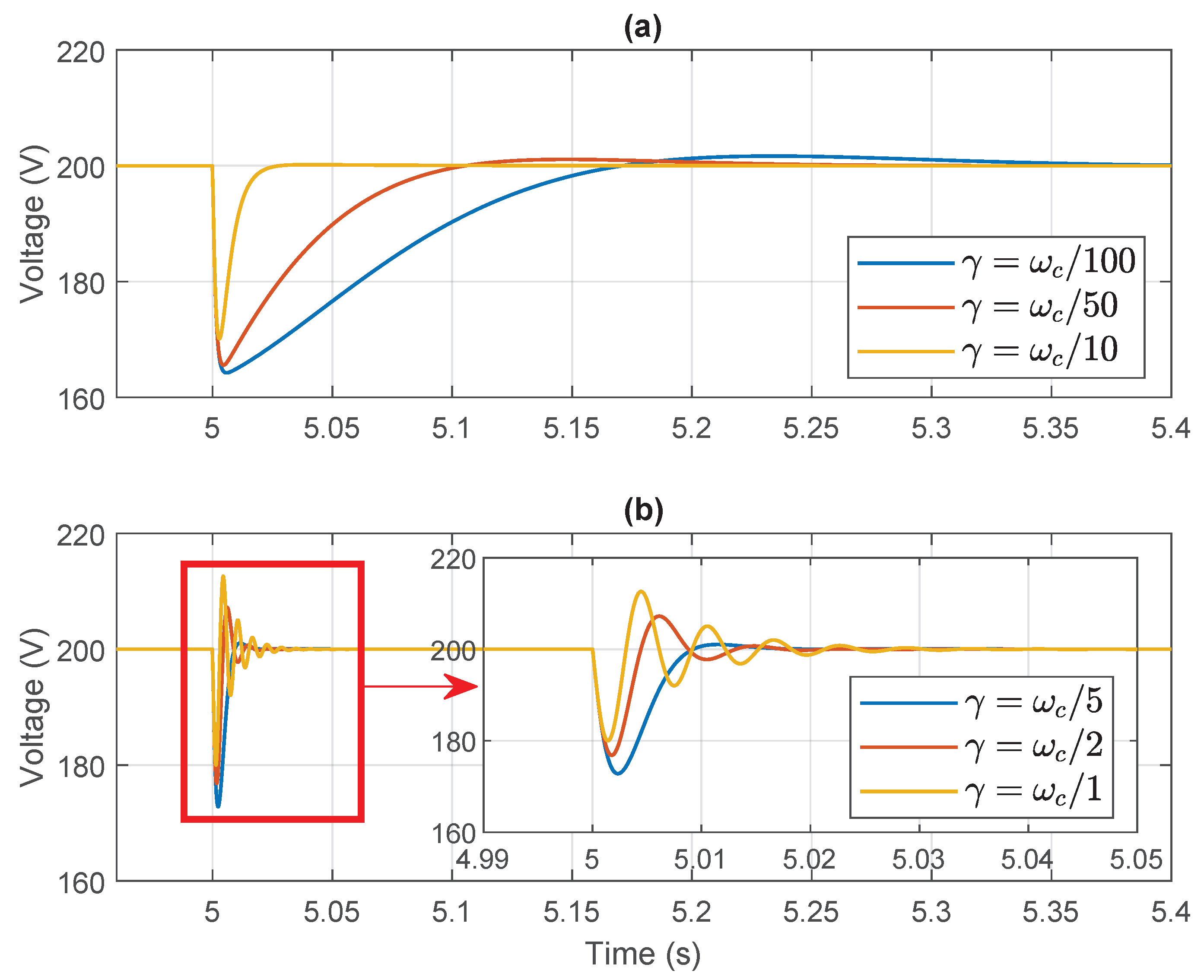
6.2. Evaluation of the Proposed Voltage Controller’s Design Technique in a Simulation Environment
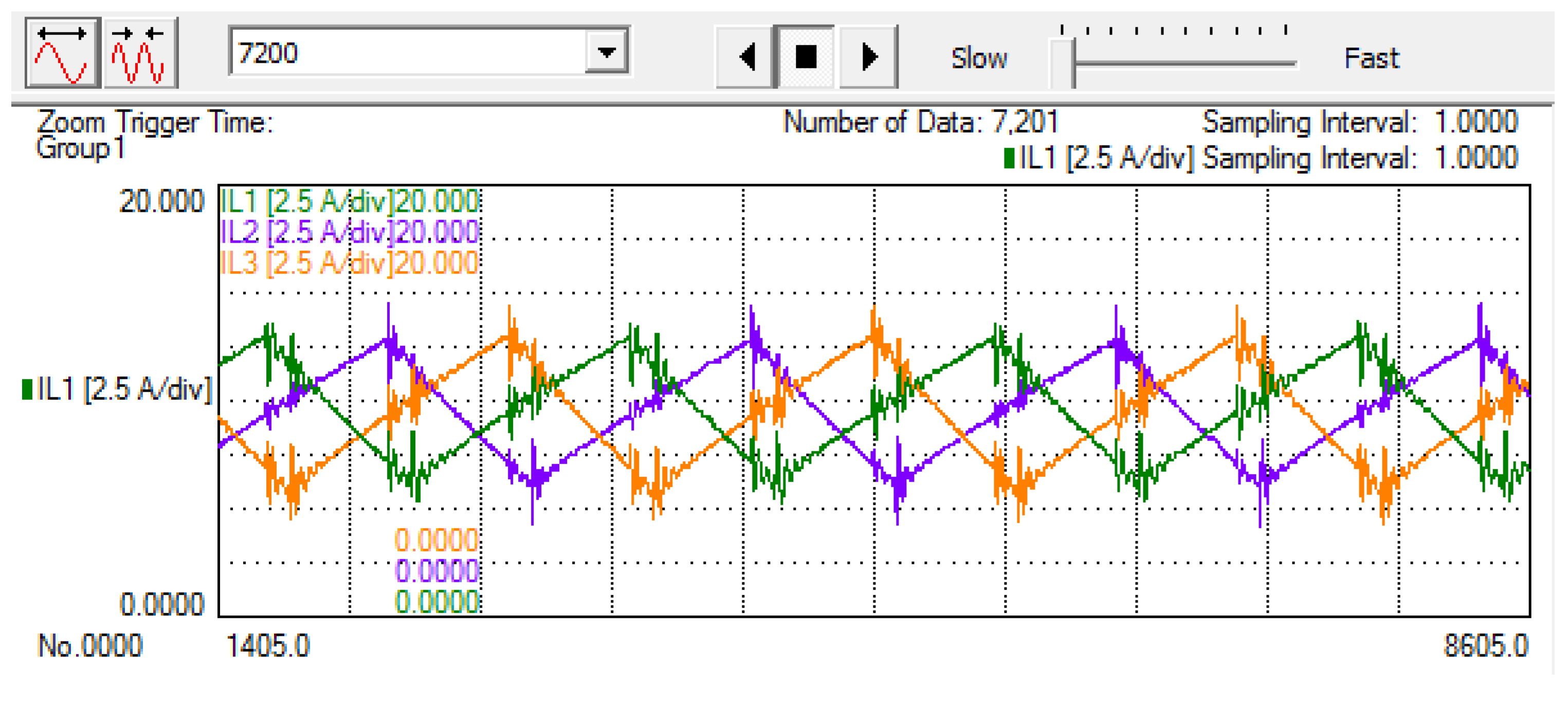
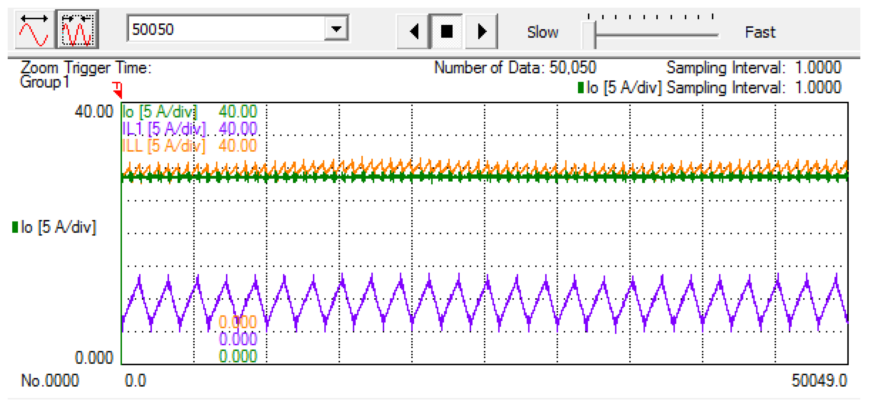
7. Experimental Results
7.1. Transient Operation Caused by Load Connection
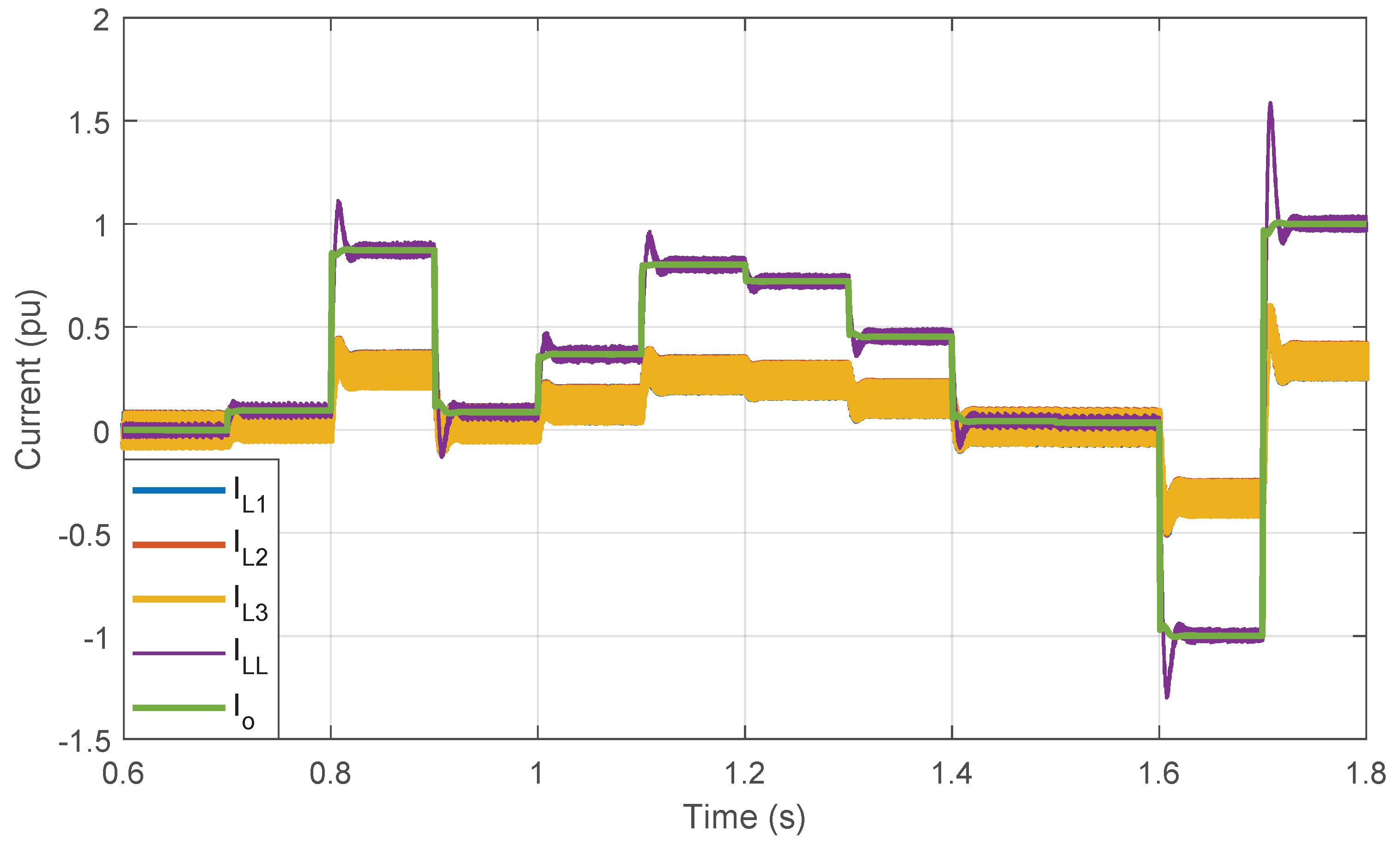
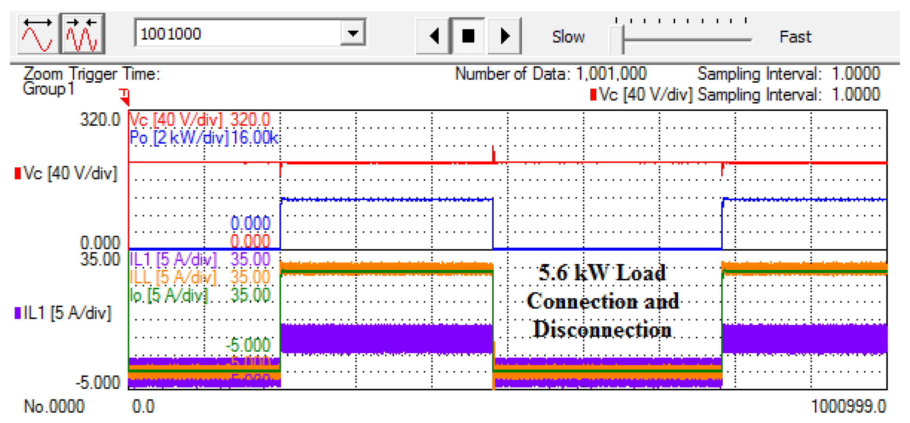
7.2. Microgrid Operation with Load Connection and Disconnection
7.3. Steady-State Operation
8. Conclusions
Author Contributions
Funding
Conflicts of Interest
References
- Parhizi, S.; Lotfi, H.; Khodaei, A.; Bahramirad, S. State of the art in research on microgrids: A review. IEEE Access 2015, 3, 890–925. [Google Scholar] [CrossRef]
- Wang, X.; Guerrero, J.M.; Blaabjerg, F.; Chen, Z. A Review of Power Electronics Based Microgrids. J. Power Electron. 2012, 12, 181–192. [Google Scholar] [CrossRef]
- Guerrero, J.M.; Chandorkar, M.; Lee, T.L.; Loh, P.C. Advanced Control Architectures for Intelligent Microgrids—Part I: Decentralized and Hierarchical Control. IEEE Trans. Ind. Electron. 2013, 60, 1254–1262. [Google Scholar] [CrossRef]
- Guerrero, J.M.; Loh, P.C.; Lee, T.L.; Chandorkar, M. Advanced Control Architectures for Intelligent Microgrids—Part II: Power Quality, Energy Storage, and AC/DC Microgrids. IEEE Trans. Ind. Electron. 2013, 60, 1263–1270. [Google Scholar] [CrossRef]
- Dragicevic, T.; Lu, X.; Vasquez, J.C.; Guerrero, J.M. DC Microgrids—Part I: A Review of Control Strategies and Stabilization Techniques. IEEE Trans. Power Electron. 2016, 31, 4876–4891. [Google Scholar] [CrossRef]
- Dragicevic, T.; Lu, X.; Vasquez, J.; Guerrero, J.M. DC Microgrids—Part II: A Review of Power Architectures, Applications, and Standardization Issues. IEEE Trans. Power Electron. 2016, 31, 3528–3549. [Google Scholar] [CrossRef]
- Che, L.; Shahidehpour, M. DC Microgrids: Economic Operation and Enhancement of Resilience by Hierarchical Control. IEEE Trans. Smart Grid 2014, 5, 2517–2526. [Google Scholar]
- Saeedifard, M.; Graovac, M.; Dias, R.F.; Iravani, R. DC Power Systems: Challenges and Opportunities. In Proceedings of the IEEE PES General Meeting, Providence, RI, USA, 25–29 July 2010; pp. 1–7. [Google Scholar]
- Liu, X.; Wang, P.; Loh, P.C. A Hybrid AC/DC Microgrid and Its Coordination Control. IEEE Trans. Smart Grid 2011, 2, 278–286. [Google Scholar]
- Majumder, R. A Hybrid Microgrid With DC Connection at Back to Back Converters. IEEE Trans. Smart Grid 2014, 5, 251–259. [Google Scholar] [CrossRef]
- Zhu, J.P.; Zhou, J.P.; Zhang, H. Research Progress of AC, DC and Their Hybrid Micro-grids. In Proceedings of the 2014 IEEE International Conference on System Science and Engineering (JCSSE), Shanghai, China, 11–13 July 2014. [Google Scholar]
- Syed, M.H.; Zeineldin, H.H.; El Moursi, M.S. Hybrid micro-grid operation characterisation based on stability and adherence to grid codes. IET Gener. Transm. Distrib. 2014, 8, 563–572. [Google Scholar] [CrossRef]
- Baumann, M.; Peters, J.; Weil, M.; Marcelino, C.; Almeida, P.; Wanner, E. Environmental Impacts of different Battery Technologies in Renewable Hybrid Micro-Grids. In Proceedings of the 2017 IEEE PES Innovative Smart Grid Technologies Conference Europe (ISGT-Europe), Torino, Italy, 26–29 September 2017. [Google Scholar]
- Hedel, K.K. High-Density Avionic Power Supply. IEEE Trans. Aerosp. Electron. Syst. 1980, AES-16, 615–619. [Google Scholar] [CrossRef]
- Shortt, D.J.; Michael, W.T.; Avant, R.L.; Palma, R.E. A 600 watt four stage phase-shifted-parallel DC-to-DC converter. In Proceedings of the 1985 IEEE Power Electronics Specialists Conference, Toulouse, France, 24–28 June 1985; pp. 136–143. [Google Scholar]
- Miwa, B.A.; Otten, D.M.; Schlecht, M.F. High efficiency power factor correction using interleaving techniques. In Proceedings of the 1992 Applied Power Electronics Conference and Exposition, APEC ’92, Boston, MA, USA, 23–27 February 1992. [Google Scholar]
- Chang, C.; Knights, M.A. Interleaving Technique in Distributed Power Conversion Systems. IEEE Trans. Circuits Syst. I Fundam. Theory Appl. 1995, 42, 245–251. [Google Scholar] [CrossRef]
- Chang, C. Current Ripple Bounds in Interleaved DC–DC Power Converters. In Proceedings of the 1995 International Conference on Power Electronics and Drive Systems, PEDS 95, Singapore, 21–24 February 1995; Volume 2, pp. 738–743. [Google Scholar]
- Balogh, L.; Redl, R. Power-Factor Correction with Interleaved Boost Converters in Continuous-Inductor- Current Mode. In Proceedings of the Eighth Annual Applied Power Electronics Conference and Exposition, San Diego, CA, USA, 7–11 March 1993; pp. 168–174. [Google Scholar]
- Chandrasekaran, S.; Gokdere, L.U. Integrated Magnetics for Interleaved DC–DC Boost Converter for Fuel Cell Powered Vehicles. In Proceedings of the 2004 35th Annual IEEE Power Electronics Specialisls Conference, Aachen, Germany, 20–25 June 2004; pp. 356–361. [Google Scholar]
- Hirakawa, M.; Watanabe, Y.; Nagano, M.; Andoh, K.; Nakatomi, S.; Hashino, S.; Shimizu, T. High Power DC / DC Converter using Extreme Close-Coupled Inductors aimed for Electric Vehicles. In Proceedings of the 2010 International Power Electronics Conference—ECCE ASIA, Sapporo, Japan, 21–24 June 2010; pp. 2941–2948. [Google Scholar]
- Hirakawa, M.; Nagano, M.; Watanabe, Y.; Ando, K.; Nakatomi, S.; Hashino, S. High Power Density Interleaved DC/DC Converter using a 3-phase Integrated Close-Coupled Inductor Set aimed for Electric Vehicles. In Proceedings of the 2010 IEEE Energy Conversion Congress and Exposition, Atlanta, GA, USA, 12–16 September 2010. [Google Scholar]
- Schroeder, J.C.; Wittig, B.; Fuchs, F.W. High Efficient Battery Backup System for Lift Trucks Using Interleaved-Converter and Increased EDLC Voltage Range. In Proceedings of the IECON 2010—36th Annual Conference on IEEE Industrial Electronics Society, Glendale, AZ, USA, 7–10 November 2010; pp. 2334–2339. [Google Scholar]
- Ni, L.; Patterson, D.J.; Hudgins, J.L. High Power Current Sensorless Bidirectional 16-Phase Interleaved DC–DC Converter for Hybrid Vehicle Application. IEEE Trans. Power Electron. 2012, 27, 1141–1151. [Google Scholar] [CrossRef]
- Hegazy, O.; Mierlo, J.V.; Lataire, P. Analysis, Modeling, and Implementation of a Multidevice Interleaved DC/DC Converter for Fuel Cell Hybrid Electric Vehicles. IEEE Trans. Power Electron. 2012, 27, 4445–4458. [Google Scholar] [CrossRef]
- Schroeder, J.C.; Petersen, M.; Fuchs, F.W. One-Sensor Current Sharing in Multiphase Interleaved DC/DC Converters with Coupled Inductors. In Proceedings of the 15th International Power Electronics and Motion Control Conference, EPE-PEMC 2012 ECCE Europe, Novi Sad, Serbia, 4–6 September 2012; pp. 1–7. [Google Scholar]
- Lu, S.; Mu, M.; Jiao, Y.; Lee, F.C.; Zhao, Z. Coupled inductors in interleaved multiphase three- level DC–DC Converter for High Power Energy Storage Applications. In Proceedings of the 2014 IEEE Conference and Expo Transportation Electrification Asia-Pacific (ITEC Asia-Pacific), Beijing, China, 31 August–3 September 2014; pp. 1–6. [Google Scholar]
- Magne, P.; Liu, P.; Bilgin, B.; Emadi, A. Investigation of Impaet of Number of Phases in Interleaved dc-dc Boost Converter. In Proceedings of the 2015 IEEE Transportation Electri cation Conference and Expo (ITEC), Dearborn, MI, USA, 14–17 June 2015. [Google Scholar]
- Jung, M.; Lempidis, G.; Hölsch, D.; Steffen, J. Optimization considerations for Interleaved DC–DC Converters for EV Battery charging applications, in terms of partial load efficiency and power density. In Proceedings of the 2015 17th European Conference on Power Electronics and Applications (EPE’15 ECCEEurope), Geneva, Switzerland, 8–10 September 2015. [Google Scholar]
- Schumacher, D.; Magne, P.; Preindl, M.; Bilgin, B.; Emadi, A. Closed Loop Control of a Six Phase Interleaved Bidirectional dc-dc Boost Converter for an EV/ HEV Application. In Proceedings of the 2016 IEEE Transportation Electri cation Conference and Expo (ITEC), Dearborn, MI, USA, 26–29 June 2016. [Google Scholar]
- Karimi, R.; Kaczorowski, D.; Zlotnik, A.; Mertens, A. Loss Optimizing Control of a Multiphase Interleaving DC–DC Converter for Use in a Hybrid Electric Vehicle Drivetrain. In Proceedings of the 2016 IEEE Energy Conversion Congress and Exposition (ECCE), Milwaukee, WI, USA, 18–22 September 2016. [Google Scholar]
- Melo, R.R.; Antunes, F.L.M.; Daher, S. Bidirectional interleaved dc-dc converter for supercapacitor-based energy storage systems applied to microgrids and electric vehicles. In Proceedings of the 2014 16th European Conference on Power Electronics and Applications, Lappeenranta, Finland, 26–28 August 2014. [Google Scholar]
- Chaitanya, N.; Anjaneyulu, K.S.R.; Sekhar, K.C. Performance Analysis of a Hybrid Power System with Three Phase Interleaved Bidirectional Converter. In Proceedings of the 2014 International Conference on Smart Electric Grid (ISEG), Guntur, India, 19–20 September 2014; pp. 1–8. [Google Scholar]
- Correa-Betanzo, C.; Calleja, H.; Morales-Morales, C.; López-Zapata, B. An Interleaved Single Phase Grid Tied Converter aimed at DC Microgrid Applications. In Proceedings of the 2016 13th International Conference on Power Electronics (CIEP) An, Guanajuato, Mexico, 20–23 June 2016; pp. 277–282. [Google Scholar]
- Krishna, D.S.G.; Patra, M. Modeling of Multi-Phase DC–DC Converter with A Compensator for Better Voltage Regulation in DC Micro-grid Application. In Proceedings of the International Conference on Signal Processing, Communication, Power and Embedded System (SCOPES)—2016 Modeling, Odisha, India, 3–4 October 2016; pp. 989–994. [Google Scholar]
- Kan, Z. Interleaved Three-Level Bi-directional DC–DC Converter and Power Flow Control. In Proceedings of the 2018 3rd International Conference on Intelligent Green Building and Smart Grid (IGBSG), Yilan, Taiwan, 22–25 April 2018; pp. 1–4. [Google Scholar]
- Tricarico, T.; Soares, M.; Gontijo, G.; Oliveira, D.; Dicler, F.; Aredes, M. Design, Control and Stability Analysis of an Interleaved DC Converter for Voltage Interfacing Application in Microgrids. In Proceedings of the XXII Brazilian Conference on Automation (CBA 2018), João Pessoa, Brazil, 9–12 September 2018. [Google Scholar]
- Gao, Z. Scaling and Bandwidth-Parameterization Based Controller Tuning. In Proceedings of the 2003 American Control Conference, Denver, CO, USA, 4–6 June 2003; pp. 4989–4996. [Google Scholar]


| Parameter | Value |
|---|---|
| N | 3 |
| 980 V | |
| 450 V | |
| L | 2.5 mH |
| C | 9.3 μF |
| R | 0.0 Ω |
| 450 V | |
| 124 A | |
| 56 kW | |
| rad/s | |
| rad/s | |
| Parameter | Value |
|---|---|
| N | 3 |
| 360 V | |
| L | 2.5 mH |
| C | 1.175 mF |
| R | 0.0 Ω |
| 200 V | |
| 28 A | |
| rad/s | |
| rad/s |
| Component | Value |
|---|---|
| 2.5 mH | |
| C | 1.175 mF |
| 47.0 kΩ | |
| 7.5 Ω |
© 2019 by the authors. Licensee MDPI, Basel, Switzerland. This article is an open access article distributed under the terms and conditions of the Creative Commons Attribution (CC BY) license (http://creativecommons.org/licenses/by/4.0/).
Share and Cite
Tricarico, T.; Gontijo, G.; Neves, M.; Soares, M.; Aredes, M.; Guerrero, J.M. Control Design, Stability Analysis and Experimental Validation of New Application of an Interleaved Converter Operating as a Power Interface in Hybrid Microgrids. Energies 2019, 12, 437. https://doi.org/10.3390/en12030437
Tricarico T, Gontijo G, Neves M, Soares M, Aredes M, Guerrero JM. Control Design, Stability Analysis and Experimental Validation of New Application of an Interleaved Converter Operating as a Power Interface in Hybrid Microgrids. Energies. 2019; 12(3):437. https://doi.org/10.3390/en12030437
Chicago/Turabian StyleTricarico, Thiago, Gustavo Gontijo, Marcello Neves, Matheus Soares, Mauricio Aredes, and Josep M. Guerrero. 2019. "Control Design, Stability Analysis and Experimental Validation of New Application of an Interleaved Converter Operating as a Power Interface in Hybrid Microgrids" Energies 12, no. 3: 437. https://doi.org/10.3390/en12030437
APA StyleTricarico, T., Gontijo, G., Neves, M., Soares, M., Aredes, M., & Guerrero, J. M. (2019). Control Design, Stability Analysis and Experimental Validation of New Application of an Interleaved Converter Operating as a Power Interface in Hybrid Microgrids. Energies, 12(3), 437. https://doi.org/10.3390/en12030437