Analysis and Design of High-Efficiency Bidirectional GaN-Based CLLC Resonant Converter

Abstract
: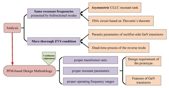
1. Introduction
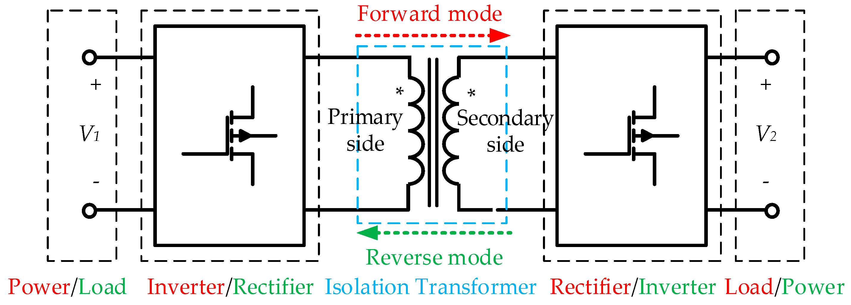
2. Analysis of Bidirectional CLLC Resonant Converter
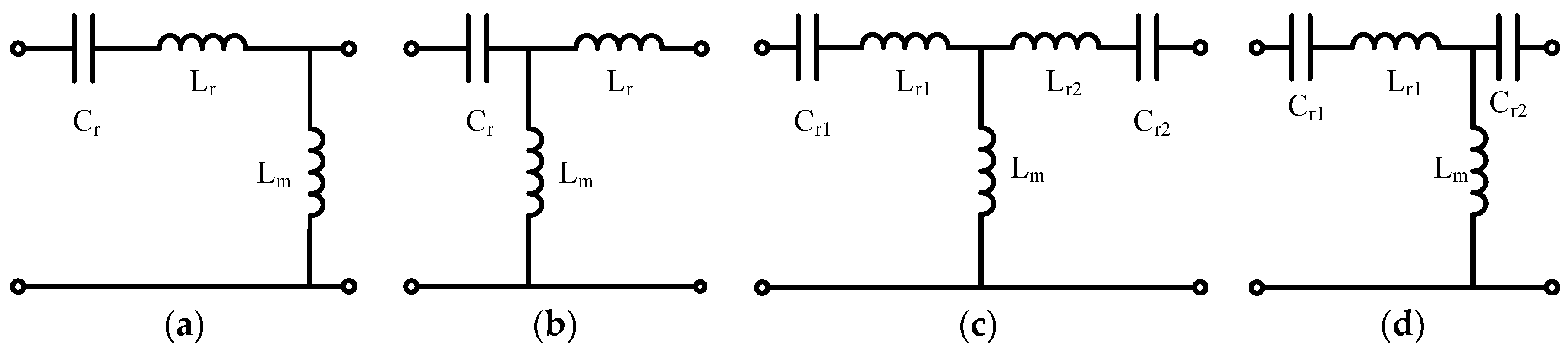
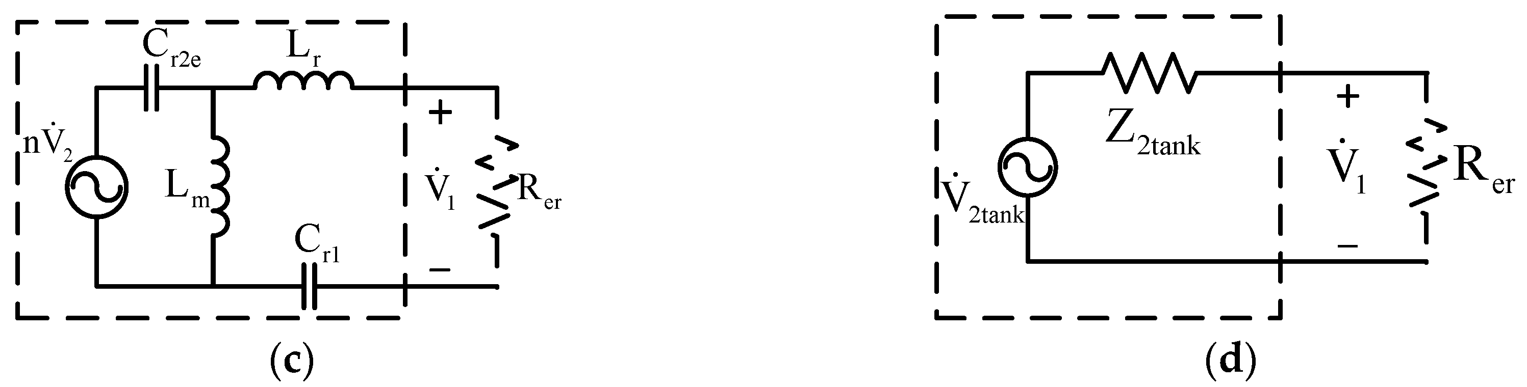
2.1. Resonant Frequencies of Bidirectional CLLC Resonant Converter
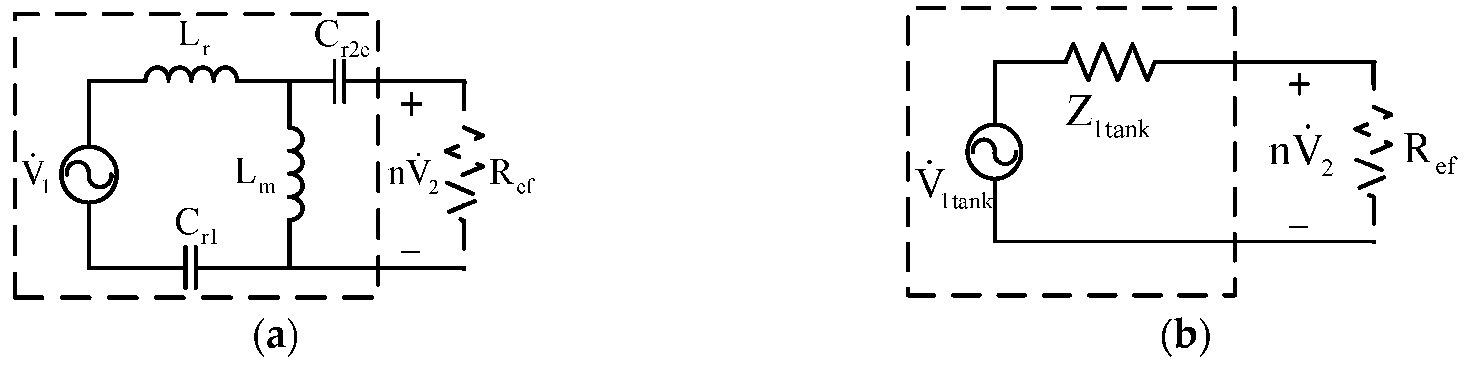
2.2. Auxiliary Parameters
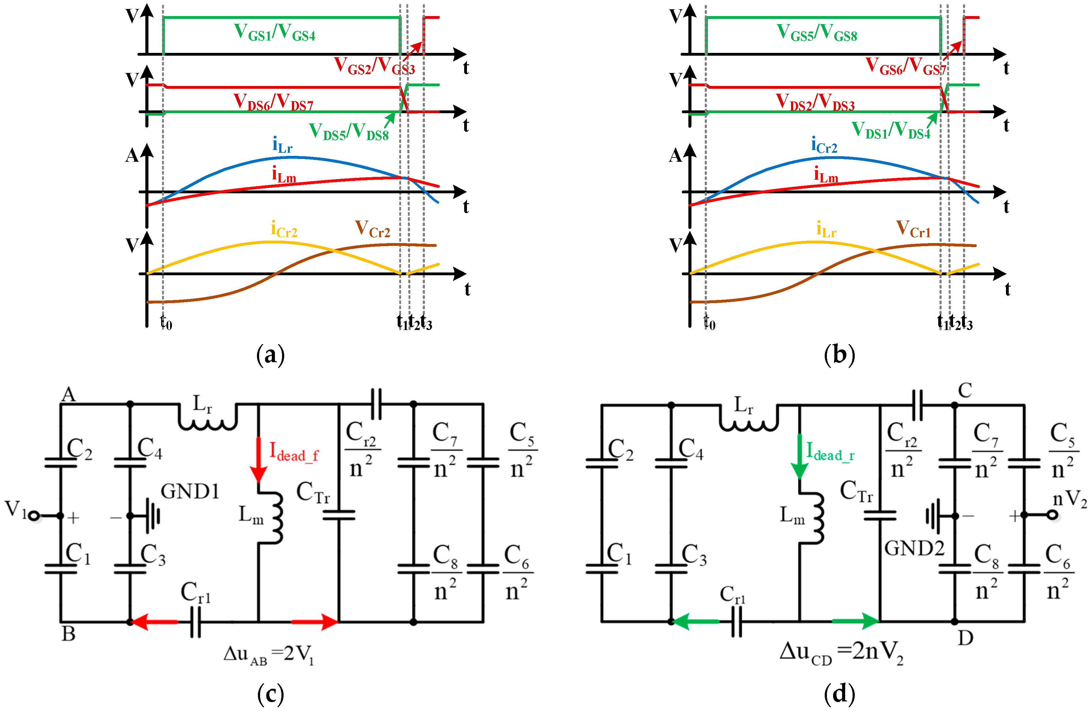
2.3. Improved Zero-Voltage Switching Condition for Bidirectional CLLC Resonant Converter
- The operating frequency is very close to the resonant frequency aiming for optimal operation, with continuous current in the inverter side;
- The process of charging and discharging parasitic capacitance is extremely short with constant inverter-side current taken into account.
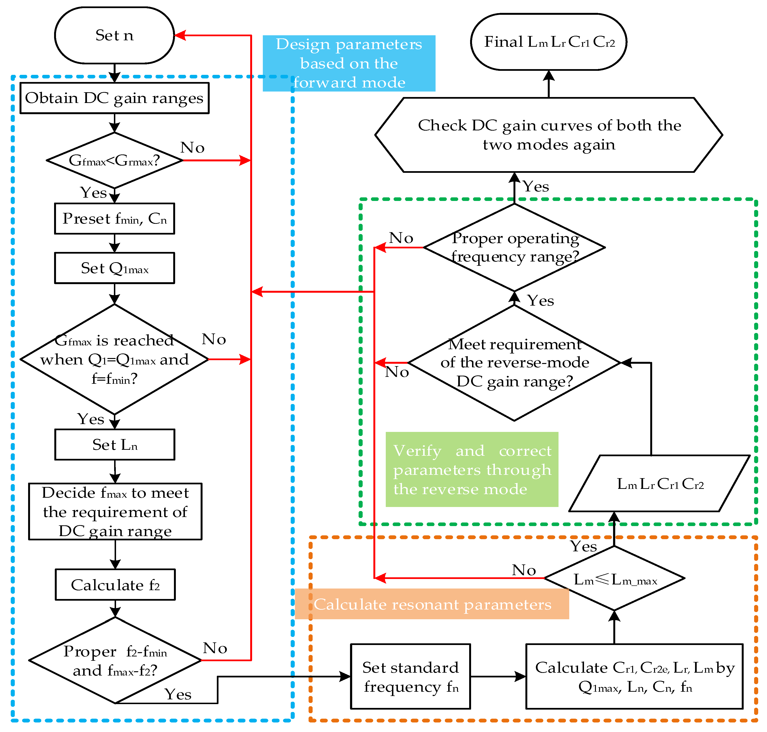
3. Design Methodology of GaN-Based Bidirectional CLLC Resonant Converter
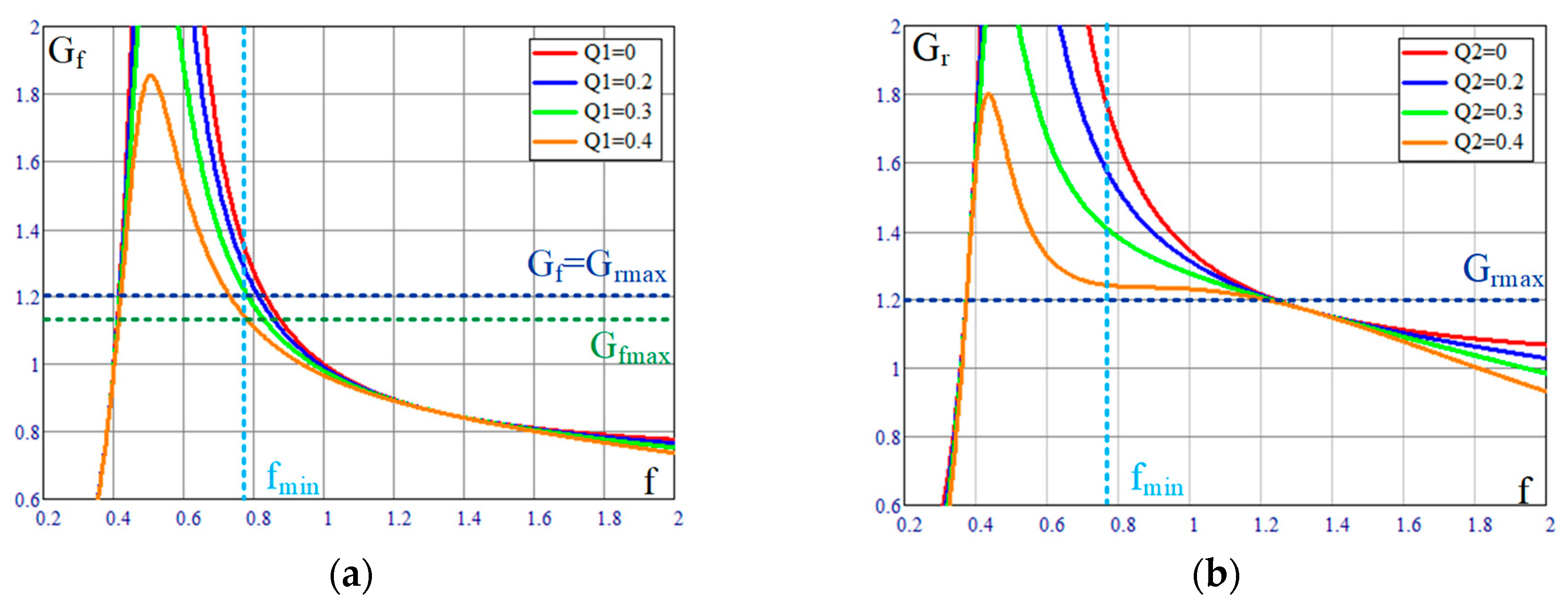
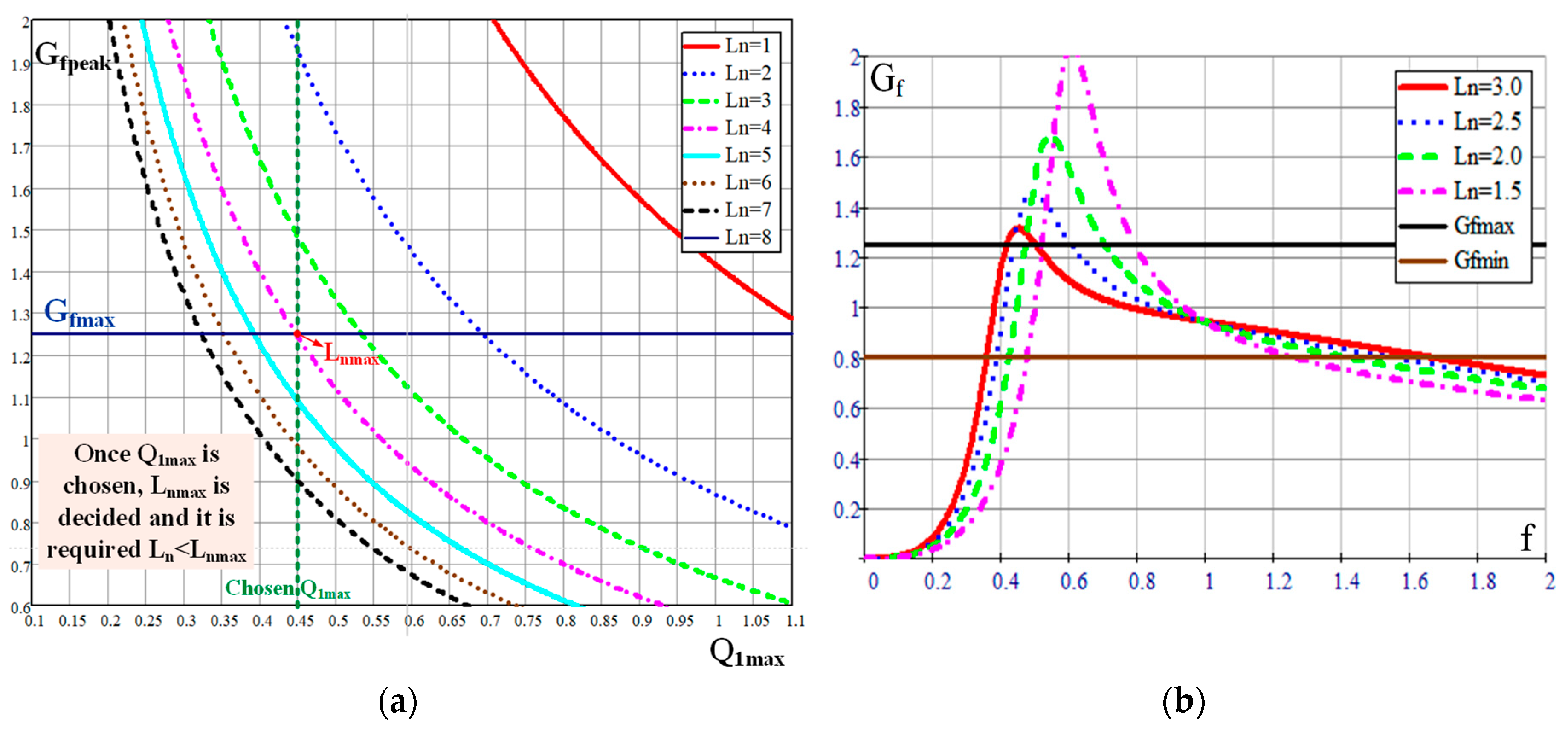
3.1. Design Procedures
3.2. Parameters of the Prototype
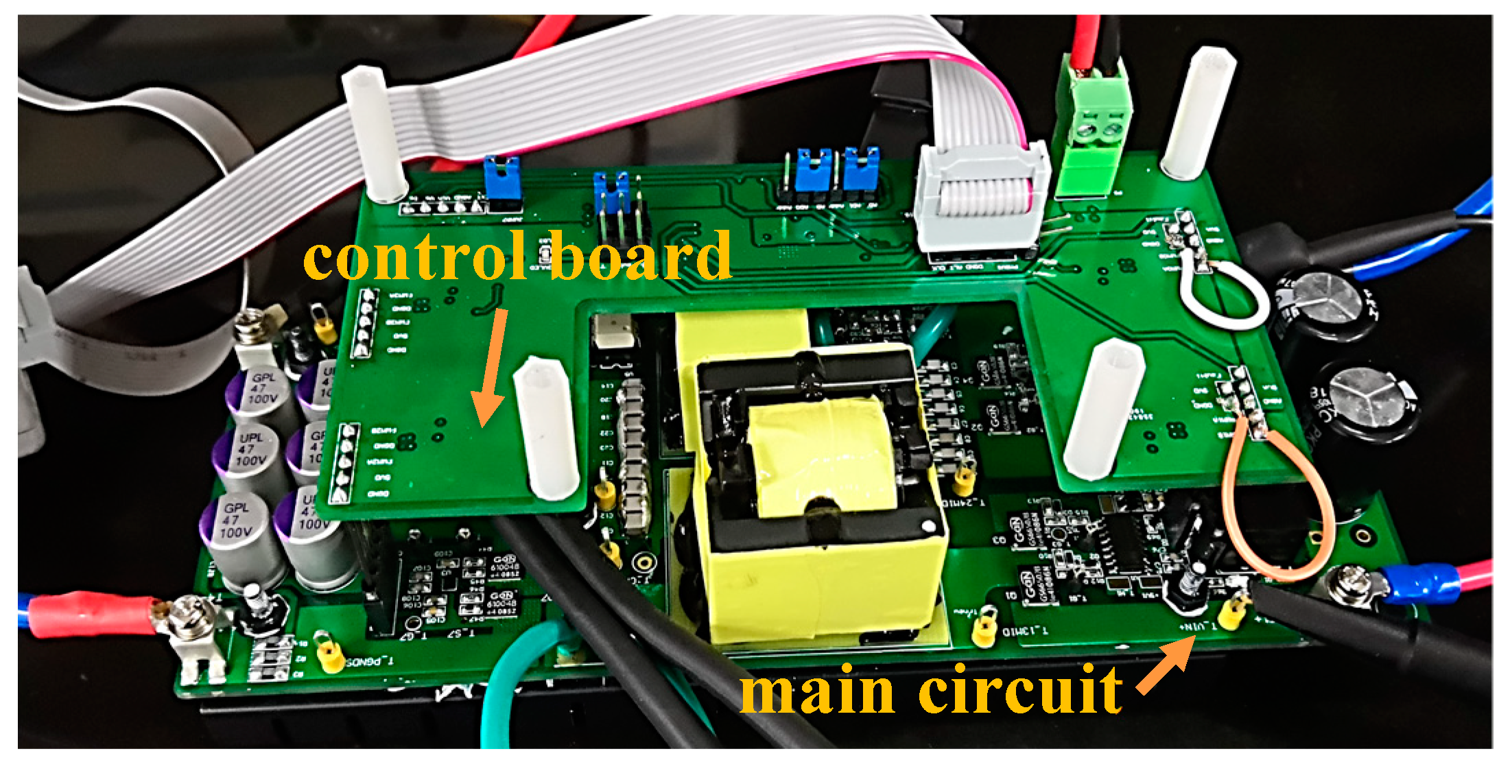
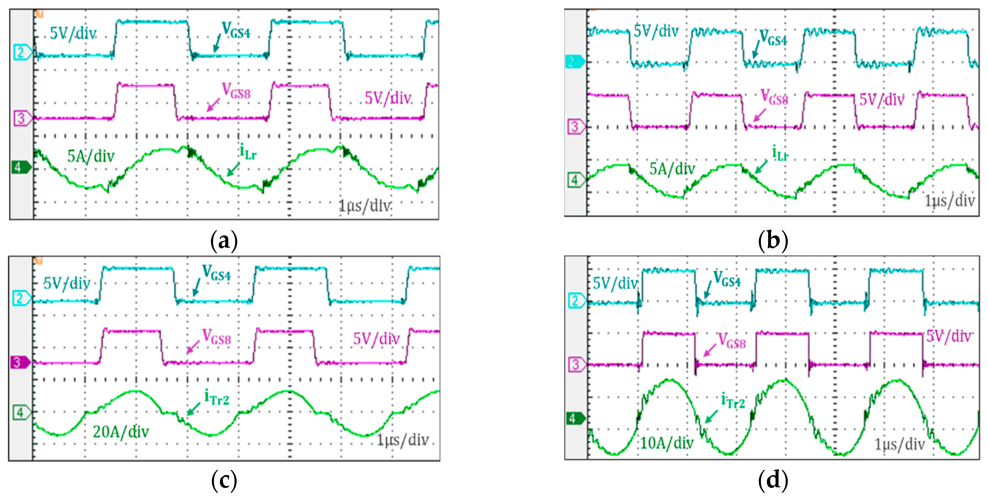
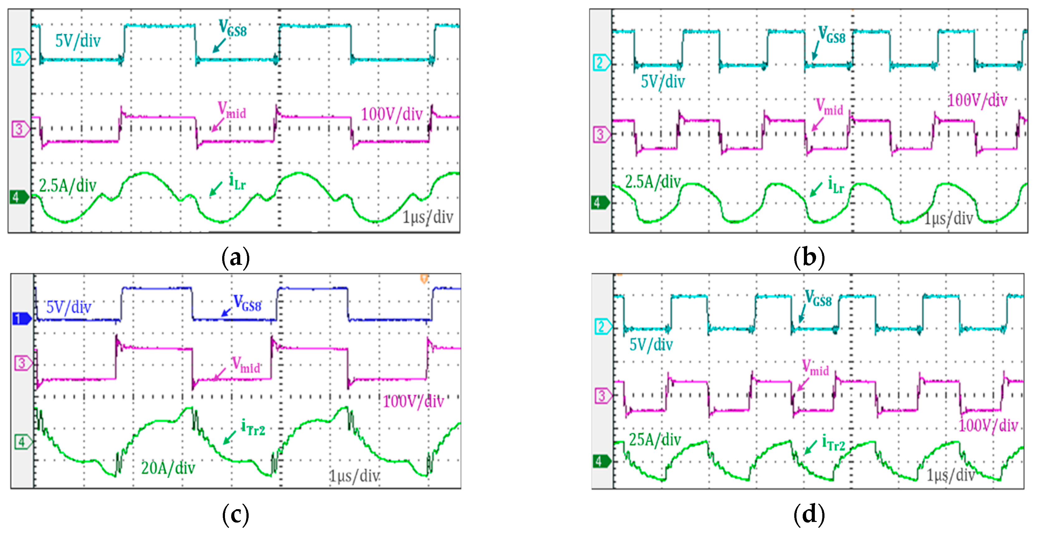
4. Experimental Verification
5. Conclusions
Author Contributions
Funding
Conflicts of Interest
References
- Wu, M.; Flynn, D.; Szymczak, A. Design and implementation of ZVZCS in full bridge DC/DC converter with digital control in arc welding machines application. In Proceedings of the IEEE International Symposium on Industrial Electronics, Edinburgh, UK, 19–21 June 2017. [Google Scholar]
- Kato, H.; Matsuo, H.; Ito, T.; Kawazu, S.; Kawahara, D.; Motomura, S.; Hamaguchie, R. Comparative analysis of full bridge and half bridge current resonant DC-DC converter. In Proceedings of the 33rd International Telecommunications Energy Conference (INTELEC), Amsterdam, The Netherlands, 9–13 October 2011. [Google Scholar]
- Kundu, U.; Yenduri, K.; Sensarma, P. Accurate ZVS Analysis for Magnetic Design and Efficiency Improvement of Full-Bridge LLC Resonant Converter. IEEE Trans. Power Electron. 2016, 32, 1703–1706. [Google Scholar] [CrossRef]
- Joung, M.; Kim, H.; Baek, J. Dynamic analysis and optimal design of high efficiency full bridge LLC resonant converter for server power system. In Proceedings of the Applied Power Electronics Conference and Exposition, Orlando, FL, USA, 5–9 February 2013. [Google Scholar]
- Severns, R.P. Topologies for three-element resonant converters. IEEE Trans. Power Electron. 1992, 7, 89–98. [Google Scholar] [CrossRef]
- Jung, J.H.; Kim, H.S.; Ryu, M.H.; Baek, J.W. Design Methodology of Bidirectional CLLC Resonant Converter for High-Frequency Isolation of DC Distribution Systems. IEEE Trans. Power Electron. 2013, 28, 1741–1755. [Google Scholar] [CrossRef]
- Dalala, Z.M.; Zahid, Z.U.; Saadeh, O.S.; Lai, J.S. Modeling and Controller Design of a Bidirectional Resonant Converter Battery Charger. IEEE Access 2018, 6, 23338–23350. [Google Scholar] [CrossRef]
- Jung, J.H.; Kim, H.S.; Kim, J.H.; Ryu, M.H.; Baek, J.W. High efficiency bidirectional LLC resonant converter for 380V DC power distribution system using digital control scheme. In Proceedings of the Applied Power Electronics Conference & Exposition, Orlando, FL, USA, 5–9 February 2012; IEEE: Piscataway, NJ, USA, 2012. [Google Scholar]
- He, P.; Mallik, A.; Sankar, A.; Khaligh, A. Design of a 1-MHz High-Efficiency High-Power-Density Bidirectional GaN-Based CLLC Converter for Electric Vehicles. IEEE Trans. Veh. Technol. 2019, 68, 213–223. [Google Scholar] [CrossRef]
- Zahid, Z.U.; Dalala, Z.M.; Chen, R.; Chen, B.; Lai, J.S. Design of Bidirectional DC–DC Resonant Converter for Vehicle-to-Grid (V2G) Applications. IEEE Trans. Transp. Electrif. 2015, 1, 232–244. [Google Scholar] [CrossRef]
- Zou, S.; Lu, J.; Mallik, A.; Khaligh, A. Bi-Directional CLLC Converter with Synchronous Rectification for Plug-In Electric Vehicles. IEEE Trans. Ind. Appl. 2018, 54, 998–1005. [Google Scholar] [CrossRef]
- Chen, Q. Research on Key Technologies of Bidirectional CLLLC Resonant Converters. Ph.D. Thesis, Harbin Institute of Technology, Harbin, China, June 2015. [Google Scholar]
- Chen, W.; Wang, S.; Hong, X.; Lu, Z.; Ye, S. Fully Soft-switched Bidirectional Resonant DC-DC Converter with A New CLLC Tank. In Proceedings of the Applied Power Electronics Conference & Exposition, Palm Springs, CA, USA, 21–25 February 2010; IEEE: Piscataway, NJ, USA, 2010. [Google Scholar]
- Chen, W.; Rong, P.; Lu, Z. Snubberless Bidirectional DC-DC Converter with New CLLC Resonant Tank Featuring Minimized Switching Loss. IEEE Trans. Ind. Electron. 2010, 57, 3075–3086. [Google Scholar] [CrossRef]
- Mu, M.; Lee, F.C. Design and Optimization of a 380–12 V High-Frequency, High-Current LLC Converter with GaN Devices and Planar Matrix Transformers. IEEE J. Emerg. Sel. Top. Power Electron. 2016, 4, 854–862. [Google Scholar]
- Zhang, W.; Wang, F.; Costinett, D.J.; Tolbert, L.M.; Blalock, B.J. Investigation of Gallium Nitride Devices in High-Frequency LLC Resonant Converters. IEEE Trans. Power Electron. 2017, 32, 571–583. [Google Scholar] [CrossRef]
- Xiang, J.; Ren, X.; Wang, Y.; Zhang, Y. Investigation of cascode stucture GaN devices in ZCS region of LLC resonant converter. In Proceedings of the 2017 IEEE Energy Conversion Congress and Exposition (ECCE), Cincinnati, OH, USA, 1–5 October 2017; pp. 1374–1378. [Google Scholar]
- Chen, R.; Yu, S.Y. A high-efficiency high-power-density 1MHz LLC converter with GaN devices and integrated transformer. In Proceedings of the 2018 IEEE Applied Power Electronics Conference and Exposition (APEC), San Antonio, TX, USA, 4–8 March 2018; IEEE: Piscataway, NJ, USA, 2018. [Google Scholar]
- Fei, C.; Gadelrab, R.; Li, Q.; Lee, F.C. High-Frequency Three-Phase Interleaved LLC Resonant Converter with GaN Devices and Integrated Planar Magnetics. IEEE J. Emerg. Sel. Top. Power Electron. 2019, 7, 653–663. [Google Scholar] [CrossRef]
- Fu, M.; Fei, C.; Yang, Y.; Li, Q.; Lee, F.C. Optimal Design of Planar Magnetic Components for a Two-Stage GaN-Based DC–DC Converter. IEEE Trans. Power Electron. 2019, 34, 3329–3338. [Google Scholar] [CrossRef]
- GaN Systems: How to Drive GaN Enhancement Mode HEMT. Available online: http://www.gansystems.com/whitepapers.php (accessed on 24 March 2016).


| Parameter | Expression | Meaning |
|---|---|---|
| Quality factor of the forward mode and the reverse mode, respectively | ||
| Ratio of resonant capacitors | ||
| Ratio of resonant inductors | ||
| Basic frequency | ||
| Normalized operating frequency | ||
| Series inverter-side resonant frequencies of the forward mode and the reverse mode, respectively |
| Direction | Rated Power | High-Voltage Side/ | Low-Voltage Side/ | Output | Ripple |
|---|---|---|---|---|---|
| Forward | 400 W | = 400 V | = 50 V | 1% | |
| Reverse | 400 W | = 400 V | = 50 V | % |
| Element | Value | Voltage Stress | Current Stress/RMS |
|---|---|---|---|
| 253 V | 2.69 A | ||
| 21 V | 20.51 A | ||
| 210 V | 2.69 A | ||
| 626 V | 2.96 A |
| Components | Description | Quantity |
|---|---|---|
| GaN transistors | GS66502B, in the high-voltage side | 4 |
| GS61004B, in the low-voltage side | 4 | |
| 1 nF, 630 V | 8 | |
| 47 nF, 100 V | 17 | |
| 6.8 nF, 100 V | 2 | |
| 47 uF, 450 V, series | 2 | |
| 47 uF, 100 V, parallel | 3 | |
| HF Transformer | Wound-type; n = 7:1; Primary Lm = 88.2 μH; Core material:DRM95 | 1 |
© 2019 by the authors. Licensee MDPI, Basel, Switzerland. This article is an open access article distributed under the terms and conditions of the Creative Commons Attribution (CC BY) license (http://creativecommons.org/licenses/by/4.0/).
Share and Cite
Liu, Y.; Du, G.; Wang, X.; Lei, Y. Analysis and Design of High-Efficiency Bidirectional GaN-Based CLLC Resonant Converter. Energies 2019, 12, 3859. https://doi.org/10.3390/en12203859
Liu Y, Du G, Wang X, Lei Y. Analysis and Design of High-Efficiency Bidirectional GaN-Based CLLC Resonant Converter. Energies. 2019; 12(20):3859. https://doi.org/10.3390/en12203859
Chicago/Turabian StyleLiu, Yuanjun, Guiping Du, Xueyi Wang, and Yanxiong Lei. 2019. "Analysis and Design of High-Efficiency Bidirectional GaN-Based CLLC Resonant Converter" Energies 12, no. 20: 3859. https://doi.org/10.3390/en12203859
APA StyleLiu, Y., Du, G., Wang, X., & Lei, Y. (2019). Analysis and Design of High-Efficiency Bidirectional GaN-Based CLLC Resonant Converter. Energies, 12(20), 3859. https://doi.org/10.3390/en12203859