Article

An Innovative Dual-Boost Nine-Level Inverter with Low-Voltage Rating Switches

by
Meysam Saeedian
1,
Edris Pouresmaeil
1,*,
Emad Samadaei
2,
Eduardo Manuel Godinho Rodrigues
3,
Radu Godina
4 and
Mousa Marzband
5
1
Department of Electrical Engineering and Automation, Aalto University, 02150 Espoo, Finland
2
Department of Electronics Design (EKS), Mid Sweden University, Holmgatan 10, 85170 Sundsvall, Sweden
3
Management and Production Technologies of Northern Aveiro—ESAN, Estrada do Cercal 449, Santiago de Riba-Ul, 3720-509 Oliveira de Azeméis, Portugal
4
Research and Development Unit in Mechanical and Industrial Engineering (UNIDEMI), Department of Mechanical and Industrial Engineering, Faculty of Science and Technology (FCT), New University of Lisbon, 2829-516 Caparica, Portugal
5
Department of Maths, Physics and Electrical Engineering, Faculty of Engineering and Environment, Northumbria University, Newcastle upon Tyne NE1 8ST, UK
*
Author to whom correspondence should be addressed.
Energies 2019, 12(2), 207; https://doi.org/10.3390/en12020207
Submission received: 3 December 2018 / Revised: 27 December 2018 / Accepted: 4 January 2019 / Published: 9 January 2019

Abstract

:
This article presents an innovative switched-capacitor based nine-level inverter employing single DC input for renewable and sustainable energy applications. The proposed configuration generates a step-up bipolar output voltage without end-side H-bridge, and the employed capacitors are charged in a self-balancing form. Applying low-voltage rated switches is another merit of the proposed inverter, which leads to extensive reduction in total standing voltage. Thereby, switching losses as well as inverter cost are reduced proportionally. Furthermore, the comparative analysis against other state-of-the-art inverters depicts that the number of required power electronic devices and implementation cost is reduced in the proposed structure. The working principle of the proposed circuit along with its efficiency calculations and thermal modeling are elaborated in detail. In the end, simulations and experimental tests are conducted to validate the flawless performance of the proposed nine-level topology in power systems.

1. Introduction

In recent years, extensive research has been carried out on multilevel inverters (MLIs) due to their potential in various industrial applications, particularly grid-connected renewable energy sources, machine drives, and high-voltage direct current transmission systems. Improved output waveforms quality, reduced device stress (dv/dt), and increased efficiency are some merits of the MLIs in comparison with the standard two-level inverter [1,2,3,4]. The most popular traditional/basic multilevel topologies are CHB, NPC, and FC, which have widely been put into commercial use in high/medium voltage systems (above 3 kV). Nonetheless, high control/modulation technique complexity and large power electronic device count (dc power supplies, semiconductors, and capacitors) are cited as demerits of the aforementioned topologies [5,6,7].
To overcome these drawbacks, researchers and industrialists all around the world are contributing to present innovative topologies with the ability to produce more voltage levels with reduced device count and to further improve energy efficiency. Apart from that, it has tried to develop MLIs with lower voltage-rating switches and to cope with the voltage unbalancing problem in NPC and FC. These attempts lead not only to reducing filter requirement and simplicity, but also cost/volume reduction of the conversion system [8,9,10].
Despite a plethora of multilevel topologies that have been presented, intensive effort has been devoted to introduce promising topologies. For example, ref. [11,12] presented novel MLIs employing the technique of switched-capacitor. Although a substantial reduction in the device count is achieved in these topologies as compared to the conventional ones, they however require H-bridge circuits to generate bipolar voltages. This weakness leads to a sharp increase in total standing voltage (TSV) and thereupon switches cost. A single source nine-level (9 L) inverter has been proposed in [13], which applies semiconductors with the same Peak inverse voltage (PIV) equal to input voltage level. Nevertheless, this topology utilizes numerous insulated-gate bipolar transistors (IGBTs) and gate drivers, which enlarge the system. A hybrid cascaded MLI with improved symmetrical sub-module was introduced in [14]. It employs four dc sources and ten switches with high PIVs to produce a 9 L voltage waveform. Furthermore, [15] introduced a single source inverter which is comprised of an H-bridge inverter and two switched-capacitor modules. It employs sixteen IGBTs with low voltage ratings for generating a 7 L output voltage. Yet, these presented MLIs in the literature suffer from either a large number of circuit elements or relatively high PIVs.
In summary, the main contribution of this paper is the development of a modified 9 L inverter for single phase systems, which is superior to all the earlier topologies. The switches employed in the proposed configuration enjoy low PIVs. At the same time, a further reduction in device count and implementation cost is attained in the proposed circuit compared to the traditional/cutting-edge ones. Moreover, there is no difficulty in the capacitors’ charging process since the inverter is inherently self-balanced. Due to the voltage boosting capability, this inverter is proposed for grid-connected renewable energy sources (such as solar and wind farms), uninterruptible power supplies, and electric vehicles in which low input DC voltages are required to be boosted to an acceptable range for these systems.
The rest of this article is structured into five sections. Following the introduction, Section 2 presents the operating principle and a detailed comparative study of the proposed topology in order to demonstrate the superiority of the proposed inverter against newest 9 L topologies. Section 3 describes PWM strategy applied to the proposed inverter. Efficiency calculations and thermal analysis are carried out in Section 4. The simulation and experimental results are brought in Section 5 in order to prove the feasibility and effectiveness of the presented topology. Eventually, conclusions are presented in Section 6.

2. Analysis of the Proposed Nine-Level Inverter

2.1. Circuit Description

Figure 1 depicts the proposed switched-capacitor based inverter with the potential of generating a 9 L staircase waveform (±2VIN, ±3VIN/2, ±VIN, ±VIN/2 and 0). As demonstrated in Figure 1, it comprises twelve power switches, two capacitors (C1, C2), and only one input DC source with the advantage of regenerative capability. The output voltage can be boosted up to 2VIN by connecting the input source with pre-charged capacitors in series. It should be underscored that the blocking voltage of all switches employed in the proposed inverter is equal to the input DC source (i.e., VIN), with the exception of S7, S8, and S12 which block only half the VIN. In other words, it generates a bipolar output voltage without using end-side H-bridge. This ability is considered a beneficial feature of the proposed circuit since the lower switch voltage rating, the cheaper switch.
The working principle of the proposed inverter is illustrated in Figure 2. As can be observed, C1 and C2 are charged up to VIN/2 by turning S3 and S4 on during 0 and ±1VIN levels. Then, the capacitors are connected in parallel at ±VIN/2 and ±3VIN/2 levels. Thereby, the voltage across them is balanced. Finally, they are discharged across the load during ±VIN/2 and ±2VIN levels. Relying on this simple switching plan, the proposed inverter does not require any external balancer circuit.

2.2. Comparative Assessment

Table 1 compares the presented circuit with other recently-introduced topologies in terms of the number of required semiconductors/DC sources and switches voltage rating. As observed from the table, ref. [14] the proposed circuit employs the least number of switches and capacitors compared to the other ones. These minimizations result in simpler control and a higher degree of compactness. Apart from this, the table depicts a fourfold increase in the number of required DC power supplies for [14] and conventional CHB, while the others and proposed inverter utilize only one DC source.
Applying switches with lower PIV is also a distinct advantage of the proposed inverter. In other words, it enjoys the lowest level of TSV. To prove this, the number of employed IGBTs with the same voltage rating for each structure is presented in the following table. For instance, the proposed 9 L inverter needs nine and three switches with the PIV of 1VIN and VIN/2 respectively, while [13] requires nineteen IGBTs with the voltage ratings of VIN. Thereby, the proposed inverter can be an acceptable alternative to the topologies listed in Table 1.
Furthermore, the single-source topologies are also compared in terms of total implementation cost (see Table 2). It should be noted that CHB and [14] are not considered in the cost-comparative analysis since they require four DC power supplies. For a fair comparison, power rating (i.e., volt/ampere rating) of all the MLIs are assumed to be equal to 5 kW/30.7 A. Moreover, a 50% voltage rating margin is considered for the selection of switches and capacitors. It is observed from Table 2 that the proposed inverter requires the least implementation cost compared to the other ones.

3. Multicarrier PWM Strategy

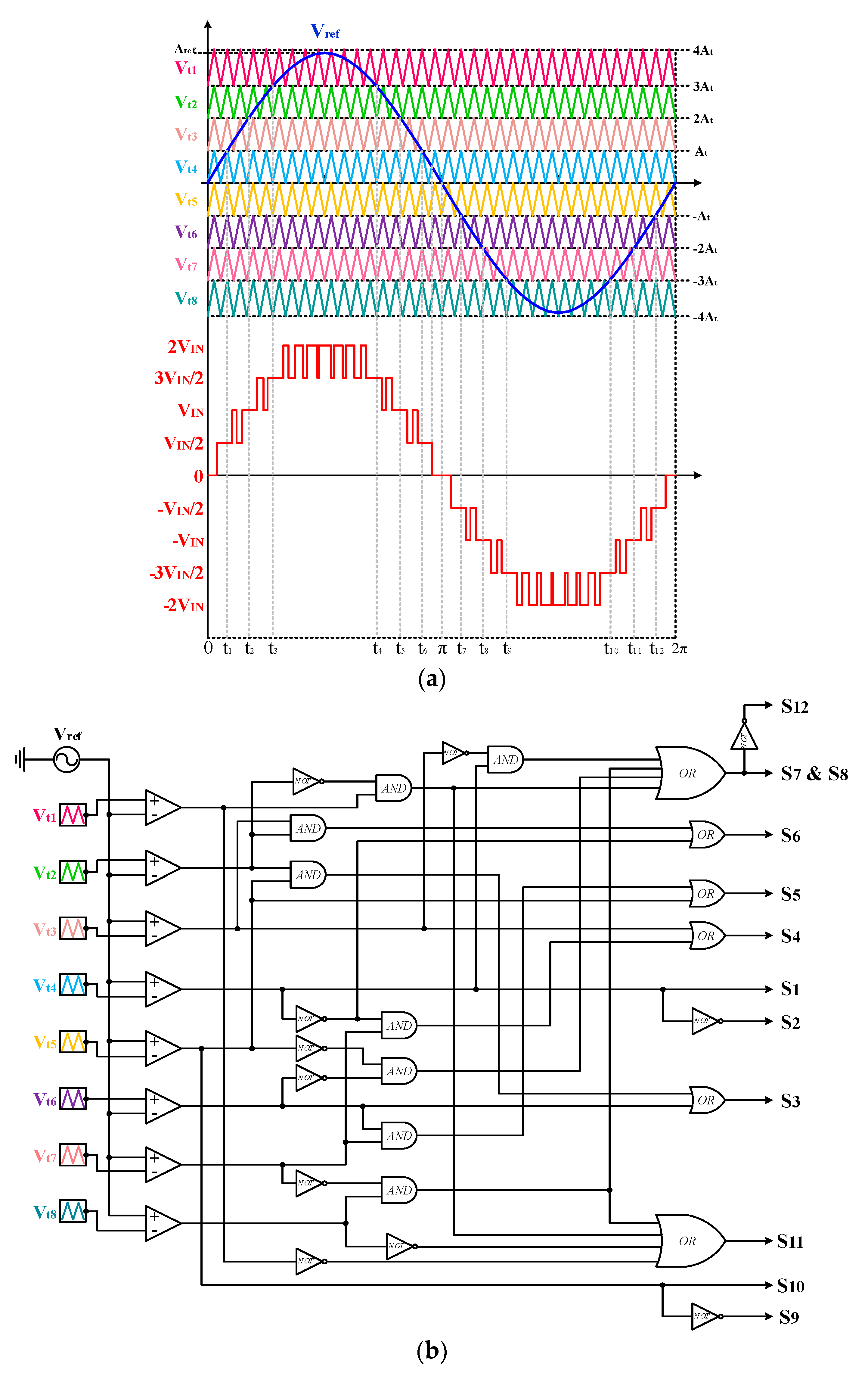
Therein, phase disposition PWM technique is applied to control each IGBT of the proposed topology. To do this, eight triangular carriers (Vt1 to Vt8) arranged with shifts in amplitudes are required (see Figure 3a). It should be noted that they are the same in amplitude (At), frequency (ft) and phase [16,17]. The carriers are compared to a reference waveform (Vref) which results in generating appropriate fire pulses for all switches. For instance, S11 is turned on when Vref > Vt1 or Vt2 < Vref < Vt1 or Vt8 < Vref < Vt7 or Vref <Vt8. In other words, S11 must be turned on when S1: ON, S4: ON, S3: OFF (or S2: ON, S3: ON, S4: OFF), which can be observed in Figure 2. Similarly, S12 is turned on when Vref > Vt1 or Vt3 < Vref < Vt2 or Vt5 < Vref < Vt4 or Vt7 < Vref < Vt6 or Vref < Vt8. In other words, S12 must be turned on when S7 and S8 are OFF (see Figure 2). Further clarification concerning switching strategy is brought up in Figure 3b and Table 3.

4. Loss Distribution and Thermal Modeling

4.1. Power Loss Analysis

The power loss for a multilevel inverter is composed of three parts including PC, PS and PR which are elaborated as follows:

4.1.1. Conduction Loss (PC)

PC is caused by parasitic resistance (i.e., ON-state resistance of the switch (RS) and its parallel diode (RD), capacitor internal resistance (RC)) involved in the current paths [18]. Table 4 shows the equivalent value of the parasitic resistance (Req) existing in each voltage level. It should be noted that in the present work RS, RD, and RC are considered equal to 0.27 Ω, 0.05 Ω, and 0.03 Ω, respectively.
If |Vref| < At, the output voltage switches between 0 and +VIN/2 (see Figure 3a). Consequently, the output current passes through two switches and two diodes (three switches, two diodes, and one capacitor) during 0 (+VIN/2) level, as depicted in Table 4. In this case, the energy dissipated within 0 < t < t1 (t6 < t < t7 or t12 < t < 2π) is attained by Equation (1) in which At, Aref, and fref are considered equal to 0.25, 0.9, and 50 Hz, respectively [18]. Moreover, t1 is calculated as follows:
E 0 & V I N / 2 = 0 t 1 [ I L o a d s i n ( 2 π f r e f t ) ] 2 × [ ( 3 R S + 2 R D + R C ) A r e f s i n ( 2 π f r e f t ) A t + ( 2 R S + 2 R D ) ( 1 A r e f s i n ( 2 π f r e f t ) A t ) ] d t = 2.04 × 10 5 × ( P o u t V I N ) 2
t 1 = s i n 1 ( A t A r e f ) 2 π f r e f = s i n 1 ( 0.25 0.9 ) 100 π = 9 × 10 4 s e c .
Similarly, the energy losses that occurred in other time intervals are calculated by Equations (3)–(8).
E V I N / 2 & V I N = t 1 t 2 [ I L o a d s i n ( 2 π f r e f t ) ] 2 × [ ( 3 R S + R D ) A r e f s i n ( 2 π f r e f t ) A t A t + ( 3 R S + 2 R D + R C ) ( 1 A r e f s i n ( 2 π f r e f t ) A t A t ) ] d t = 2.03 × 10 4 × ( P o u t V I N ) 2
t 2 = s i n 1 ( 2 A t A r e f ) 2 π f r e f = s i n 1 ( 0.5 0.9 ) 100 π = 1.87 × 10 3 s e c .
E V I N & 3 V I N / 2 = t 2 t 3 [ I L o a d s i n ( 2 π f r e f t ) ] 2 × [ ( 5 R S + R D + R C ) A r e f s i n ( 2 π f r e f t ) 2 A t A t + ( 3 R S + R D ) ( 1 A r e f s i n ( 2 π f r e f t ) 2 A t A t ) ] d t = 7.2 × 10 4 × ( P o u t V I N ) 2
t 3 = s i n 1 ( 3 A t A r e f ) 2 π f r e f = s i n 1 ( 0.75 0.9 ) 100 π = 3.1 × 10 3 s e c .
E 3 V I N / 2 & 2 V I N = t 3 t 4 [ I L o a d s i n ( 2 π f r e f t ) ] 2 × [ ( 6 R S + 2 R C ) A r e f s i n ( 2 π f r e f t ) 3 A t A t + ( 5 R S + R D + R C ) ( 1 A r e f s i n ( 2 π f r e f t ) 3 A t A t ) ] d t = 0.0051 × ( P o u t V I N ) 2
t 4 = π s i n 1 ( 3 A t A r e f ) 2 π f r e f = π s i n 1 ( 0.75 0.9 ) 100 π = 6.86 × 10 3 s e c .
Due to quarter-wave symmetry of the output voltage, the total conduction loss for the proposed 9 L topology is:
P C = ( 4 E 0 & V I N / 2 + 4 E V I N / 2 & V I N + 4 E V I N & 3 V I N / 2 + 2 E 3 V I N / 2 & 2 V I N ) × f r e f = 0.69 × ( P o u t V I N ) 2

4.1.2. Switching Loss (PS)

The overlap of switch voltage and current during rise and fall times (i.e., ton and toff) leads to PS, which is highly proportional to the fS. The turn-on and turn-off power loss of the switch S are attained by [19]:
P S , o n = f S 0 t o n v S ( t ) i S ( s ) d t = f S 0 t o n ( V S t o n t ) ( I S o n t o n ( t t o n ) ) d t = 1 6 f S V S I S o n t o n
P S , o f f = f S 0 t o f f v S ( t ) i S ( t ) d t = f S 0 t o f f ( V S t o f f t ) ( I S o f f t o f f ( t t o f f ) ) d t = 1 6 f S V S I S o f f t o f f
In which ISon (ISoff) is the switch current after (before) turning on (off). Considering ton = toff = 58 ns and ft = 4 kHz, PS for all the switches is obtained as follows:
P S j , o n = P S j , o f f = 1 6 × 1 2 × 4 × 10 3 × V I N × I L o a d π × 58 × 10 9 = 6.15 × 10 6 × P o u t , j = 1 , 2 , 9 , 10 , 11
P S j , o n = P S j , o f f = 1 6 × 4 × 10 3 × V I N × I L o a d π × 58 × 10 9 = 12.3 × 10 6 × P o u t , j = 3 , 4 , 5 , 6
P S j , o n = P S j , o f f = 1 6 × 1 2 × 4 × 10 3 × V I N 2 × I L o a d π × 58 × 10 9 = 3.07 × 10 6 × P o u t , j = 7 , 8
P S 12 , o n = P S 12 , o f f = 1 6 × 1 2 × 4 × 10 3 × V I N 2 × I L o a d π × 58 × 10 9 = 3.07 × 10 6 × P o u t
Consequently, the total switching loss for the presented 9 L inverter is calculated by:
P S = j = 1 N s w i t c h ( P S j , O N + P S j , O F F ) = 178 × 10 6 × P o u t

4.1.3. Power Loss Generated by Capacitor Voltage Ripple (PR)

PPR is due to the voltage difference between the capacitor and input DC source during the charging periods. Generally, the maximum discharging value of each capacitor in a switched-capacitor circuit is attained by [13,18]:
Δ Q C = t c t d I L o a d S i n ( 2 π f r e f t ) d t
where [tc, td] is the discharging interval of each capacitor. According to Figure 2a and Figure 3a, the maximum discharging period of C1 (or C2) is equal to [t3, t4]. Thus, considering maximum acceptable voltage drop across C1 (or C2) equal to ΔVripple, the capacitance of each capacitor is calculated by [13,18]:
C Δ Q C Δ V r i p p l e × 0.5 V I N
For example, considering Pout = 1.4 kW (ILoad = 7 A, VIN=200 V) and ΔVripple = 10%, the capacitances for the proposed inverter are obtained as follows:
C 1 = C 2 = 0.0031 0.00686 7 × S i n ( 100 π t ) d t 0.1 × 100 = 0.024 10 = 2400 μ F
It also should be noted that nominal voltage of the capacitors is equal to VIN/2 (see Figure 2). Consequently, PR for the proposed topology is attained as follows:
P R = f r e f 2 ( i = 1 2 C i ( Δ V r i p p l e × 0.5 V I N ) 2 ) = 50 × ( 0.0031 0.00686 I L o a d s i n ( 100 π t ) d t × Δ V r i p p l e × 0.5 V I N ) = 0.088 × Δ V r i p p l e × P o u t
Therefore, considering Equations (9), (16), and (20), the efficiency is calculated by Equation (21).
η = P o u t P i n = P o u t P o u t + P C + P S + P R
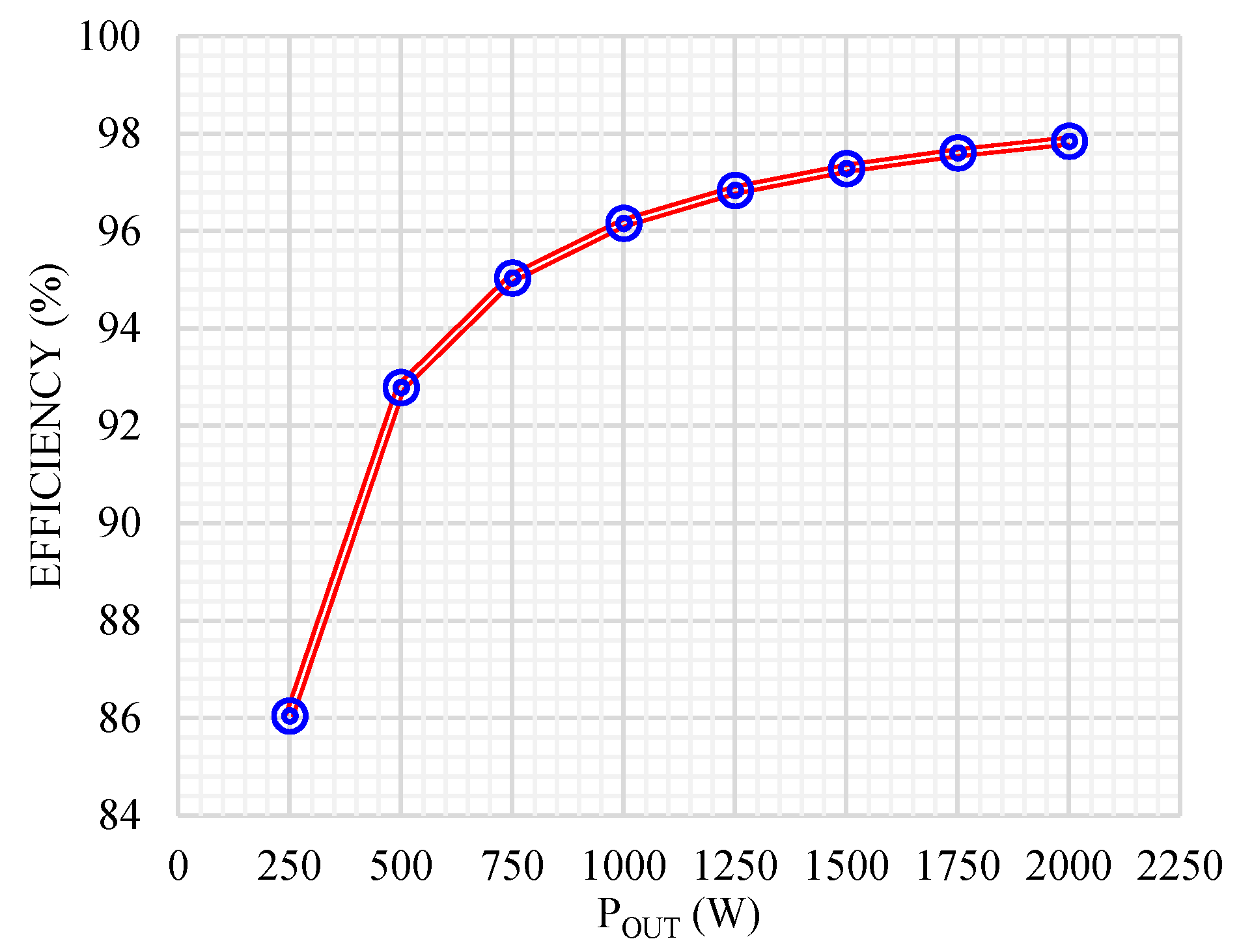
Theoretical efficiency of the proposed inverter has been calculated at different output power and presented in Figure 4. It is observed that there is a marked rise in the efficiency by increasing the output power.

4.2. Thermal Model

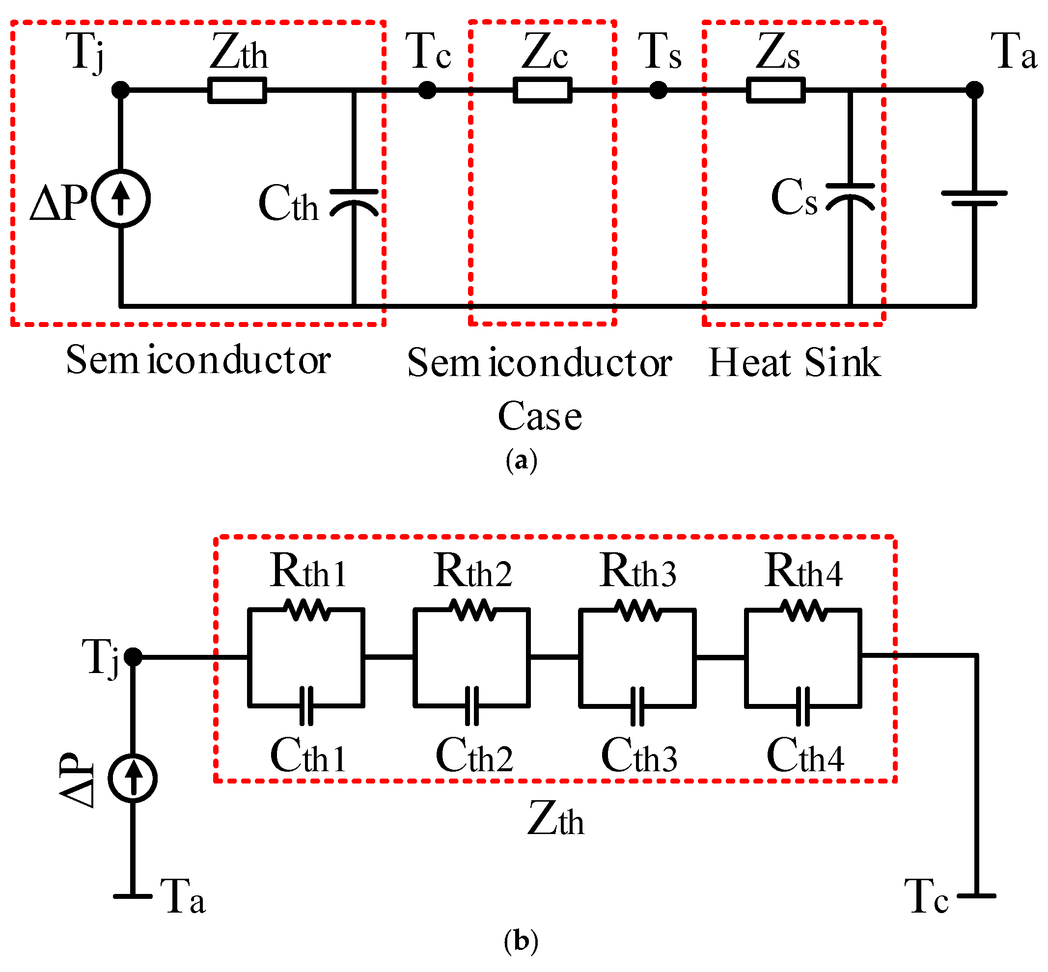
Heat distribution through semiconductor components is caused by power loss, which leads to an increasing of Tj [20]. This temperature, for safety reasons, should be monitored and kept within a specified range during the inverter operation. Figure 5a illustrates the thermal model implemented for a single semiconductor, in which the thermal impedance between junction and case (Zth) is considered a four-layer foster network (see Figure 5b) [21,22]. It should be noted that Zc and Zs are the thermal impedances from the case to the heat sink and from the heat sink to the ambient, respectively. These are found on the manufacturer datasheet.
Modelling loss dissipation of the proposed 9 L inverter in MATLAB/Simulink yields the junction temperature of the power electronic devices [23,24,25]. Herein, Ta is considered equal to 40 °C and the PM75CLA060 switch produced by Mitsubishi Electric is chosen in the thermal estimation.
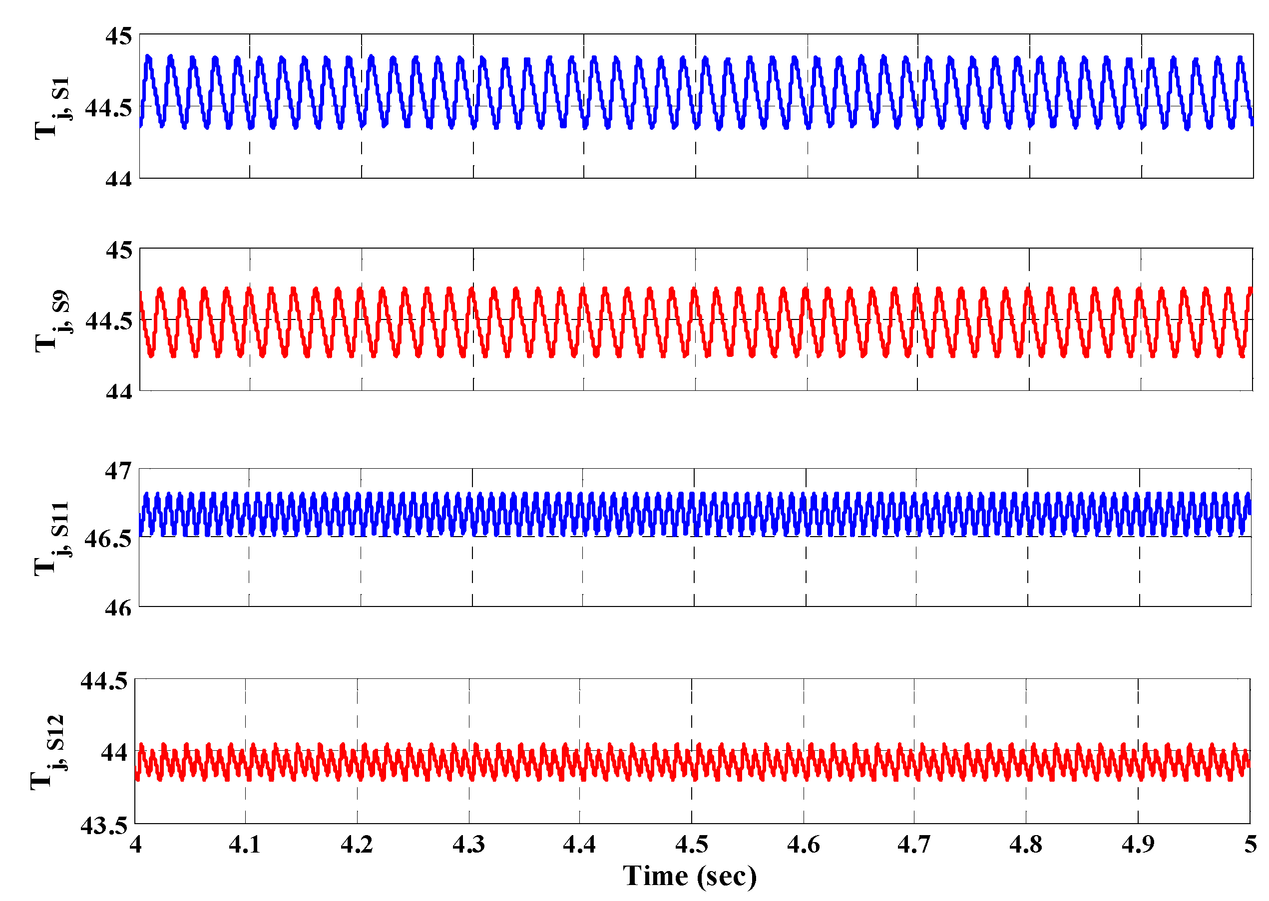
The estimated Tj of some power switches employed in the proposed inverter at 20 kW output power is illustrated in Figure 6. It can be observed that S12 has the lowest Tj (approximately 43.9 °C), while this temperature approaches 46.7 °C for S11.

5. Simulation and Experimental Results

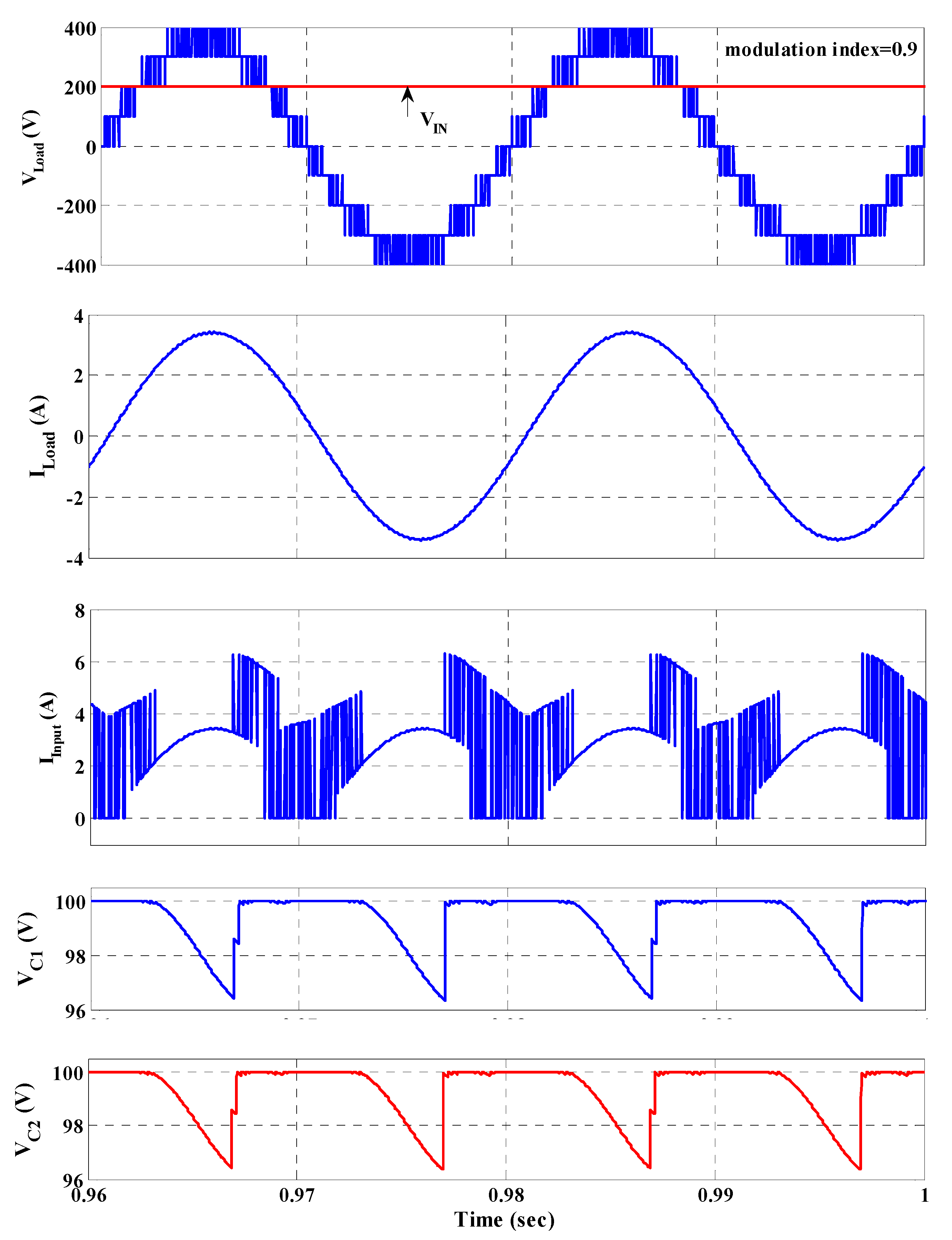
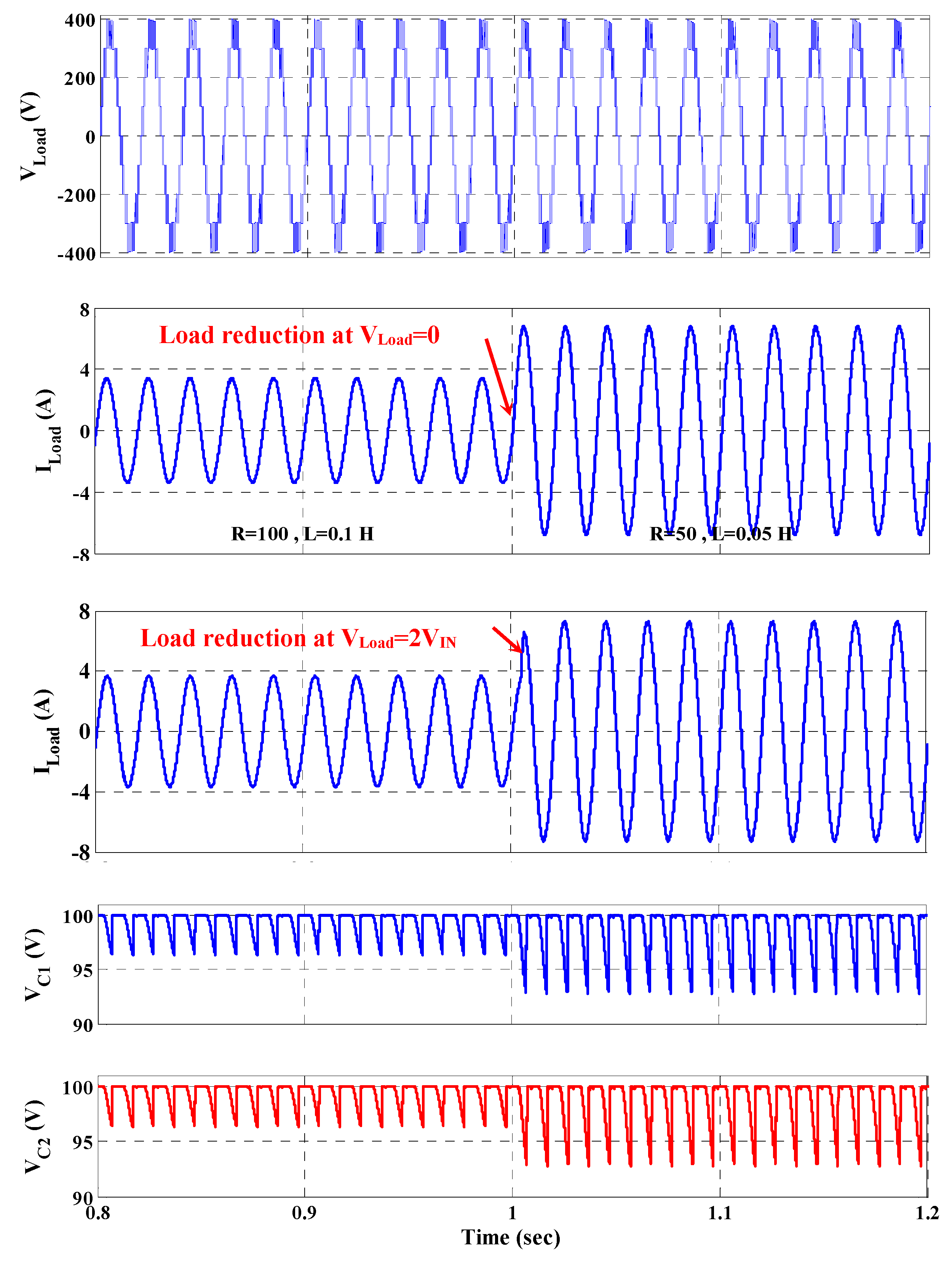
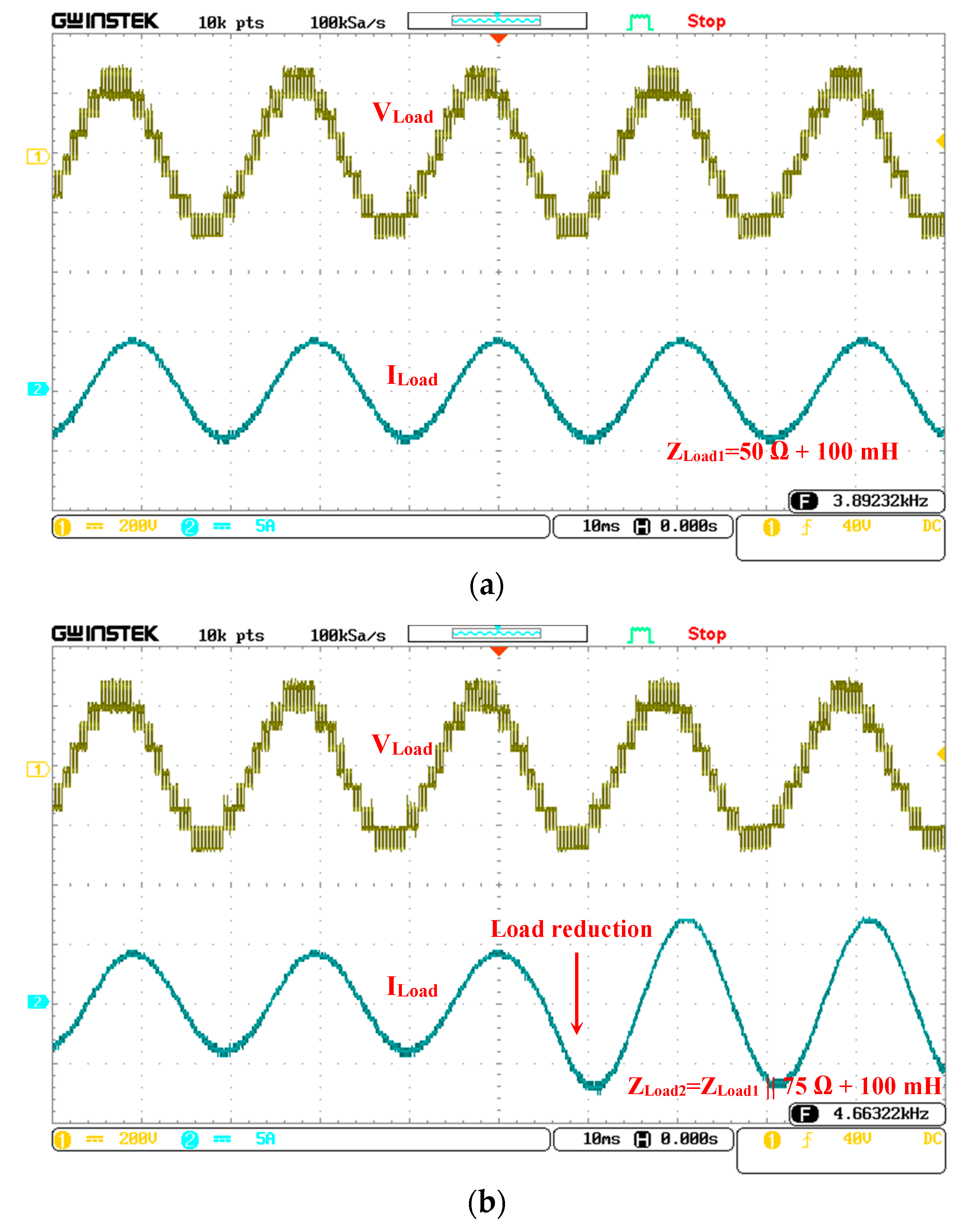
Simulations have been conducted in MATLAB for steady-state and transient modes, as presented below. Figure 7 shows the inverter output voltage/current and capacitors voltage at resistive-inductive load (ft = 4 kHz, C1 = C2 = 2300 µF, R = 100 Ω, L = 100 mH). These results confirm the flawless performance and self-balanced ability of the presented 9 L inverter. Moreover, the value of the input DC source is selected at 200 V. Thus, the capacitors and output voltages reach 100 V and 400 V, respectively. The proposed topology has also been simulated under step change in the load, and the results are presented in Figure 8. As can be observed, the voltage ripple across the capacitors rises promptly from 3.5% to 7.2% by decreasing the load impedance. Once again, these figures verify the inherent capacitor voltage balancing ability during inverter operation.
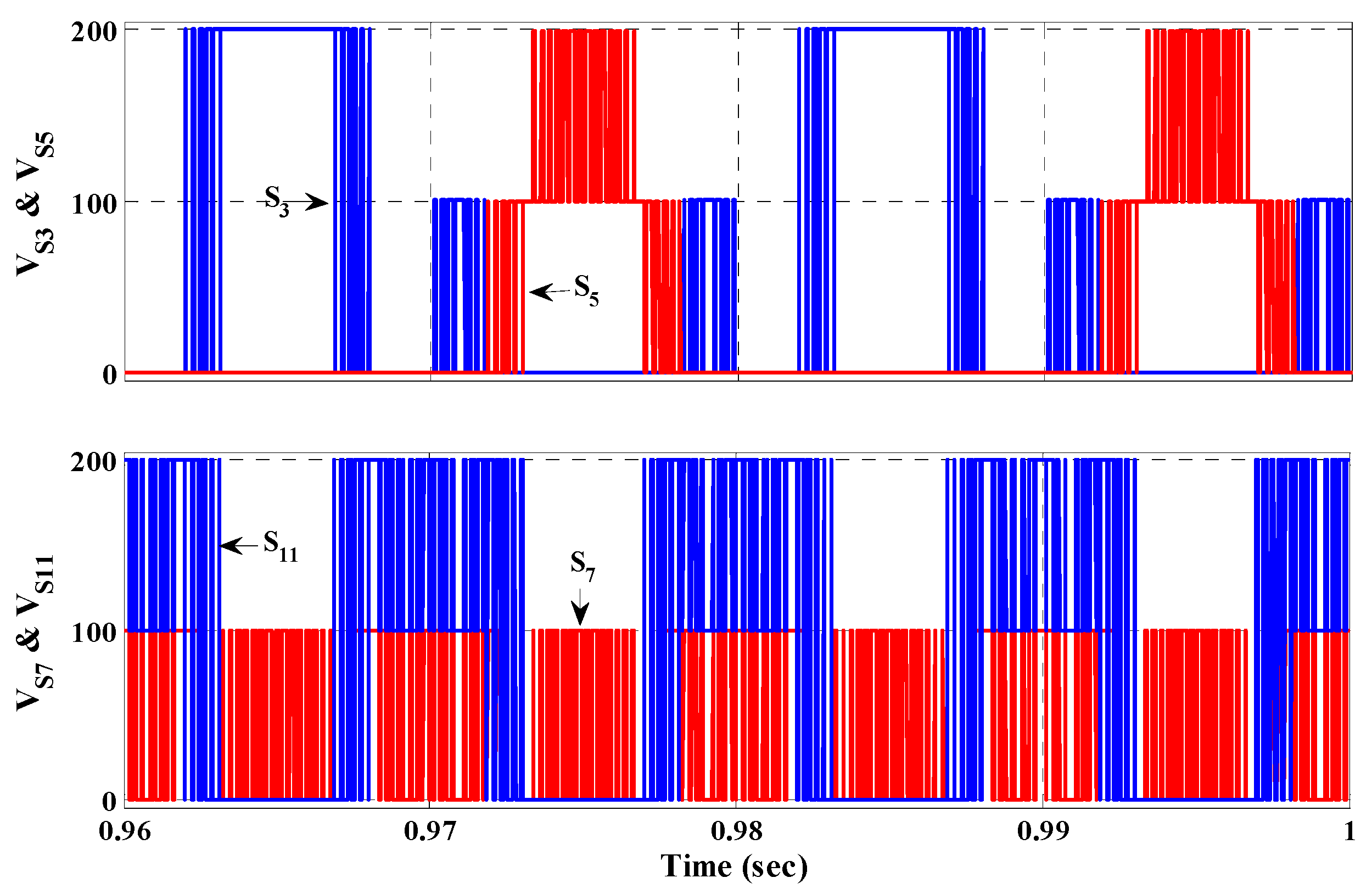
Figure 9 shows the voltage waveforms across some power switches employed in the proposed topology. It is clear that S3, S5, and S11 (also S1, S2, S4, S6, S9 and S10) must withstand voltages equal to the input DC source (i.e., 200 V). Other switches (S7, S8 and S12), however, block voltages equal to half the input DC source (i.e., 100 V). To sum up, unlike topologies with end side H-bridge, none of the switches required for the proposed inverter tolerate maximum output voltage (i.e., 400 V).
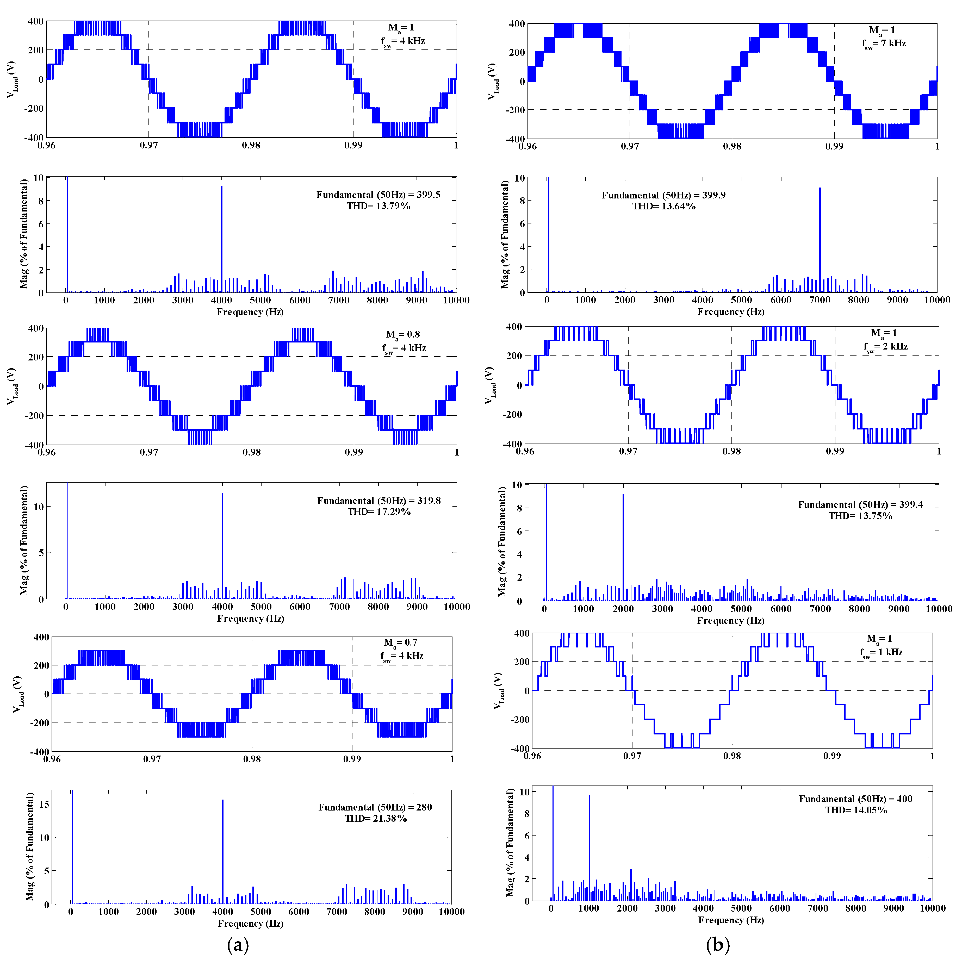
Furthermore, the effect of different modulation indexes and switching frequencies on the operation of the proposed inverter is shown in Figure 10. It is observed that the inverter output voltage has lower THD at higher modulation index (and higher switching frequency). Moreover, the fundamental component of output voltage is decreased at lower modulation index.
To validate the high performance of the proposed model, a low-power prototype of the proposed inverter has been implemented and tested. Accordingly, a Texas Instruments (TMS320F28335) fixed-point DSP control board generated gate pulses for employed switches (IRFP460 500 V/20 A). Moreover, the value of capacitances and input DC source are selected at 2300 µF and 140 V, respectively. Figure 11 illustrates the results obtained from the hardware implementation of the proposed inverter model under steady-state and transient operating conditions. These figures fully confirm the flawless performance of the proposed inverter.

6. Conclusions

Herein, the operating principle of a new 9 L inverter has been discussed and confirmed experimentally. The comparative analysis depicted that the presented topology not only reduces the number of semiconductors/DC links required for generating a 9 L voltage waveform, but also employs IGBTs with lower PIV. These merits lead to a high compactness and cost reduction of the conversion system. Due to the intrinsic self-voltage balancing ability, there is no need for complex modulation methods. Thereupon, it enjoys simple control and implementation. Furthermore, the theoretical efficiency demonstrated that the presented configuration has higher efficiency by increasing output power (up to 2000 W). Eventually, the feasibility and effectiveness of the proposed model was verified by the simulation and experimental results.

Author Contributions

All authors contributed equally to this work and all authors have read and approved the final manuscript.

Funding

This research received no external funding.

Conflicts of Interest

The authors declare no conflicts of interest.

Nomenclature

MLIsMultilevel inverters
CHBCascaded H-bridge
NPCNeutral point clamped
FCFlying capacitor
TSVTotal standing voltage (V)
PIVPeak inverse voltage (V)
PWMPulse width modulation
DSPDigital signal processor
VIN and IINInput voltage (V) and current (A) of the inverter
VLoad and ILoadMaximum load voltage (V) and current (A)
VtTriangular carrier of the PWM modulation
VrefReference waveform of the PWM modulation
VS and ISVoltage (V) and current (A) of the switch S
ΔVrippleVoltage ripple across each capacitor (V)
ΔQCMaximum discharging value of the capacitor C
NNumber of power switches with the same PIV
MNumber of cascaded modules
At and ftAmplitude and frequency of the triangular carriers (Vt)
Aref and frefAmplitude and frequency of the reference waveform (Vref)
PCConduction loss (W)
PSSwitching loss (W)
PRPower loss caused by capacitor voltage ripple (W)
PS, on and PS, offTurn-on and turn-off power loss of the switch S (W)
PoutInverter output power (W)
RS and RDON-state resistance of the switch S and its parallel diode (Ω)
RCCapacitor internal resistance (Ω)
ReqEquivalent value of the parasitic resistance in each voltage level (Ω)
R and LResistance (Ω) and inductance (H) of the load
ton and toffRise and fall times of the switch S (s)
fSSwitching frequency (Hz)
TjSemiconductor junction temperature (°C)
TcSemiconductor case temperature (°C)
TsHeat sink temperature (°C)
TaAmbient temperature (°C)
ZthThermal impedance between junction and case of the semiconductor
ZcThermal impedance between semiconductor case and its heat sink
ZsThermal impedance between heat sink and ambient

References

  1. Kouro, S.; Malinowski, M.; Gopakumar, K.; Pou, J.; Franquelo, L.G.; Wu, B.; Rodriguez, J.; Perez, M.A.; Leon, J.I. Recent Advances and Industrial Applications of Multilevel Converters. IEEE Trans. Ind. Electron. 2010, 57, 2553–2580. [Google Scholar] [CrossRef]
  2. Yuan, X. Derivation of Voltage Source Multilevel Converter Topologies. IEEE Trans. Ind. Electron. 2017, 64, 966–976. [Google Scholar] [CrossRef] [Green Version]
  3. Rodriguez, J.; Franquelo, L.G.; Kouro, S.; Leon, J.I.; Portillo, R.C.; Prats, M.A.M.; Perez, M.A. Multilevel Converters: An Enabling Technology for High-Power Applications. Proc. IEEE 2009, 97, 1786–1817. [Google Scholar] [CrossRef]
  4. Gupta, K.K.; Ranjan, A.; Bhatnagar, P.; Kumar Sahu, L.; Jain, S. Multilevel Inverter Topologies with Reduced Device Count: A Review. IEEE Trans. Power Electron. 2016, 31, 135–151. [Google Scholar] [CrossRef]
  5. Leon, J.I.; Vazquez, S.; Franquelo, L.G. Multilevel Converters: Control and Modulation Techniques for Their Operation and Industrial Applications. Proc. IEEE 2017, 105, 2066–2081. [Google Scholar] [CrossRef]
  6. Akagi, H. Multilevel Converters: Fundamental Circuits and Systems. Proc. IEEE 2017, 105, 2048–2065. [Google Scholar] [CrossRef]
  7. Wu, B.; Narimani, M. Diode-Clamped Multilevel Inverters. In High-Power Converters and AC Drives; Wiley-IEEE Press: New York, NY, USA, 2017. [Google Scholar]
  8. Khounjahan, H.; Abapour, M.; Zare, K. Switched-Capacitor Based Single Source Cascaded H-bridge Multilevel Inverter Featuring Boosting Ability. IEEE Trans. Power Electron. 2018, 34, 1113–1124. [Google Scholar] [CrossRef]
  9. Lee, S. Single-Stage Switched-Capacitor Module (S3CM) Topology for Cascaded Multilevel Inverter. IEEE Trans. Power Electron. 2018, 33, 8204–8207. [Google Scholar] [CrossRef]
  10. Choi, J.S.; Kang, F.S. Seven-Level PWM Inverter Employing Series-Connected Capacitors Paralleled to a Single DC Voltage Source. IEEE Trans. Ind. Electron. 2015, 62, 3448–3459. [Google Scholar]
  11. Hinago, Y.; Koizumi, H. A Switched-Capacitor Inverter Using Series/Parallel Conversion. IEEE Int. Symp. Circuits Syst. 2010, 62, 3188–3191. [Google Scholar]
  12. Wang, K.; Zheng, Z.; Wei, D.; Fan, B.; Li, Y. Topology and Capacitor Voltage Balancing Control of a Symmetrical Hybrid Nine-Level Inverter for High-Speed Motor Drives. IEEE Trans. Ind. Appl. 2017, 53, 5563–5572. [Google Scholar] [CrossRef]
  13. Taghvaie, A.; Adabi, J.; Rezanejad, M. A Self-Balanced Step-Up Multilevel Inverter Based on Switched-Capacitor Structure. IEEE Trans. Power Electron. 2018, 33, 199–209. [Google Scholar] [CrossRef]
  14. Lee, S.S.; Sidorov, M.; Lim, C.S.; Idris, N.R.N.; Heng, Y.E. Hybrid Cascaded Multilevel Inverter (HCMLI) With Improved Symmetrical 4-level Submodule. IEEE Trans. Power Electron. 2018, 33, 932–935. [Google Scholar] [CrossRef]
  15. Lee, S.S. A Single-Phase Single-Source 7-Level Inverter with Triple Voltage Boosting Gain. IEEE Access 2018, 6, 30005–30011. [Google Scholar] [CrossRef]
  16. McGrath, B.P.; Holmes, D.G. Multicarrier PWM Strategies for Multilevel Inverters. IEEE Trans. Ind. Electron. 2002, 49, 858–867. [Google Scholar] [CrossRef]
  17. Mei, J.; Xiao, B.; Shen, K.; Tolbert, L.M.; Zheng, J.Y. Modular Multilevel Inverter with new Modulation Method and its Application to Photovoltaic Grid-Connected Generator. IEEE Trans. Power Electron. 2013, 28, 5063–5073. [Google Scholar] [CrossRef]
  18. Tsunoda, A.; Hinago, Y.; Koizumi, H. Level-and Phase-Shifted PWM for Seven-Level Switched-Capacitor Inverter Using Series/Parallel Conversion. IEEE Trans. Ind. Electron. 2014, 61, 4011–4021. [Google Scholar] [CrossRef]
  19. Barzegarkhoo, R.; Moradzadeh, M.; Zamiri, E.; Kojabadi, H.M.; Blaabjerg, F. A new Boost Switched-Capacitor Multilevel Converter with Reduced Circuit Devices. IEEE Trans. Power Electron. 2018, 33, 6738–6754. [Google Scholar] [CrossRef]
  20. Albarbar, A.; Batunlu, C. Thermal Analysis of Power Electronic Devices Used in Renewable Energy Systems; Springer-Cham: Cham, Switzerland, 2018. [Google Scholar]
  21. Ma, K.; Muñoz-Aguilar, R.S.; Rodriguez, P.; Blaabjerg, F. Thermal and Efficiency Analysis of Five-Level Multilevel-Clamped Multilevel Converter Considering Grid Codes. IEEE Trans. Ind. Appl. 2014, 50, 415–423. [Google Scholar] [Green Version]
  22. Lixiang, W.; McGuire, J.; Lukaszewski, R.A. Analysis of PWM Frequency Control to Improve the Lifetime of PWM Inverter. IEEE Trans. Ind. Electron. 2011, 47, 922–929. [Google Scholar] [CrossRef]
  23. Ma, K.; Bahman, A.S.; Beczkowski, S.; Blaabjerg, F. Complete Loss and Thermal Model of Power Semiconductors Including Device Rating Information. IEEE Trans. Power Electron. 2015, 30, 2556–2569. [Google Scholar] [CrossRef]
  24. Rajapakse, A.; Gole, A.; Jayasinghe, R. An Improved Representation of FACTS Controller Semiconductor Losses in EMTP-Type Programs Using Accurate Loss-Power Injection Into Network Solution. IEEE Trans. Power Del. 2009, 24, 381–389. [Google Scholar] [CrossRef]
  25. Tu, Q.; Xu, Z. Power Losses Evaluation for Modular Multilevel Converter with Junction Temperature Feedback. In Proceedings of the IEEE Power and Energy Society General Meeting, Detroit, MI, USA, 24–29 July 2011; pp. 1–7. [Google Scholar]
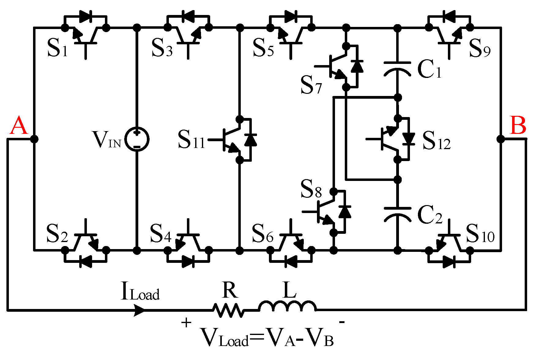
Figure 1. The proposed 9 L topology.
Energies 12 00207 g001
Figure 2. Switching states of the proposed inverter, (a) +2VIN, (b) +3VIN/2, (c) +VIN, (d) +VIN/2, (e) 0; (f) −VIN/2, (g) −VIN, (h) −3VIN/2, (i) −2VIN.
Energies 12 00207 g002
Figure 3. (a) PWM technique, (b) Logic schematic.
Energies 12 00207 g003
Figure 4. Inverter efficiency at different power output.
Energies 12 00207 g004
Figure 5. (a) Semiconductor thermal model; (b) foster network of Zth.
Energies 12 00207 g005
Figure 6. The estimated Tj at 20 kW output power.
Energies 12 00207 g006
Figure 7. Operation of the presented model under constant load.
Energies 12 00207 g007
Figure 8. Operation of the presented model under sudden load reduction.
Energies 12 00207 g008
Figure 9. Voltages across the switches.
Energies 12 00207 g009
Figure 10. The effect of (a) modulation index on the VLoad, (b) switching frequency on the VLoad.
Energies 12 00207 g010
Figure 11. Output voltage/current under, (a) constant load; (b) step change in the load.
Energies 12 00207 g011
Table 1. Comparison of the proposed topology with other recently presented inverters.
Comparison ItemCHB (Con.)[11] (2010)[12] (2017)[13] (2018)[14] (2018)[15] (2018)Proposed
Level99999798M * + 1
Switch1613121910161212M
Capacitor-343-222M
DC source4111411M
N * × PIV16 × 1VIN4 × 4VIN
9 × 1VIN
4 × 4VIN
8 × 1VIN
19 × 1VIN4 × 4VIN
2 × 3VIN
4 × 1VIN
16 × 1VIN9 × VIN
3 × VIN/2
9M × VIN
3M × VIN/2
TSV16VIN25VIN24VIN19VIN26VIN16VIN21VIN/2M × (21VIN/2)
M *: Number of cascaded modules.
Table 2. Price Comparison of the Single-Source MLIs.
PartPart NumberVoltage Rating (V)Unit Price * (€)[11][12][13][15]Proposed
MOSFETsSTW40NF202003.539819-3
SUP40N25-60-E32504.43---169
FQL40N504507.73-----
SIHG47N60AEFGE36007.8244---
CapacitorsE32D151HPN472TEE3M15023.00324-2
B43713F2478M00025039.39---2-
ALS31A472NF35035048.83-2---
Gate driverIRS21271SPBF-1.341312191412
Total cost (€) 149.47219.26184.53168.42112.54
* Source: www.mouser.com.
Table 3. On-State IGBTs for Each Level.
Relationship between the Carriers and VrefON-State IGBTsLevels
Vref > Vt1S1-S4-S5-S10-S11-S12+4VIN
Vt2 < Vref < Vt1S1-S4-S5-S7-S8-S10-S11+3VIN
Vt3 < Vref < Vt2S1-S3-S4-S5-S6-S10-S12+2VIN
Vt4 < Vref < Vt3S1-S3-S5-S7-S8-S10+1VIN
Vt5 < Vref < Vt4S2-S3-S4-S5-S6-S10-S120
Vt6 < Vref < Vt5S2-S4-S6-S7-S8-S9−1VIN
Vt7 < Vref < Vt6S2-S3-S4-S5-S6-S9-S12−2VIN
Vt8 < Vref < Vt7S2-S3-S6-S7-S8-S9-S11−3VIN
Vref < Vt8S2-S3-S6-S9-S11-S12−4VIN
Table 4. Req in Each Step.
Output LevelReq (Ω)
02RS + 2RD = 0.64
±VIN/23RS + 2RD + RC = 0.94
±VIN3RS + RD = 0.86
±3VIN/25RS + RD + RC = 1.43
±2VIN6RS + 2RC = 1.68