Article

Double Stage Double Output DC–DC Converters for High Voltage Loads in Fuel Cell Vehicles

Center for Bioenergy and Green Engineering, Department of Energy Technology, Aalborg University, 6700 Esbjerg, Denmark
*
Author to whom correspondence should be addressed.
Energies 2019, 12(19), 3681; https://doi.org/10.3390/en12193681
Submission received: 1 July 2019 / Revised: 14 September 2019 / Accepted: 19 September 2019 / Published: 26 September 2019

Abstract

:
This article aims to enhance the output voltage magnitude of fuel cells (FCs), since the actual generation is low. The traditional technique is too complicated and has a cascaded or parallel connection solution to achieve high voltage for multiple loads in vehicles. In this case, electronic power converters are a viable solution with compact size and cost. Hence, double or multiple output DC–DC converters with high voltage step up are required to feed multiple high voltage loads at the same time. In this article, novel double stage double output (DSDO) DC–DC converters are formulated to feed multiple high voltage loads of FC vehicular system. Four DSDO DC–DC converters called DSDO L–L, DSDO L-2L, DSDO L-2LC, and DSDO L-2LC are developed in this research work and all the converters are derived based on the arrangement of different reactive networks. The primary power circuitry, conceptual operation, and output voltage gain derivation are given in detail with valid proof. The proposed converters are compared with possible parallel combinations of conventional converters and recently available configuration. Comprehensive numerical simulation and experimental prototype results show that our theoretical predictions are valid and that the configuration is applicable for real time application in FC technologies for ‘more-electric vehicles’.

1. Introduction

In electric grid, hybrid ‘more-electric vehicles’, automobile high-intensity discharge headlamps, uninterruptible power supply, and luxury loads application multiport and multilevel power converters popular solutions [1,2,3,4]. Some advanced predictive control based on the multilevel converter is also proposed for energy storage [5,6]. Fuel cells have many features, including compatibility, size, and modularity [7,8]. However, the amalgamation of series and parallel FCs is not a suitable solution for generating high DC voltage/current. Trade-off loss increases the cost of the system and requires a large space. Furthermore, the major obstacles facing FC technology are durability, low generated voltage, and to fulfill the voltage demand of high voltage loads in FC vehicles. In such cases, power electronic DC–DC converters with high voltage conversion ratios and high efficiency play a pivotal control role [9,10,11,12]. Theoretically, a moderate or high output voltage is obtained from a traditional boost converter by operating in an extreme duty cycle. Adverse effects at extreme duty ratio lead to reduced controllability, increased switching losses, high conduction losses, large current ripple, high current and voltage ratings, and reverse diode recovery problems [13,14,15,16]. Consequently, traditional DC–DC converters are not suitable candidates for FC electric vehicle applications.
Previous research has achieved high voltage conversion ratio by using a cascaded traditional boost converter configuration. However, cascaded converter configurations have low efficiency and high cost due to the increased number of high voltage/current rating semiconductor devices and reactive elements [17,18]. Further, for implementation, they need complex control logic and increased driver modules to protect and control the semiconductor devices. Quadratic boost converters achieve a high voltage conversion ratio, but high current/voltage rating components/devices and the internal resistance of the inductors limits the output voltage [19]. Multistage diode/capacitor-based DC–DC converters have been proposed to achieve high voltage gain [20,21,22,23,24]. However, multiple discharging/charging loops of the capacitors lead to increased conduction loss, cost, and size, and reduced efficiency due to their parasitic nature. Converters have been proposed to get multiple outputs from a single input source by using push-pull, half-bridge, full-bridge, and fly-back converter topologies [25,26,27]. In all cases, high voltage is obtained with a high transformer rating on the primary side. Therefore, these converters cannot provide a proper solution for low weight/cost applications.
The parallel configurations of traditional converters such as boost, buck-boost, Cuk, single ended primary inductance converter (SEPIC), and ZETA can be possible solutions to achieve multiple outputs. The power circuitry of possible configurations without common front-end structure are shown in Figure 1a–e. These configurations provide two outputs using two different control switches. However, the voltage gain is not significantly improved, even when using a large number of components and devices. Furthermore, in order to reduce the component or device counts, common front-end structure can be a solution, as shown in Figure 1f–j. These configurations provide dual output using common front-end structures. However, only a few input side components are used, the device count is reduced, and the voltage gain is limited. Moreover, the current rating of the components is increased due to the common structure. In order to reduce the component count, hybrid converters are another possible solution. Moreover, hybrid Cuk, SEPIC, and ZETA converter configurations can achieve multiple outputs. A combination of Cuk and SEPIC converter structure was employed in [28]. Figure 2a shows the SEPIC-Cuk converter circuitry with common front-end design and dual output. A combination of ZETA and buck-boost converter structure was employed in [29].
Figure 2b shows the circuitry of a ZETA–Buck-boost converter with common front-end structure and two outputs. The combination of Cuk and boost converters is employed in [30]. The circuitry of a boost-Cuk converter with common front-end and two outputs is shown in Figure 2c. The voltage conversion ratio of these topologies is limited. Furthermore, efforts have been made to reduce the switching and to obtain multiple outputs [31,32,33]. However, these converters have low voltage conversion ratio and are more suitable for low-power applications. The “X–Y converter family” has been proposed for high voltage output and has single switching and a capacitor stack at the output side [34,35,36,37,38]. The block diagram of the X–Y converter family is depicted in Figure 2d. Notable, in XY converters, the X converter is directly connected to the input supply, and the Y converter is fed from the output voltage of the X converter. The output voltage of an X–Y converter is the sum of the output voltages of the X and Y converters. In order to achieve multiple outputs and high voltage conversion ratio, this article contributes the following:
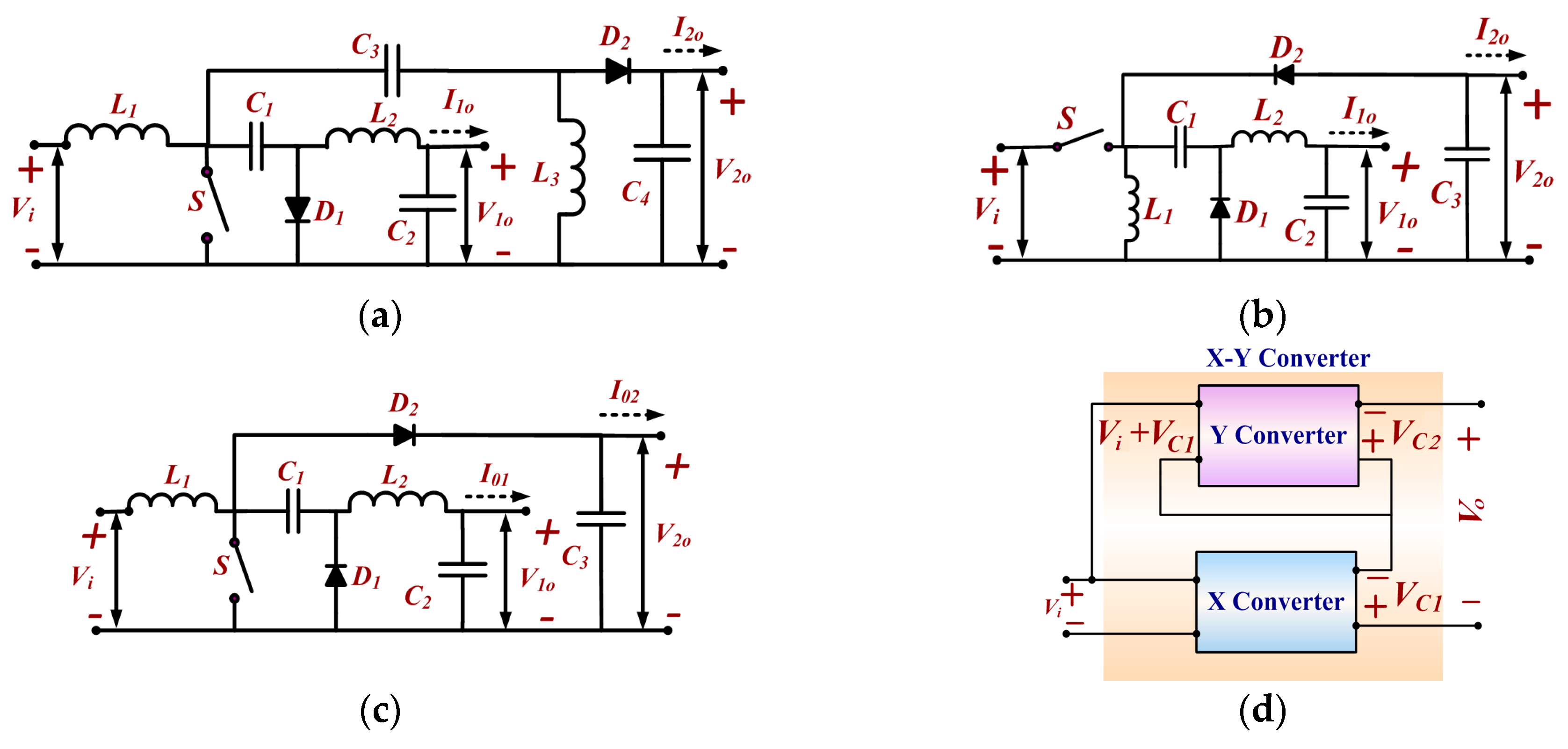
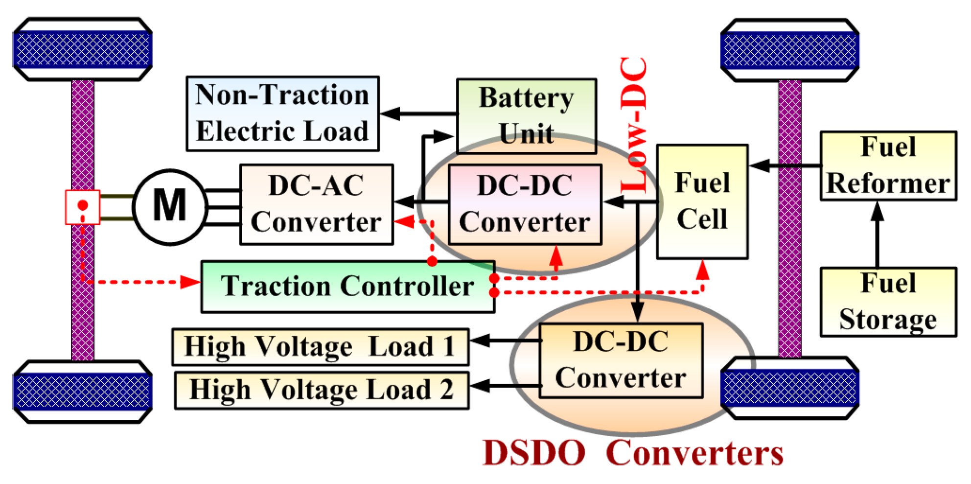
  • The L–Y converters, i.e., an expanded member of the XY converter family that feeds power to two different high voltage loads. At same time, the proposed converter provides high voltage conversion ratio. A diagram of a typical fuel-cell vehicle (FCV) with a DSDO converter is shown Figure 3, where low FC voltage is fed to two high voltage loads.
  • Four new original converter configurations (DSDO L–L, DSDO L-2L, DSDO, L-2LC, and DSDO, L-2LCm) are derived from a single switch.
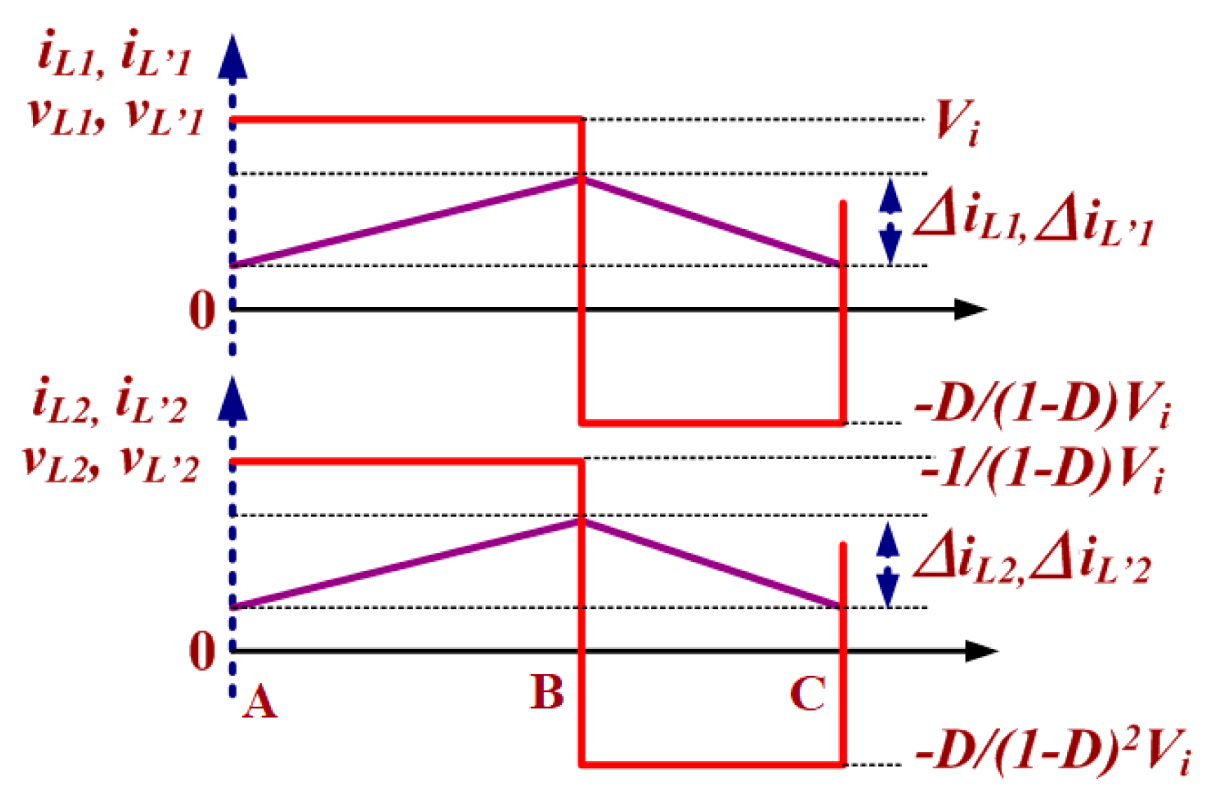
  • The modes of operation, characteristics waveform, and voltage gain analysis for each proposed configuration are discussed in detail.
  • The performance of the proposed converters is validated through numerical simulation and experimental prototype results.

2. Double Stage Double Output Converters

2.1. DSDO L–L Converter

Figure 4 depicts the power circuit of a DSDO L–L converter. In a DSDO L–L converter, a single switch S and input voltage Vi are arranged in two stages. Two L–L converters are employed to obtain dual output voltage. The capacitors C1, C2, inductors L1, L2, and diodes D1, D2, D3 are elements of L–L converter-1. The capacitors C’1, C’2, inductors L’1, L’2, and diodes D’1, D’2, D’3 are elements of L–L converter-2. The stage-1 and stage-1′ voltages are obtained across capacitors C1 and C’1, respectively. The stage-2 and stage-2′ voltages are obtained across capacitors C2 and C’2, respectively. The load R1o is connected across capacitors C1, C2, and load R2o is connected across capacitors C’1 and C’2 to achieve double output voltages, i.e., V1o and V2o, from a single source input (Vi) as shown in Figure 4.
The DSDO L–L converter operates in two modes: switch S turn-ON and another when switch S turn-OFF. Figure 5 shows the characteristics of inductor voltage and current obtained for one switching cycle. Time zone A–B describes the ON time of the switch and time zone B–C describes the OFF time. The equivalent circuit for turn-ON mode is shown in Figure 6a. In this mode, inductor L1 is magnetized through switch S and diode D1 from the input power of voltage Vi. At the same time, input voltage Vi and the voltage across capacitor C1 magnetizes the inductor L2. Total energy stored in capacitors C1 and C2 provide load R1o. Inductor L’1 is magnetized through switch S and diode D’1 by the input voltage Vi. At the same time, input voltage Vi and voltage across capacitor C’1 magnetizes inductor L’2. The energy is delivered to load R2o by capacitors C’1 and C’2. During turn-ON, capacitors C1, C’1, C2, and C’2 are discharged, and inductors L1, L’1, L2, and L’2 are magnetized. Throughout this mode, diodes D1, D’1 are forward biased and diodes D2, D3, D’2, D’3 are reverse biased.
The voltages across inductors can be obtained as follows,
V L 1 = V i ; V L 2 = V C 1 + V i ; V L 1 = V i ; V L 2 = V C 1 + V i
The equivalent circuit for turn-OFF mode is shown in Figure 6b. In this mode, the capacitor C1 is charged by stored energy in the inductor L1 through diode D2. At the same time, capacitor C2 is charged by stored energy in the inductor L2 through diode D3. Energy is provided to load R1o by the connection of inductors L1 and L2. Capacitor C’1 is charged from stored energy in inductor L’1 through diode D’2. At the same time, capacitor C’2 is charged from stored energy in inductor L’2 through diode D’3. Energy is provided to load R2o by connection of inductors L’1 and L’2. In turn-OFF mode, capacitors C1, C’1, C2, and C’2 are charged and inductors L1, L’1, L2, and L’2 are demagnetized. In this mode, diodes D1, D’1 are reverse biased and diodes D2, D3, D’2, and D’3 are forward biased.
The voltages across inductors can be obtained as follows,
V L 1 = V C 1 ; V L 2 = V C 2 ; V L 1 = V C 1 ; V L 2 = V C 2
The output voltages V1o and V2o are obtained as follows,
V C 1 V i = V C 1 V i = D ( 1 D ) 1 , V C 2 V i = V C 2 V i = D ( 1 D ) 2 V 1 o = V 2 o = V i × ( D ( 1 D ) 1 + D ( 1 D ) 2 ) }

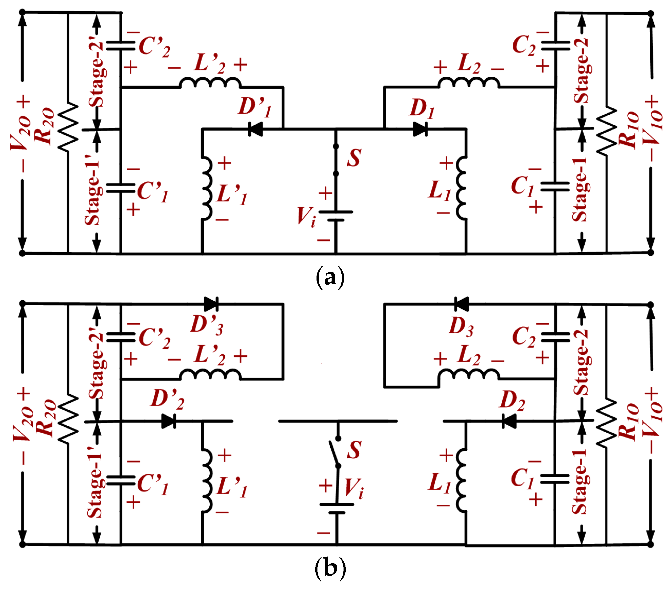
2.2. DSDO L–2L Converter

Figure 7 illustrates the power circuit of a DSDO L–2L converter. A single switch S and input voltage Vi are employed with two-stage L–2L converters to obtain dual output voltage. The capacitors C1, C2 inductors L1, L2, L3, and diodes D1, D2, , and D6 are elements of L–2L converter-1. The capacitors C’1, C’2, inductors L’1, L’2, L’3, and diodes D’1, D’2, , and D’6 are elements of L–2L converter-2. The stage-1 and stage-2 voltages are taken across capacitors C1 and C2, respectively. The stage-1′ and stage-2′ voltages are taken across capacitors C’1 and C’2, respectively. The two output voltages are taken across capacitors C1 + C2 and C’1 + C’2, respectively. The load R1o is connected across capacitors C1 and C2, and load R2o is connected across capacitors C’1 and C’2.
The operation of a DSDO L–2L converter is sectioned into two modes: one when switch S turn-ON and another when switch S turn-OFF. Figure 8 shows the characteristic waveforms of voltage and current of the inductor for one switching cycle. In the characteristic waveform, time zone A–B describes the turn-ON time and time zone B–C describes the turn-OFF time.
The equivalent circuit for turn-ON mode is shown in Figure 9a. Inductor L1 is magnetized by the input voltage Vi. In the same interval, the input voltage Vi and voltage across capacitor C1 magnetizes inductors L2 and L3. Energy is provided to load R1o by capacitors C1 and C2. Inductor L’1 is magnetized by the input voltage Vi. In the same interval, the input voltage Vi and voltage across capacitor C’1 magnetize inductors L’2 and L’3. Energy is provided to load R2o by capacitors C’1 and C’2. During turn-ON mode, capacitors C1, C’1, C2, and C’2 are discharged, and inductors L1, L’1, L2, L’2, L3, and L’3 are magnetized. In this mode, diodes D1, D’1, D3, D’3, D5, and D’5 are forward biased and diodes D2, D’2, D4, D’4, D6, and D’6 are reverse biased.
The voltage across inductors can be obtained as follows,
V L 1 = V L 1 = V i ;   V L 2 = V L 2 = V L 3 = V L 3 = V C 1 + V i
The equivalent circuit of the turn-OFF mode of a DSDO L–2L converter is shown in Figure 9b. In this mode, capacitor C1 is charged by the stored energy of inductor L1. At same time, capacitor C2 is charged by the series connection of inductors L2 and L3. Energy is provided to load R1o by inductors L1, L2, and L3. Capacitor C’1 is charged by the stored energy of inductor L’1, whereas the capacitor C’2 is charged by the series connection of inductors L’2 and L’3. Energy is provided to load R2o by inductors L’1, L’2, and L’3. In turn-OFF mode, capacitors C1, C’1, C2, and C’2 are charged and inductors L1, L’1, L2, L’2, L3, and L’3 are demagnetized. In this mode, diodes D1, D’1, D3, D’3, D5, and D’5 are reverse biased and D2, D’2, D4, D’4, D6, and D’6 are forward biased.
The voltage across inductors can be obtained as follows,
V L 1 = V L 1 = V C 1 ; V L 2 = V L 2 = V L 3 = V L 3 = V C 2 / 2
The output voltages V1o and V2o are obtained as follows,
V C 1 V i = V C 1 V i = D ( 1 D ) 1 , V C 2 V i = V C 2 V i = 2 D ( 1 D ) 2 V 1 o = V 2 o = V i × ( D ( 1 D ) 1 + 2 D ( 1 D ) 2 ) }

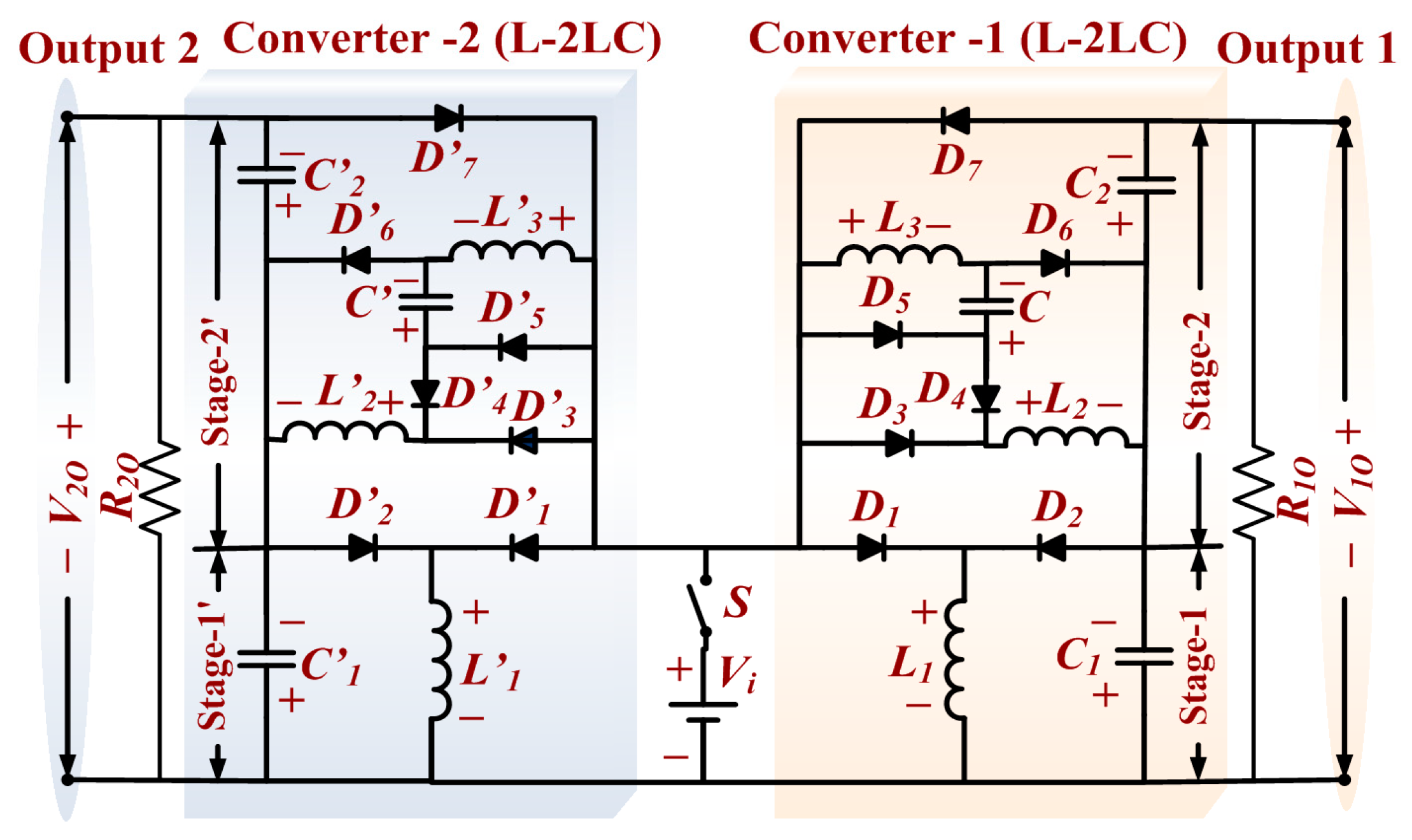
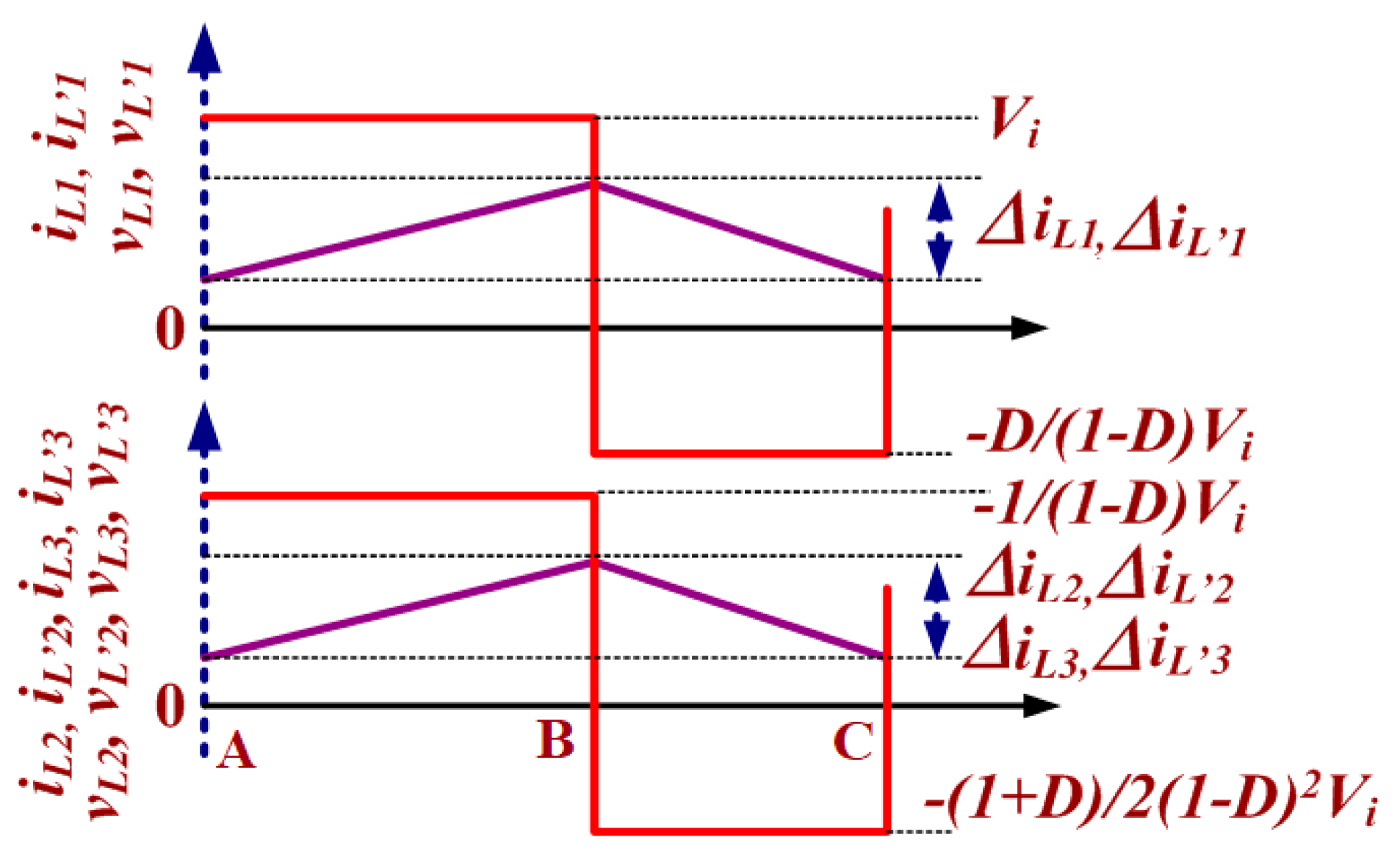
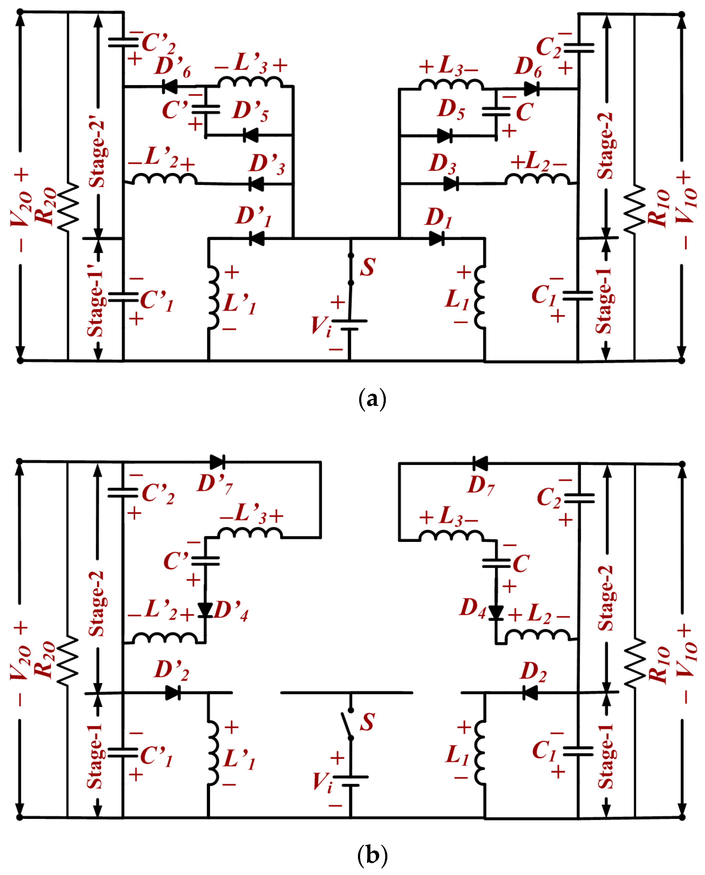
2.3. DSDO L–2LC Converter

Figure 10 illustrates the power circuit of a DSDO L–2LC converter. A single switch S and input voltage Vi are employed with two-stage L–2LC converters to obtain dual output voltages. The capacitors C, C1, and C2, inductors L1, L2, and L3, diodes D1, D2, , and D7 are elements of L–2LC converter-1. The capacitors C’, C’1, and C’2, inductors L’1, L’2, and L’3, diodes D’1, D’2, , and D’7 are elements of L–2LC converter-2. The stage-1 and stage-2 voltages are taken across C1 and C2, respectively. The stage-1′ and stage-2′ voltages are taken across capacitors C’1 and C’2, respectively. The load R1o is connected across capacitors C1 and C2, and load R2o is connected across capacitors C’1 and C’2.
The operation of a DSDO L–2LC converter is sectioned into two modes: one when switch S turn-ON and another when switch S turn-OFF. Figure 11 shows the characteristic waveforms of voltage and current of the inductor for one switching cycle. Time zone A–B describes the turn-ON time and time zone B–C describes the turn-OFF time of the switch. The equivalent circuit for turn-ON mode is shown in Figure 12a. In this interval, inductor L1 is magnetized by the input voltage Vi. The input voltage Vi and voltage across capacitor C1 magnetize inductors L2 and L3, and charge capacitor C in parallel. Energy is provided to load R1o by capacitors C1 and C2. The inductor L’1 magnetized by the input voltage Vi. The input voltage Vi and voltage across capacitor C’1 magnetize inductors L’2 and L’3 and charge the capacitor C’ in parallel. Energy is provided to load R2o by capacitors C’1 and C’2. In turn-ON mode, capacitors C1, C’1, C2, and C’2 are discharged, capacitors C and C’ are charged, and inductors L1, L’1, L2, L’2, L3, and L’3 are magnetized. In this mode, diodes D1, D’1, D3, D’3, D5, D’5, D6, and D’6 are forward biased and diodes D2, D’2, D4, D’4, D7, and D’7 are reverse biased.
The voltages across the inductors are obtained as follows,
V L 1 = V L 1 = V i ;   V L 2 = V L 3 = V L 2 = V L 3 = V C 1 + V i
The equivalent circuit for turn-OFF mode of a DSDO L–2LC converter is shown in Figure 12b. The capacitor C1 is charged by energy stored in inductor L1. The capacitor C2 is charged by the series connection of inductors L2, L3 and capacitor C. Energy is provided to load R1o by inductors L1, L2, L3, and capacitor C. The capacitor C’1 is charged by stored energy of inductor L’1. The capacitor C’2 is charged by the series connection of inductors L’2, L’3, and capacitor C’. Energy is provided to load R2o by inductors L’1, L’2, L’3, and capacitor C’. Hence, the capacitors C1, C’1, C2, and C’2 are charged, capacitors C and C’ are discharged, and inductors L1, L’1, L2, L’2, L3, and L’3 are demagnetized. In this mode, diodes D1, D’1, D3, D’3, D5, D’5, D6, and D’6 are reverse biased and diodes D2, D’2, D4, D’4, D7, and D’7 are forward biased.
The voltages across the inductors can be obtained as follows,
V L 1 = V L 1 = V C 1 ;   ( V L 2 = V L 2 = V L 3 = V L 3 ) = ( V C 2 V C ) 2 = ( V C 2 V C ) 2
The output voltages V1o and V2o are obtained as follows,
V C 1 V i = V C 1 V i = D ( 1 D ) 1 , V C 2 V i = V C 2 V i = ( 1 + D ) ( 1 D ) 2 V 1 o = V 2 o = V i × ( D ( 1 D ) 1 + ( 1 + D ) ( 1 D ) 2 ) }

2.4. DSDO L–2LCm Converter

The DSDO L–2LCm converter is a modified version of the DSDO L–2LC converter, obtained by eliminating two diodes. Figure 13 shows the power circuit of the DSDO L–2LCm converter in which a single switch S and input voltage Vi are employed with two-stage L–2LCm converters to obtain dual output voltages. The capacitors C, C1, and C2, inductors L1, L2, and L3, diodes D1, D2, , and D5 are elements of L–2LCm converter-1. The capacitors C’, C’1, and C’2, inductors L’1, L’2, and L’3, and diodes D’1, D’2, , and D’5 are elements of L–2LCm converter-2. The stage-1 and stage-2 voltages are taken across capacitors C1 and C2, respectively. The stage-1′ and stage-2′ voltages are taken across capacitors C’1 and C’2, respectively. Load R1o is connected across capacitors C1 and C2 and load R2o is connected across capacitors C’1 and C’2.
The operation of a DSDO L–2LCm converter is sectioned into two modes: one when switch S turn-ON and another when switch S turn-OFF. Figure 14 shows the characteristic waveforms of voltage and current for inductors for one switching cycle. The time zone A–B describes the turn-ON time and B–C describes the turn-OFF time. The equivalent circuit for turn-ON mode is shown in Figure 15a. The inductor L1 is magnetized by the input voltage Vi. In the same interval, the inductor Vi and voltage across capacitor C1 magnetize inductors L2 and L3 and charge capacitor C in parallel. The energy is provided to load R1o by capacitors C1 and C2. The inductor L’1 magnetized by the input voltage Vi. In the same interval, input voltage Vi and voltage across capacitor C’1 magnetize inductors L’2 and L’3 and charge capacitor C’ in parallel. The energy is provided to load R2o by capacitors C’1 and C’2. Capacitors C1, C’1, C2, and C’2 are discharged, capacitors C and C’ charged, and inductors L1, L’1, L2, L’2, L3, and L’3 are magnetized. In this mode, diodes D1, D’1, D3, D’3, D4, and D’4 are forward biased and diodes D2, D’2, D5, and D’5 are reverse biased.
The voltages across inductors can be obtained as follows,
V L 1 = V L 1 = V i ;   V L 2 = V L 3 = V L 2 = V L 3 = V C 1 + V i
The equivalent circuit for turn-OFF mode is shown in Figure 15b. Capacitor C1 is charged by the energy of inductor L1, and capacitor C2 is charged by the series connection of inductors L2, L3 and capacitor C. Energy is provided to load R1o by inductors L1, L2, L3, and capacitor C. Capacitor C’1 is charged by energy of inductor L’1. Capacitor C’2 is charged by the series connection of inductors L’2, L’3 and capacitor C’. Energy is provided to load R2o by inductors L’1, L’2, L’3, and capacitor C’. The capacitors C1, C’1, C2, and C’2 are charged, capacitors C and C’ are discharged, and inductors L1, L’1, L2, L’2, L3, and L’3 are demagnetized. Throughout this mode, diodes D1, D’1, D3, D’3, D4, and D’4 are reverse biased, and diodes D2, D’2, D5, and D’5 are forward biased.
The voltages across inductors can be obtained as follows,
V L 1 = V L 1 = V C 1 ; ( V L 2 = V L 2 = V L 3 = V L 3 ) = ( V C 2 V C ) 2 = ( V C 2 V C ) 2
The output voltages V1o and V2o are obtained as follows,
V C 1 V i = V C 1 V i = D ( 1 D ) 1 , V C 2 V i = V C 2 V i = ( 1 + D ) ( 1 D ) 2 V 1 o = V 2 o = V i × ( D ( 1 D ) 1 + ( 1 + D ) ( 1 D ) 2 ) }

3. Comparative Study

In this section, the new DSDO converter configurations are compared with possible parallel combination of conventional converters and recently addressed DC–DC converters. Table 1 tabulates the comparison in terms of number of components and devices, voltage conversion ratio, and ratio of voltage across switch and input voltage. It is observed that one can achieve multiple output voltages by using conventional converters in parallel. However, the voltage conversion ratio is limited and not suitable for feeding high-voltage loads. Hybrid multiple output converters provide two different voltage levels while using common front-end structure. However, the voltage conversion ratio is not significantly improved by using a hybrid structure. The proposed converter provides a higher voltage conversion ratio compared to parallel combination of the conventional converters. In Figure 16a, the voltage conversion ratios of the converters are compared graphically. It is notable that all proposed converters provide inverting high voltage with medium duty cycle. It is observed that the DSDO L–2LC and DSDO L–2LCm converters generate higher voltage conversion ratios compared to the other proposed converters and in comparison to recent DC–DC converters. Figure 16b compares the number of diodes, control switches, inductors, and capacitors. It concludes that the DSDO L–2LCm converter requires fewer diodes than the DSDO L–2LC converter, while both provide the same voltage conversion ratio.

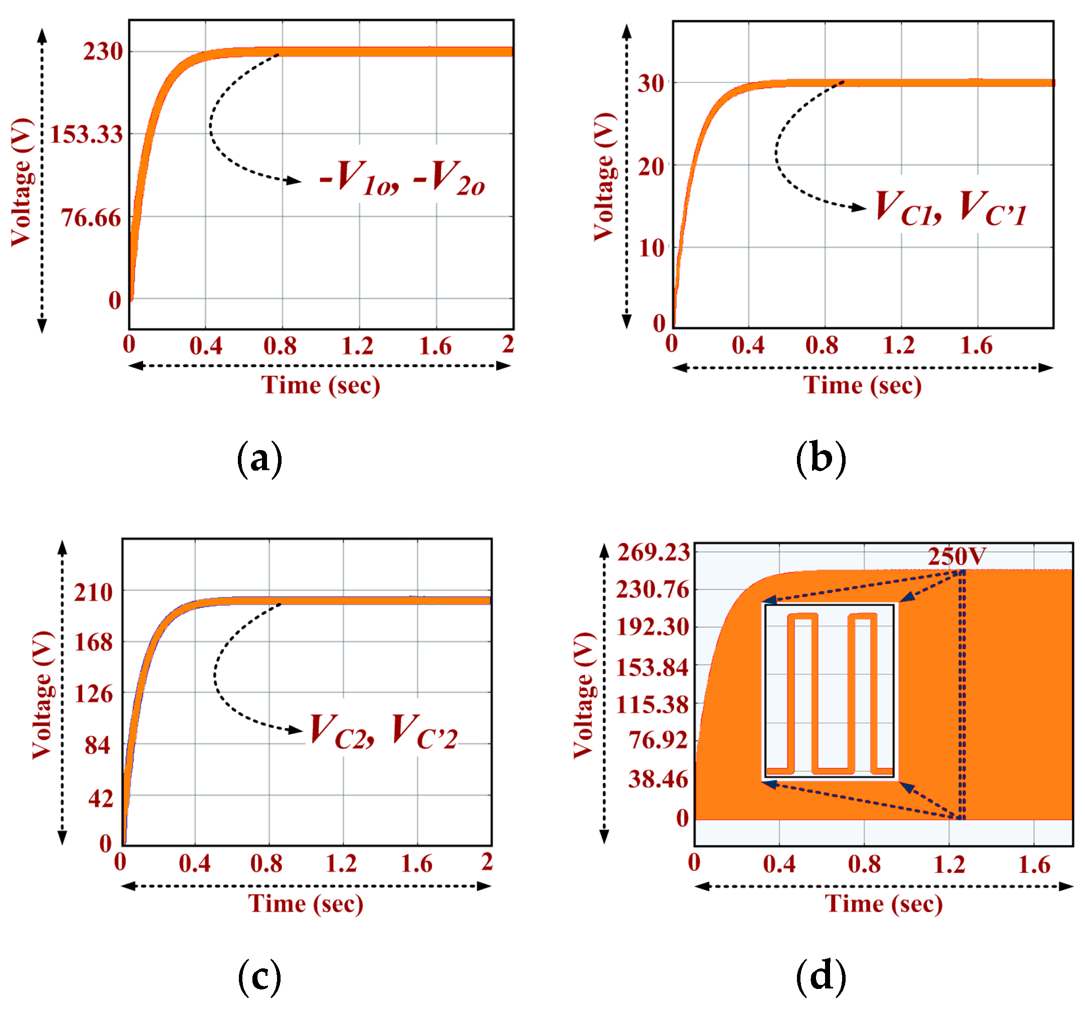
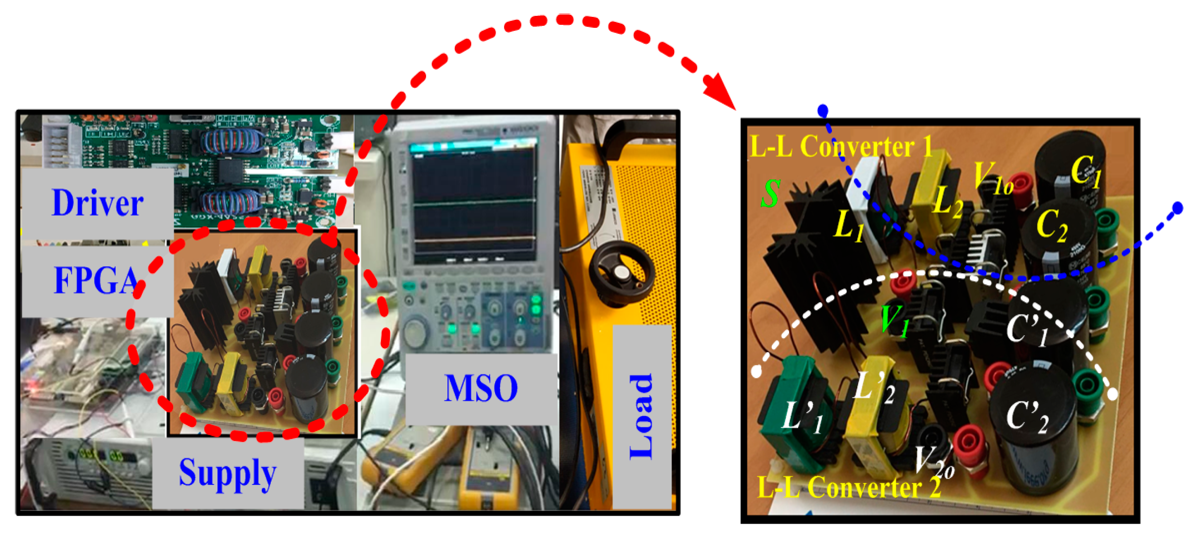
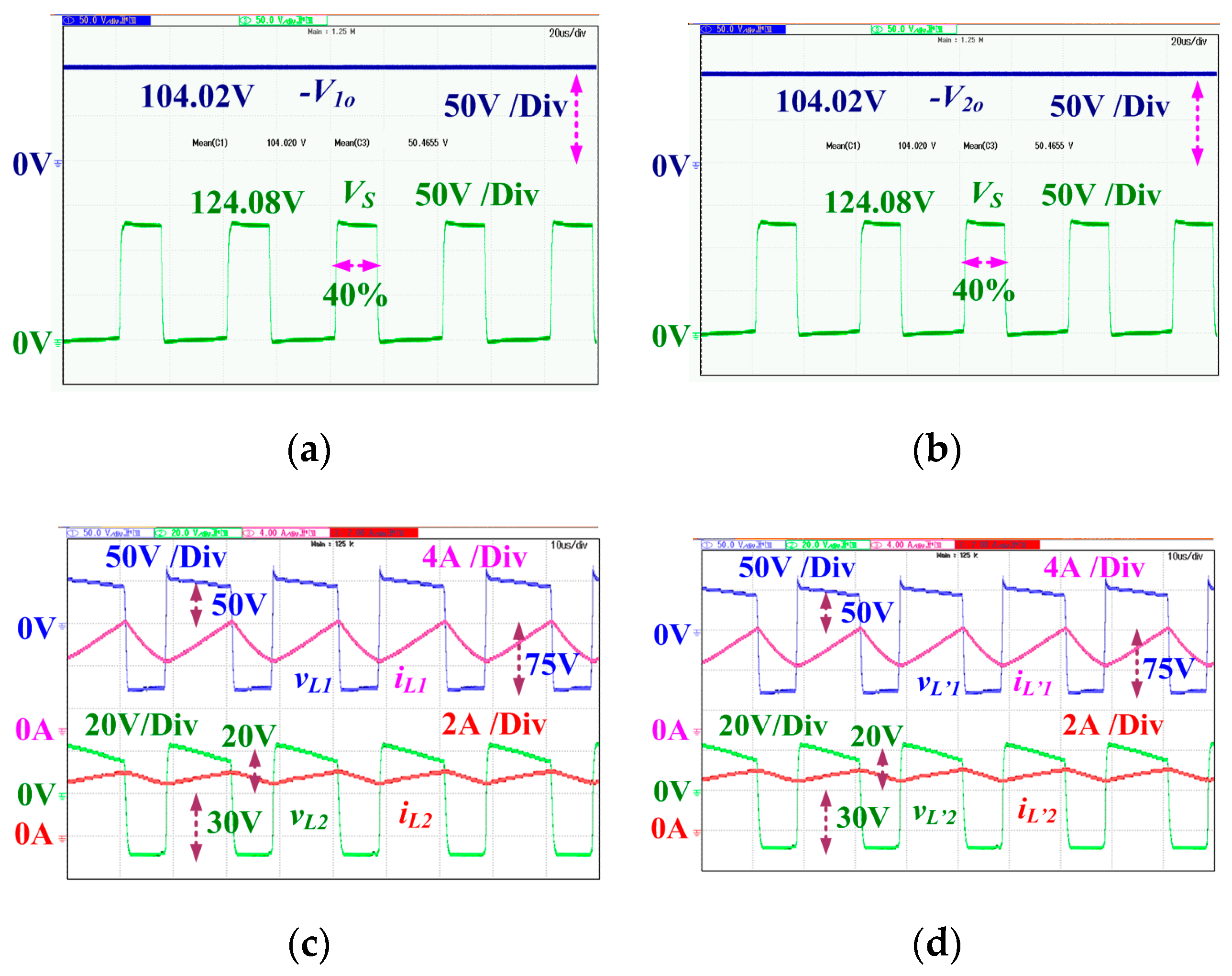
4. Simulation and Experimental Results

The principle and performance of the proposed DSDO converter configurations are validated through numerical simulation software. The converters were designed and tested with two loads, each rated to 100 W with a single input voltage of 20 V and with 25 kHz switching frequency. For simulation and prototype hardware implementation, the values of the reactive components were 220 µF for capacitors and 700 µH for inductors.
DSDO L–L converter: Figure 17a shows the voltage across the two different loads R1o and R2o. Voltage of −105 V was generated across each load with a fixed 60% duty cycle. Figure 17b,c depicts the voltage across capacitors C1, C’1, C2, and C’2. The voltage magnitude across capacitors C1 and C’1 are the same, i.e., 30 V. The voltage magnitudes across capacitors C2 and C’2 are both 75 V. Figure 17d shows that the voltage across switch S of a DSDO L–L converter is 125 V. DSDO L–2L converter: Figure 18a shows the voltage across the two different loads R1o and R2o. Voltage of −180 V was generated across each load with a fixed 60% duty cycle. Figure 18b,c depicts the voltage across capacitors C1, C’1, C2, and C’2, and shows that the voltage magnitude across capacitors C1 and C’1 is 30 V. The voltage magnitudes across capacitors C2 and C’2 are 150 V. Figure 18d shows that the voltage across switch S of the DSDO L–2L converter is 200 V. DSDO L–2LC converter: Figure 19a depicts the voltage across the two different loads R1o and R2o. Voltage of −230 V is generated across each load with a fixed 60% duty cycle. Figure 19b,c shows the waveforms of the voltage across capacitors C1, C’1, C2, and C’2.
The voltage magnitudes across capacitors C1 and C’1 are 30 V and the voltage across capacitors C2 and C’2 are 200 V. Figure 19d shows the voltage across switch S of the DSDO L–2LC converter and its magnitude is 250 V.
DSDO L–2LCm converter: Figure 20a shows the waveforms of the voltage across the two different loads R1o and R2o. Voltage of −230 V is generated across each load with a fixed 60% duty cycle. Figure 20b,c shows the waveforms of the voltage across capacitors C1, C’1, C2, and C’2. The voltage magnitudes across capacitors C1 and C’1 are 30 V, and voltage across capacitors C2 and C’2 are 200 V. Figure 20d shows the voltage across switch S of the DSDO L–2LCm converter and its magnitude is 250 V. Figure 21 shows the preliminary implemented hardware of the DSDO L–L converter. The designed hardware is tested with input voltage of 20 V and the output voltages are controlled at −105 V. Digitally controlled pulses are generated with the help of FPGA (Field Programmable Gate Array). Figure 22a and Figure 22b the voltages across R1o and R2o with the voltage of switch S, respectively. Using a 20 V input supply, −104.2 V is successfully generated across each load and the voltage across switch S is 124.08 V. Figure 22c depicts the voltage and current waveform of inductors L1 and L2, respectively. In the ON state, the voltage across inductor L1 is 20 V, which confirms that inductor L1 is magnetized with input voltage. In the OFF state, the voltage across inductor L1 is −30 V, i.e., inductor L1 is demagnetized to charge the capacitor C1. In the ON state, the voltage across inductor L2 is 50 V, which confirms that the inductor L2 is magnetized by the input voltage and the voltage across capacitor C1. In the OFF state, the voltage across inductor L2 is −75 V, i.e., inductor L2 is demagnetized to charge capacitor C2. Figure 22d depicts the voltage and current waveforms of inductor L’1, L’2 respectively. In the ON state, the voltage across inductor L’1 is 20 V, which confirms that inductor L’1 is magnetized by the input voltage. In the OFF state, the voltage across inductor L’1 is −30 V, i.e., inductor L’1 is demagnetized to charge capacitor C’1. In the ON state, the voltage across inductor L’2 is 50 V, which confirms that inductor L’2 is magnetized by the input voltage and the voltage across capacitor C’1. In the OFF state, the voltage across inductor L’2 is −75 V, i.e., inductor L’2 is demagnetized to charge capacitor C’2.

5. Conclusions

This article developed four DSDO converter configurations for high voltage fuel-cell electric vehicular loads. The proposed converters need a single controlling semiconductor switch and are able to feed two loads with high voltage conversion ratio. The circuitry of the DSDO L–L, DSDO L–2L, DSDO L–2LC, and DSDO L–2LCm converters are developed by merging with two L–L, two L–2L, two L–2LC, and two L–2LCm converters, respectively. The operating principles of the proposed converters are discussed with detailed theoretical analysis and governing equations for the output voltage conversion ratio. Finally, it is concluded that among the proposed converters, the DSDO L–2LC and DSDO L–2LCm converters provide higher output voltage and are effective in comparison with DC–DC converters. Both simulation and experimental results show that the proposed DSDO L–L converters had the expected performance.

Author Contributions

All authors contributed equally for the research work, to present the final manuscript as full research article in current version.

Funding

This research received no external funding.

Conflicts of Interest

The authors declare no conflict of interest.

References

  1. Rezaee, S.; Farjah, E. A DC–DC Multiport Module for Integrating Plug-In Electric Vehicles in a Parking Lot: Topology and Operation. IEEE Trans. Power Electron 2014, 29, 5688–5695. [Google Scholar] [CrossRef]
  2. Mercorelli, P.; Kubasiak, N.; Liu, S. Model predictive control of an electromagnetic actuator fed by multilevel PWM inverter. In Proceedings of the IEEE International Symposium on Industrial Electronics, Ajaccio, France, 4–7 May 2004; pp. 531–535. [Google Scholar]
  3. Mercorelli, P.; Kubasiak, N.; Liu, S. Multilevel bridge governor by using model predictive control in wavelet packets for tracking trajectories. In Proceedings of the IEEE International Conference on Robotics and Automation, New Orleans, LA, USA, 26 April–1 May 2004; pp. 4079–4084. [Google Scholar]
  4. Faraji, R.; Adib, E.; Farzanehfard, H. Soft-switched non-isolated high step-up multi-port DC-DC converter for hybrid energy system with minimum number of switches. Intl. J. Electr. Power Energy Sys. 2019, 106, 511–519. [Google Scholar] [CrossRef]
  5. Mercorelli, P. A Multilevel Inverter Bridge Control Structure with Energy Storage Using Model Predictive Control for Flat Systems. J. Eng. 2019, 1–15. [Google Scholar] [CrossRef]
  6. Kubasiak, N.; Mercorelli, P.; Liu, S. Model Predictive Control of Transistor Pulse Converter for Feeding Electromagnetic Valve Actuator with Energy Storage. In Proceedings of the IEEE 44th Conference on Decision and Control, Seville, Spain, 12–15 December 2005; pp. 6794–6799. [Google Scholar]
  7. Lucia, U. Overview on fuel cells. Renew. Sustain. Energy Rev. 2014, 30, 164–169. [Google Scholar] [CrossRef]
  8. Peighambardoust, S.J.; Rowshanzamir, S.; Amjadi, M. Review of the proton exchange membranes for fuel cell applications. Intl. J. Hydrog. Energy 2010, 35, 9349–9384. [Google Scholar] [CrossRef]
  9. Zhang, Z.; Pittini, R.; Andersen, M.A.E.; Thomsena, O.C. A Review and Design of Power Electronics Converters for Fuel Cell Hybrid System Applications. Energy Procedia 2012, 20, 301–310. [Google Scholar] [CrossRef] [Green Version]
  10. Cheng, S.; Lo, Y.; Chiu, H.; Kuo, S. High-Efficiency Digital-Controlled Interleaved Power Converter for High-Power PEM Fuel-Cell Applications. IEEE Trans. Ind. Electron. 2013, 60, 773–780. [Google Scholar] [CrossRef]
  11. Bhaskar, M.S.; Al-ammari, R.; Mohammad, M.; Padmanaban, S.; Iqbal, A. A New Triple-Switch-Triple-Mode High Step-Up Converter with Wide Range of Duty Cycle for DC Microgrid Applications. IEEE Trans. Ind. Appl. 2019, 1. [Google Scholar] [CrossRef]
  12. Maroti, P.K.; Al-Ammari, R.; Bhaskar, M.S.; Meraj, M.; Iqbal, A.; Padmanaban, S.; Rahman, S. New tri-switching state non-isolated high gain DC–DC boost converter for microgrid application. IET Power Electron 2019, 12, 2741–2750. [Google Scholar] [CrossRef]
  13. Yang, L.; Liang, T.; Chen, J. Transformerless DC–DC Converters with High Step-Up Voltage Gain. IEEE Trans. Ind. Electron. 2009, 56, 3144–3152. [Google Scholar] [CrossRef]
  14. Bhaskar, M.S.; Meraj, M.; Iqbal, A.; Padmanaban, S.; Maroti, P.K.; Alammari, R. High Gain Transformer-Less Double-Duty-Triple-Mode DC/DC Converter for DC Microgrid. IEEE Access 2019, 7, 36353–36370. [Google Scholar] [CrossRef]
  15. Muranda, C.; Ozsoy, E.; Padmanaban, S.; Bhaskar, M.S.; Fedak, V.; Ramachandaramurthy, V.K. Modified SEPIC DC-to-DC boost converter with high output-gain configuration for renewable applications. In Proceedings of the IEEE Conference on Energy Conversion CENCON’17, Kuala Lumpur, Malaysia, 30–31 October 2017; pp. 317–322. [Google Scholar]
  16. Oluwafemi, A.W.; Ozsoy, E.; Padmanaban, S.; Bhaskar, M.S.; Ramachandaramurthy, V.K.; Fedak, V. A modified high output-gain cuk converter circuit configuration for renewable applications—A comprehensive investigation. In Proceedings of the IEEE Conference on Energy Conversion CENCON’17, Kuala Lumpur, Malaysia, 30–31 October 2017; pp. 117–122. [Google Scholar]
  17. Morales-Saldana, A.; Gutierrez, E.E.C.; Leyva-Ramos, J. Modeling of switch-mode dc-dc cascade converters. IEEE Trans. Aerosp. Electron. Syst. 2002, 38, 295–299. [Google Scholar] [CrossRef]
  18. Bhaskar, M.S.; Padmanaban, S.; Blaabjerg, F.; Wheeler, P.W. An Improved Multistage Switched Inductor Boost Converter (Improved M-SIBC) for Renewable Energy Applications: A key to Enhance Conversion Ratio. In Proceedings of the IEEE 19th Workshop on Control and Modeling for Power Electronics COMPEL’18, Padua, Italy, 25–28 June 2018. [Google Scholar]
  19. De Novaes, Y.R.; Rufer, A.; Barbi, I. A New Quadratic, Three-Level, DC/DC Converter Suitable for Fuel Cell Applications. In Proceedings of the IEEE Power Conversion Conference-Nagoya, Nagoya, Japan, 2–5 April 2007; pp. 601–607. [Google Scholar]
  20. Iqbal, A.; Bhaskar, M.S.; Meraj, M.; Padmanaban, S. DC-Transformer Modelling, Analysis and Comparison of the Experimental Investigation of a Non-Inverting and Non-Isolated Nx Multilevel Boost Converter (Nx MBC) for Low to High DC Voltage Applications. IEEE Access 2018, 6, 70935–70951. [Google Scholar] [CrossRef]
  21. Iqbal, A.; Bhaskar, M.S.; Meraj, M.; Padmanaban, S.; Rahman, S. Closed-Loop Control and Boundary for CCM and DCM of Non-Isolated Inverting Nx Multilevel Boost Converter for High Voltage Step-Up Applications. IEEE Trans. Ind. Electron. 2019, 1. [Google Scholar] [CrossRef]
  22. Bhaskar, M.S.; Padmanaban, S.; Blaabjerg, F. A Multistage DC-DC Step-Up Self-Balanced and Magnetic Component-Free Converter for Photovoltaic Applications: Hardware Implementation. Energies 2017, 10, 719. [Google Scholar] [CrossRef]
  23. Ranjana, M.S.B.; Alammari, R.; Meraj, M.; Iqbal, A.; Padmanaban, S. Modified Multilevel Buck-Boost Converter with Equal Voltage across Each Capacitor: Analysis and Experimental Investigations. IET Power Electron. 2019. [Google Scholar] [CrossRef]
  24. Bhaskar, M.S.; Meraj, M.; Iqbal, A.; Padmanaban, S. Non-isolated Symmetrical Interleaved Multilevel Boost Converter with Reduction in Voltage Rating of Capacitors for High Voltage Microgrid Applications. IEEE Trans. Ind. Appl. 2019, 1. [Google Scholar] [CrossRef]
  25. Tahan, M.; Bamgboje, D.; Hu, T. Flyback-Based Multiple Output dc-dc Converter with Independent Voltage Regulation. In Proceedings of the 9th IEEE International Symposium on Power Electronics for Distributed Generation Systems, PEDG, Charlotte, NC, USA, 25–28 June 2018; pp. 1–8. [Google Scholar]
  26. Wai, R.J.; Liaw, J.J. High-Efficiency-Isolated Single-Input Multiple-Output Bidirectional Converter. IEEE Trans. Power Electron. 2015, 30, 4914–4930. [Google Scholar] [CrossRef]
  27. Kim, J.K.; Choi, S.W.; Kim, C.E.; Moon, G.W. A New Standby Structure Using Multi-Output Full-Bridge Converter Integrating Flyback Converter. IEEE Trans. Ind. Electron. 2011, 58, 4763–4767. [Google Scholar] [CrossRef]
  28. Ferrera, M.; Litrán, S.; Aranda, E.; Márquez, J.A. A Converter for Bipolar DC Link Based on SEPIC-Cuk Combination. IEEE Trans. Power Electron. 2015, 30, 6483–6487. [Google Scholar] [CrossRef]
  29. Durán, E.; Litrán, S.P.; Ferrera, M.B.; Andújar, J.M. A Zeta-Buck-Boost converter combination for Single-Input Multiple-Output applications. In Proceedings of the 42nd Annual Conference of the IEEE Industrial Electronics Society, Florence, Italy, 23–26 October 2016; pp. 1251–1256. [Google Scholar]
  30. Pires, V.F.; Foito, D.; Baptista, F.B.; Silva, J. A photovoltaic generator system with a DC/DC converter based on an integrated Boost-Ćuk topology. Sol. Energy 2016, 136, 1–9. [Google Scholar] [CrossRef]
  31. Liu, X.; Xu, J.; Chen, Z.; Wang, N. Single-Inductor Dual-Output Buck-Boost Power Factor Correction Converter. IEEE Trans. Ind. Electron. 2015, 62, 943–952. [Google Scholar] [CrossRef]
  32. Sanjeevikumar, P.; Bhaskar, M.S.; Dhond, P.; Blaabjerg, F.; Pecht, M. Non-isolated Sextuple Output Hybrid Triad Converter Configurations for High Step-Up Renewable Energy Applications. In Power Systems and Energy Management; Springer: Berlin/Heidelberg, Germany, 2018; pp. 1–12. [Google Scholar]
  33. Patra, P.; Patra, A.; Misra, N. A Single-Inductor Multiple-Output Switcher with Simultaneous Buck, Boost, and Inverted Outputs. IEEE Trans. Power Electron. 2011, 27, 1936–1951. [Google Scholar] [CrossRef]
  34. Bhaskar, M.S.; Padmanaban, S.; Kulkarni, R.; Blaabjerg, F.; Seshagiri, S.; Hajizadeh, A. Novel LY converter topologies for high gain transfer ratio: A new breed of XY family. In Proceedings of the 4th IET Clean Energy and Technology Conference, IET-CEAT, Kuala Lumpur, Malaysia, 14–15 November 2016; pp. 1–8. [Google Scholar]
  35. Mahajan, S.B.; Sanjeevikumar, P.; Wheeler, P.; Blaabjerg, F.; Rivera, M.; Kulkarni, R. X-Y converter family: A new breed of buck boost converter for high step-up renewable energy applications. In Proceedings of the IEEE International Conference on Automatica IEEE-ICA-ACCA, Curico, Chile, 19–21 October 2016; pp. 1–8. [Google Scholar]
  36. Bhaskar, M.S.; Sanjeevikumar, P.; Iqbal, A.; Meraj, M.; Howeldar, A.; Kamuruzzaman, J. L-L Converter for Fuel Cell Vehicular Power Train Applications: Hardware Implementation of Primary Member of X-Y Converter Family. In Proceedings of the IEEE Power Electronics, Drives and Energy Systems PEDES’18, Chennai, India, 18–21 December 2018. [Google Scholar]
  37. Maroti, P.K.; Padmanaban, S.; Bhaskar, M.S.; Blaabjerg, F.; Ramachandaramurthy, K.V.; Siano, P.; Fedak, V. A novel 2L-Y DC-DC converter topologies for high conversion ratio renewable application. In Proceedings of the IEEE Conference on Energy Conversion CENCON’17, Kuala Lumpur, Malaysia, 30 October 2017; pp. 323–328. [Google Scholar]
  38. Padmanaban, S.; Bhaskar, M.S.; Blaabjerg, F.; Yang, Y. A New DC-DC Multilevel Breed of XY Converter Family for Renewable Energy Applications: LY Multilevel Structured Boost Converter. In Proceedings of the 44th Annual Conference of the IEEE Industrial Electronics Society, Washington, DC, USA, 21–23 October 2018; pp. 6110–6115. [Google Scholar]
Figure 1. Power circuit of conventional parallel converters: (a) boost-boost converter; (b) buck-boost-buck-boost converter; (c) Cuk-Cuk converter; (d) single ended primary inductance converter (SEPIC)-SEPIC converter; (e) ZETA-ZETA converter; (f) boost-boost converter with common front-end structure; (g) buck-boost-buck-boost converter with common front end structure; (h) Cuk-Cuk converter with common front-end structure; (i) SEPIC-SEPIC converter with common front-end structure; (j) ZETA-ZETA converter with common front-end structure.
Energies 12 03681 g001aEnergies 12 03681 g001b
Figure 2. Power circuit of (a) SEPIC-Cuk converter, (b) ZETA–Buck-boost converter, (c) boost-Cuk converter; (d) Basic block diagram of the X–Y converter family.
Energies 12 03681 g002
Figure 3. Typical structure of fuel cell (FC) vehicle with double stage double output (DSDO) converters.
Energies 12 03681 g003
Figure 4. Power circuit of a DSDO L–L converter.
Energies 12 03681 g004
Figure 5. Waveforms of inductor voltages and currents for a DSDO L–L converter.
Energies 12 03681 g005
Figure 6. Equivalent circuitry of a DSDO L–L converter: (a) ON mode; (b) OFF mode.
Energies 12 03681 g006
Figure 7. Power circuit of a DSDO L–2L converter.
Energies 12 03681 g007
Figure 8. Waveforms of inductor voltage and current for a DSDO L–2L converter.
Energies 12 03681 g008
Figure 9. Equivalent circuitry of a DSDO L–2L converter: (a) ON mode; (b) OFF mode.
Energies 12 03681 g009
Figure 10. Power circuit of a DSDO L–2LC converter.
Energies 12 03681 g010
Figure 11. Waveforms of inductor voltage and current for a DSDO L–2LC converter.
Energies 12 03681 g011
Figure 12. Equivalent circuitry of DSDO L–2LC converter: (a) ON mode; (b) OFF mode.
Energies 12 03681 g012
Figure 13. Power circuit of the DSDO L–2LCm converter.
Energies 12 03681 g013
Figure 14. Waveforms of inductor voltage and current for a DSDO L–2LCm converter.
Energies 12 03681 g014
Figure 15. Equivalent circuitry of a DSDO L–2LCm converter: (a) ON mode; (b) OFF mode.
Energies 12 03681 g015
Figure 16. Comparison of (a) voltage conversion ratio versus duty cycle and (b) number of diodes (Nd), number of capacitors (NC), number of Switches (NS), and number of inductors (NL). A: Boost, B: SEPIC, C: Cuk or Buck-Boost, D: DSDO L–L, E: DSDO L–2L, F: DSDO L–2LC, G: DSDO L–2LCm converters.
Energies 12 03681 g016
Figure 17. Simulation results of the DSDO L–L converter configuration: (a) Output voltages waveforms; (b) Voltage waveforms across stage-1 and stage-2; (c) Voltage waveforms across stage-1′ and stage-2′; (d) Voltage waveform across switch S.
Energies 12 03681 g017
Figure 18. Simulation results of the DSDO L–2L converter configuration: (a) Output voltages waveforms; (b) Voltage waveforms at stage-1 and stage-2; (c) Voltage waveforms at stage-1′ and stage-2′; (d) Voltage waveform across switch S.
Energies 12 03681 g018
Figure 19. Simulation results of the DSDO L–2LC converter configuration: (a) Output voltages waveforms; (b) Voltage waveforms across stage-1 and Stage-2; (c) Voltage waveforms across stage-1′ and stage-2′; (d) Voltage across switch S.
Energies 12 03681 g019
Figure 20. Simulation results of the DSDO L–2LCm converter configuration: (a) Output voltages waveforms; (b) Voltage waveforms across stage-1 and Stage-2; (c) Voltage waveforms across stage-1′ and stage-2′; (d) Voltage across switch S.
Energies 12 03681 g020
Figure 21. Experimental setup of the DSDO L–L converter configuration.
Energies 12 03681 g021
Figure 22. Experimental results of the DSDO L–L converter configuration: (a) voltage at load R1o and voltage across switch S waveforms; (b) voltage at load R2o and voltage across switch S waveforms; (c) inductor voltages and current of L converter-1; and (d) inductor voltages and current of L converter-2.
Energies 12 03681 g022
Table 1. Comparison of Converters.
ConverterSwitchesInductorsDiodesCapacitorsVoltage Conversion Ratio (V1o,V2o)Voltage Stress across Switch (Vs/Vi)
Converter without common front-end structure
Boost-Boost converter (Figure 1a)22221/1-D, 1/1-D1/1-D
Buck-Boost-Buck-Boost converter (Figure 1b)2222-D/1-D, -D/1-D1/1-D
Cuk-Cuk Converter (Figure 1c)2424-D/1-D, -D/1-D1/1-D
SEPIC-SEPIC Converter (Figure 1d)2424D/1-D, D/1-D1/1-D
ZETA-ZETA Converter (Figure 1e)2424D/1-D, D/1-D1/1-D
Converter with common front-end structure
Boost-Boost converter (Figure 1f)11221/1-D, 1/1-D1/1-D
Buck-Boost-Buck-Boost converter (Figure 1g)1122-D/1-D, -D/1-D1/1-D
Cuk-Cuk converter (Figure 1h)1324-D/1-D, -D/1-D1/1-D
SEPIC-SEPIC converter (Figure 1i)1324D/1-D, D/1-D1/1-D
ZETA-ZETA converter (Figure 1j)1324D/1-D, D/1-D1/1-D
Hybrid multi-output converter with common front-end structure
SEPIC-Cuk converter (Figure 2a)1324-D/1-D, D/1-D1/1-D
ZETA–Buck-boost converter (Figure 2b)1223D/1-D, -D/1-D1/1-D
Boost-Cuk converter (Figure 2c)1223-D/1-D, 1/1-D1/1-D
Proposed DSDO converter configurations
DSDO L–L converters (Figure 4)1464D(1-D)−1 + D(1-D)−21+ D(1-D)−1 + D(1-D)−2
DSDO L–2L converters (Figure 7)16124D(1-D)−1 + 2D(1-D)−21+ D(1-D)−1 + 2D(1-D)−2
DSDO L–2LC converters (Figure 10)16146D(1-D)−1 + (1 + D)(1-D)−21+ D(1-D)−1 + (1 + D)(1-D)−2
DSDO L–2LCm converters (Figure 13)16106D(1-D)−1 + (1 + D)(1-D)−21+ D(1-D)−1 + (1 + D)(1-D)−2

