Article

Parameter Analysis and Optimization of Class-E Power Amplifier Used in Wireless Power Transfer System

1
School of Automation, Nanjing University of Science and Technology, Nanjing 210094, China
2
Jiangsu Provincial Key Laboratory of Smart Grid Technology and Equipment, Nanjing 210096, China
*
Author to whom correspondence should be addressed.
Energies 2019, 12(17), 3240; https://doi.org/10.3390/en12173240
Submission received: 18 July 2019 / Revised: 11 August 2019 / Accepted: 20 August 2019 / Published: 22 August 2019
(This article belongs to the Special Issue Modelling of Wireless Power Transfer)

Abstract

:
In this paper, a steady-state matrix analysis method is introduced to analyze the output characteristics of the class-E power amplifier used in a wireless power transfer (WPT) system, which takes the inductance resistance, on-resistance and leakage current of metal-oxide-semiconductor field effect transistor (MOSFET) into account so that the results can be closer to the actual value. On this basis, the parameters of the class-E power amplifier are optimized, and the output power is improved under the premise of keeping the efficiency unchanged. Finally, the output characteristics of the amplifier before and after optimization are compared by an experiment, while the B-field strength around the WPT system is studied through simulation. The experimental results verify the correctness and feasibility of the optimization method based on steady-state matrix analysis.

1. Introduction

The Class-E power amplifier is widely used in high-frequency power supply, wireless power transfer (WPT) and other fields because of its simple structure and high output efficiency [1,2]. In 2007, the research team of Massachusetts Institute of Technology (MIT) put forward the magnetic coupling resonant wireless power transfer technology, and the class-E power amplifier has once again become a hot research topic at home and abroad [3].
MOSFET can meet the zero-voltage switching (ZVS) and zero-derivative switching (ZDS) conditions when the class-E power amplifier works under the ideal condition and the efficiency is 100% [4]. According to the parametric characters of the class-E power amplifier, the authors studied the changes in output characteristics of class-E power amplifiers when the load deviated from the optimal value in [5]. The relationship between the DC power supply of a class-E power amplifier and MOSFET’s peaks voltage is studied in [6]. The effect of various parameters of a class-E power amplifier on the output characteristics of the circuit, the voltage and the current waveform of the MOSFET are analyzed in [7]. T. Mury and his team conducted an in-depth study on the operating characteristics of class-E power amplifiers in the sub-optimal working state where the duty cycle of the MOSFET is not 50%, the mathematical modeling of the class-E power amplifier is carried out, and the influence of duty cycle on the current peak, output voltage and current is analyzed [8]. The analysis of a class-E power amplifier based on a lossless switch and ratio-frequency (RF) choke (RFC) was introduced in [9]. In [10] and [11], researchers used resonant soft-switching converters to achieve optimum switching conditions. Class-EF inverters and the equations of the voltages and currents were derived with traditional analysis in [12]. In [13], a novel topology of the Class-EM power amplifier was proposed based on a finite direct current (DC)-feed inductance and an isolation circuit. R. A. Beltran et al., proposed a simplified analysis and design of class-E outphasing transmitters that predicts efficiency and output power as a function of input drive phase difference based on classic design equations of the class-E amplifier [14]. However, the analytical processes of the traditional class-E power amplifier circuit above are ideal, generally ignoring the MOSFET’s turn-on resistance and considering the turn-off resistance to be infinite. In other words, analysis of every component in load network is based on the complete ideal condition such as no impedance [15]. There is a certain difference between the theoretical result and the actual value where the performance of the class-E power amplifier can be significantly influenced by the non-ideal factor such as the inductance resistance, finite dc-feed inductance, leakage current and so on [16].
In this paper, a steady-state matrix analysis method which proved to be a fast and effective approach for optimization of switching-mode power amplifiers [17,18,19,20] is used for studying the output characteristics of two kinds of class-E power amplifiers (a traditional choke, RFC type [21], parallel load type, parallel capacitor and inductor (PCL) type [22]) under the consideration of non-ideal factors, such as the inductance resistance, leakage current and so on. On the basis of inductance of phase angle compensation Lx (Lin), the influence of the parallel resonant capacity Cp and the load RL on the output power, the operation efficiency and the maximum withstand voltage of MOSFET is turned off, two kinds of class-E power amplifiers are optimized. The output power of the class-E power amplifier is improved on ensuring output efficiency and the effectiveness of optimization of class-E power amplifier circuit based on steady-state matrix analysis is verified according to the experiments. The B-field strength around the WPT system is also simulated and studied.

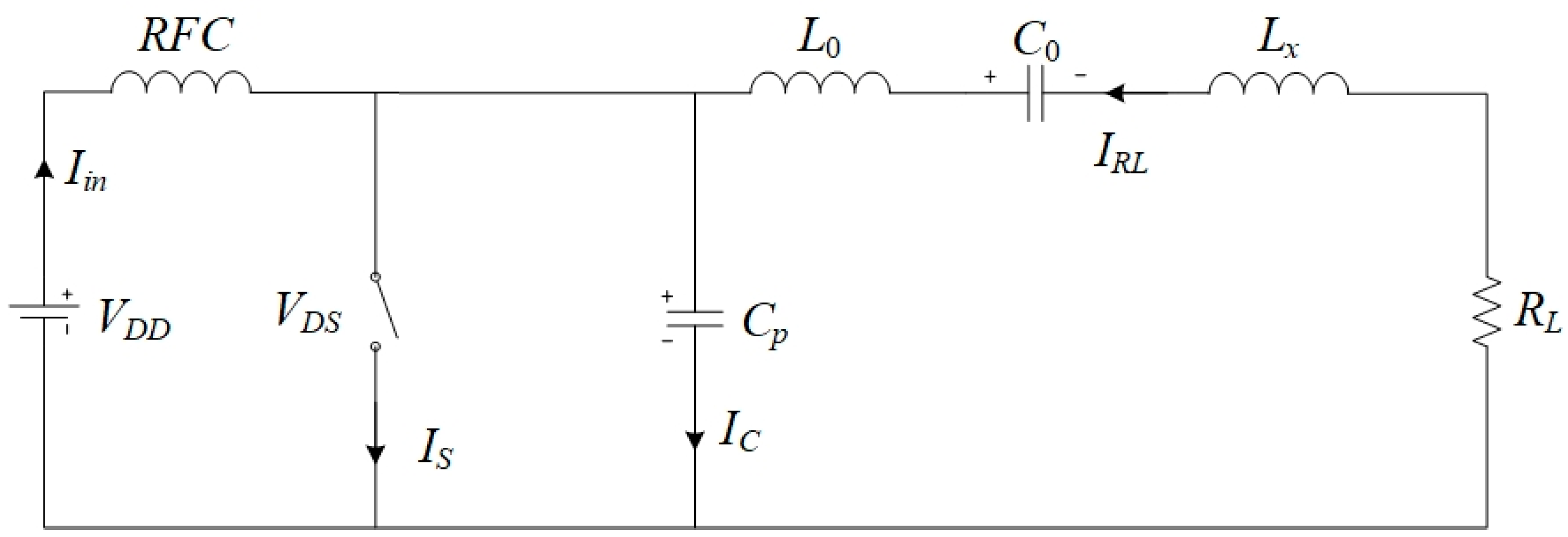
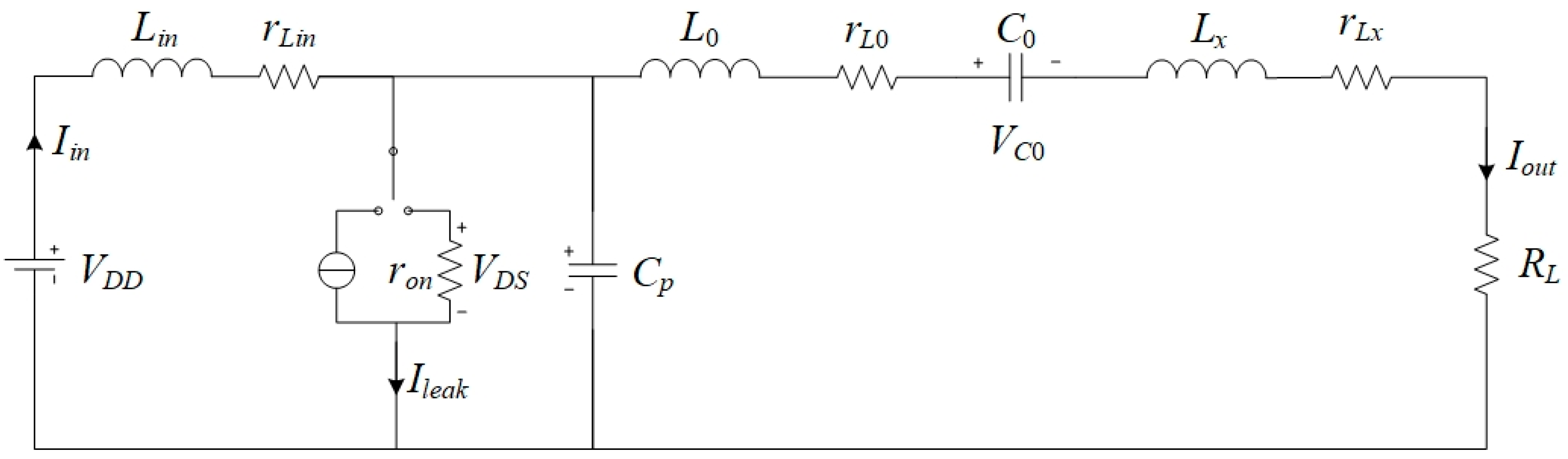
2. Application of Steady-State Matrix Analysis Method

The equivalent circuit of the traditional class-E power amplifier is shown in Figure 1.
The average value of the voltage on the MOSFET during one period is equal to the DC power supply, VDD:
V D D = 1 2 π 0 2 π V D S ( ω t ) d ω t = π I i n ω C P
In the ideal case, the efficiency of the Class-E power amplifier is 100%, where the active power absorbed by the load is equal to the input provided by the DC power supply:
I i n V D D = I R L 2 2 R L
P o = 0.5768 V D D 2 R L
The voltage applied to RL and Lx is the fundamental frequency voltage, which can be obtained by Fourier analysis:
{ V R = 1 π 0 2 π V D S ( ω t ) sin ( ω t ) d ω t V L x = 1 π 0 2 π V D S ( ω t ) cos ( ω t ) d ω t
The parameter calculation formula of the class-E power amplifier load network can be derived from (4):
ω L x R L = 1.1525
ω C P R L = 0.1836
The maximum withstand voltage on the MOSFET is:
V d s _ max = 3.562 V D D
MOSFET’s turn-on resistance, leakage current and inductance resistance in the load network are considered in the circuit diagram of a class-E power amplifier in Figure 2. MOSFET’s loss can be divided into the on-resistance loss and the leakage current loss in turn-off state. Inductance resistance comes from choke (parallel inductor) Lin resonant inductor L0 and inductance of phase angle compensation Lx.
The state variables in the diagram is defined as the following matrix:
q ( t ) = [ I i n ( t ) I o u t ( t ) V D S ( t ) V C O ( t ) ] T ,
Iin(t) is the input current of DC power supply, Iout(t) is the output current, VDS(t) is drain-source voltage, VC0(t) is the voltage of the resonant capacitor. They are energy storage variables in the circuit, Therefore, the switching state of the MOSFET will not cause changes immediately, which meets the requirement of steady-state analysis.
The state equation of class-E power amplifier circuit can be obtained by the first derivative of the state variable. When MOSFET is turned off, the equation of state is:
{ L i n d I i n ( t ) d t = V D D V D S ( t ) r L i n I i n ( t ) ( L 0 + L x ) d I o u t ( t ) d t = V D S ( t ) ( r L 0 + r L x + R L ) I o u t ( t ) V C 0 ( t ) C p d V D S ( t ) d t = I i n ( t ) I o u t ( t ) I l e a k C O d V C O ( t ) d t = I o u t ( t ) .
Changing Ileak to VDS/ron in (9), the equation of state when MOSFET is turned on is obtained. All the equations of state have the form of first-order differential equations:
d q ( t ) d t = A q ( t ) + B .
The state of matrix A and matrix B have different forms when the MOSFET is turned off and turned on. For the convenience of analysis, the state matrix when MOSFET is turned off is defined as A1 and B1, the off-time is t1. Moreover, the state matrix when MOSFET is turned on is defined as A2 and B2, and the on-time is t2. The solution of (10) is:
q ( t ) = e A t q 0 + 0 t e A ( t τ ) B d τ = e A t q 0 + A 1 ( e A t I ) B ,
q0 is the initial value. The solution of the state equation is:
q 1 ( t ) = e A 1 t q 01 + A 1 1 ( e A 1 t I ) B 1 ,
q 2 ( t ) = e A 2 t q 02 + A 2 1 ( e A 2 t I ) B 2 .
Because of the energy properties of the state variable, there is no immediate change of state variable when MOSFET works from turn-off to turn-on. As the MOSFET is turned off, the state variable at t1 time is equal to the value at t = 0 that is q01. The following equations can be derived:
q 02 = q 1 ( t 1 ) = e A 1 t 1 q 01 + A 1 1 ( e A 1 t 1 I ) B 1 ,
q 01 = q 2 ( t 2 ) = e A 2 t 2 q 02 + A 2 1 ( e A 2 t 2 I ) B 2 .
The initial value q01, q02 can be obtained in (14) and (15), losses and output power can be defined:
W 1 = 0 t 1 q 1 q 1 T d t ,
W 2 = 0 t 2 q 2 q 2 T d t .
Output power:
P O U T = R L T 0 T I O U T 2 ( t ) d t = R L T { W 1 [ 2 , 2 ] + W 2 [ 2 , 2 ] } .
Loss of the inductor resistance:
P r L 0 = r L 0 T { W 1 [ 2 , 2 ] + W 2 [ 2 , 2 ] } ,
P r L X = r L X T { W 1 [ 2 , 2 ] + W 2 [ 2 , 2 ] } ,
P r L i n = r L i n T { W 1 [ 1 , 1 ] + W 2 [ 1 , 1 ] } .
Loss of MOSFET in turn-on and turn-off state are shown as follows:
P S o n = 1 T C o n ( 0 t 2 q 2 q 2 T d t ) C o n T ,
P S o f f = 1 T C o f f ( 0 t 1 q 1 d t ) C o f f T ,
C o n = [ 0 0 1 / R o n 0 ] ,
C o f f = [ 0 0 I l e a k 0 ] .
The output power of class-E power amplifier, efficiency and drain-source voltage of MOSFET can be obtained according to (16)–(25).

3. Analysis of the Characteristic of Class-E Power Amplifier

Based on the steady-state matrix analysis method above, the effect of the inductor phase angle compensation Lx (Lin) and parallel capacitance Cp on the output characteristics of two kinds of class-E power amplifier can be studied. The theoretical parameter values of two types with a DC power supply of 25 V, working at 6 MHz and output power of 30 W are shown in Table 1. RL-og, LX_og, L0_og, and C0_og are theoretical values of load resistance, inductance of phase angle compensation, inductance and capacitance of resonant circuit. Lin_og and Cp_og are theoretical values of choke (parallel) inductance and capacitance. rLX, rLin, and rL0 are resistance values of the inductors.
In order to analyze the effect of Lx (Lin) and Cp on the output characteristics of class-E power amplifier, the surface graph of its parametric characters is obtained based on the steady-state matrix method. In the following analysis, MRF6V2150NBR1 is used so that MOSFET’s turn-on resistance Ron is 0.3 Ω, the leakage current Ileak is 2.5 mA, and drain source maximum withstand voltage is 110 V.

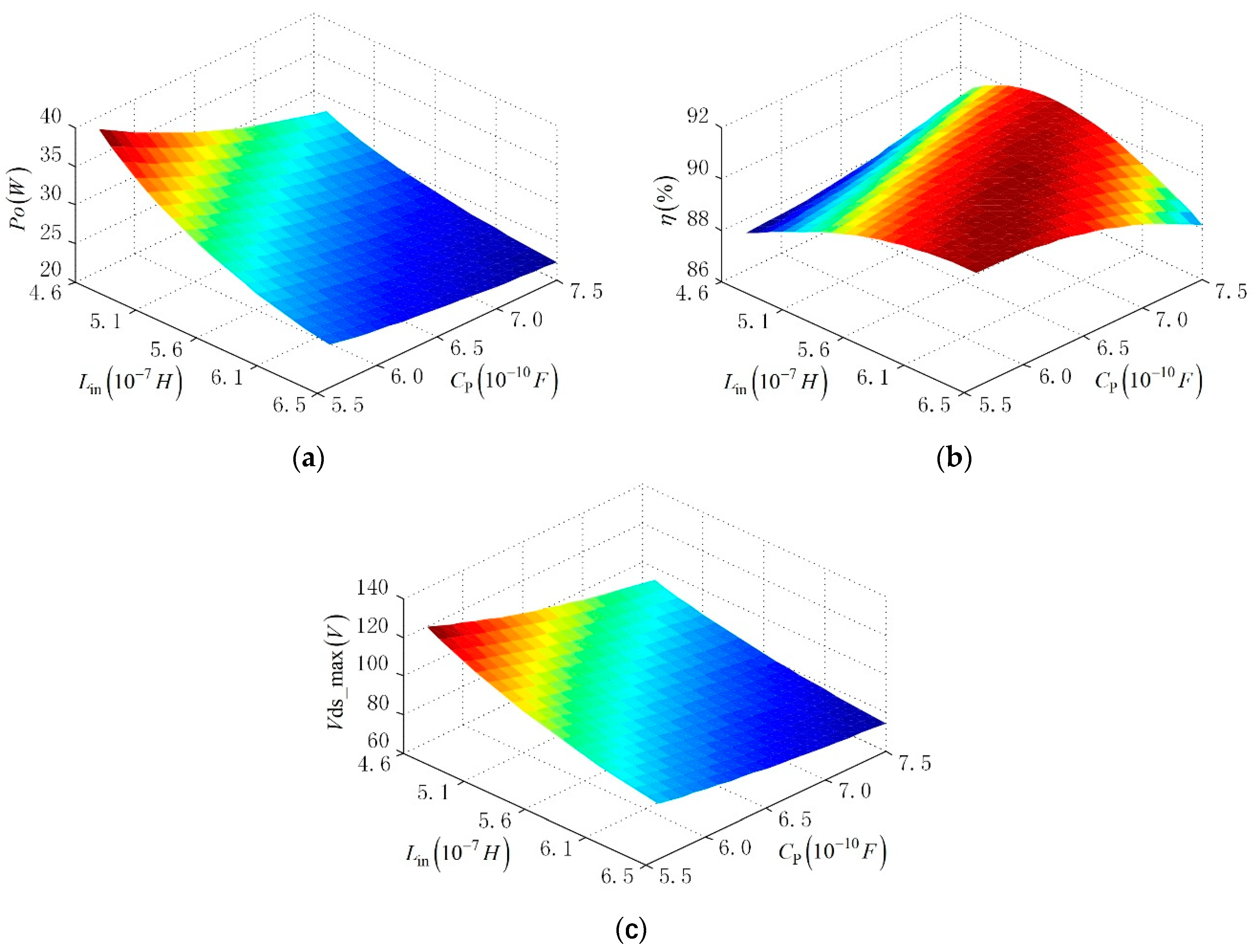
3.1. Influence of RFC Output Characteristics

The effect of phase angle compensation inductance Lx which is parallel with capacitance Cp and the load RL on output power, efficiency and MOSFET’s peak voltage in RFC type is shown in Figure 3 and Figure 4. The variation range of Lx is from 0.27 μH to 0.47 μH, Cp is from 300 pF to 500 pF and RL is from 8 Ω to 16 Ω. If MOSFET’s peaks voltage exceeds the maximum withstand voltage, it will cause damage to MOSFET. Therefore, the maximum withstand voltage should also be considered in designing a class-E power amplifier.
With the increase of Lx and Cp, the output power of the RFC type decreases significantly, the efficiency increases firstly and then decreases. The trend of output efficiency is opposite to the trend of output power, and the influence of the two factors should be considered comprehensively in the design of circuit parameters. Moreover, Lx has little effect on the maximum voltage of MOSFET, and its value decreases mainly with the increase of Cp, which can be obtained from Figure 3.
It can be seen from Figure 4 that the output power of the class-E power amplifier decreases while the efficiency increases with the increase of RL. The effect of load RL on output power is obvious, while the trend of the output efficiency is opposite to that of the output power. On the other hand, Lx has less influence on the maximum voltage of MOSFET than RL. However, within the variation range, the voltage peak across the MOSFET is smaller than its maximum value, ensuring that the MOSFET can work normally without being broken down.

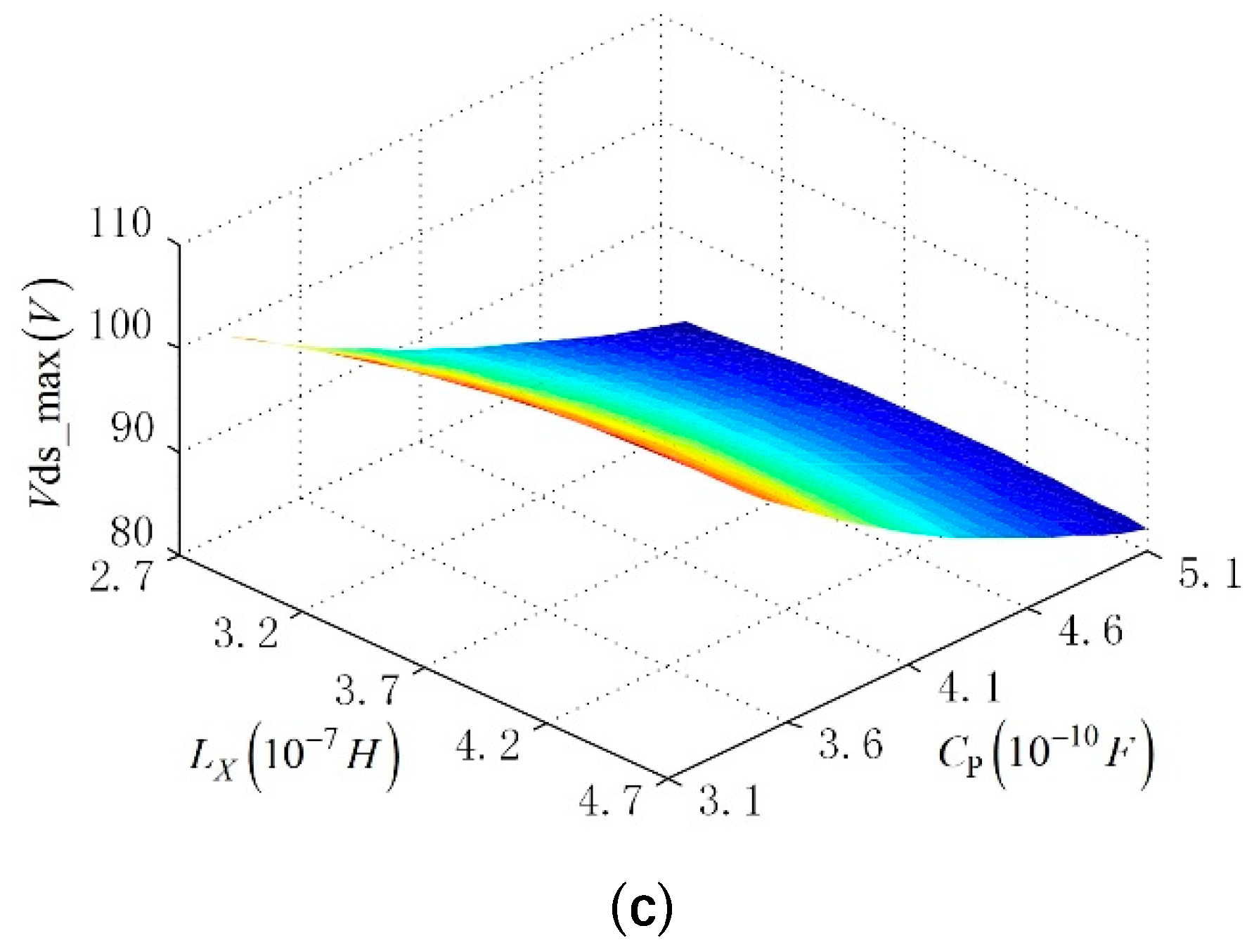
3.2. Influence of PCL Characteristics

The effect of phase angle compensation inductance Lin on output power, efficiency and MOSFET peaks voltage in PCL type is shown in Figure 5. The variation range of Lin is from 0.45 μH to 0.65 μH, Cp is from 550 pF to 750 pF.
With the increase of Lin and Cp, the output power of the PCL type also decreases as shown in Figure 5a; when the Cp value is fixed, the efficiency increases firstly and then decreases with the increase of Lin, when the Lin value is small, the efficiency increases with the increase of Cp, while the Lin value becomes larger, the efficiency gradually turns to decrease with the increase of Cp as shown in Figure 5b; the maximum withstand voltage of PCL type decreases significantly with the increase of Lin and Cp as shown in Figure 5c. When the Lin and Cp values are too small, the maximum withstand voltage will exceed 120 V, which will easily cause damage to the MOSFET.

3.3. Optimization Strategy of Two Kinds of Class-E Power Amplifier

According to the analysis above, due to the existence of inductance resistance and non-ideal MOSFET, the designed circuit parameters are no longer optimal under ideal condition. The model of class-E power amplifiers using state equations is closer to the real situation. For the design of a broadband class-E power amplifier, if the reactance corresponding to the phase shifting inductor Lx is regarded as part of the load impedance, the circuit can be optimized overall by adjusting the phase shifting inductor Lx (Lin), Cp and RL under the condition of working at 6 MHz and output power of 30 W.
The RFC type parameters before and after optimization are shown in Table 2. The ideal values are calculated according to (1)–(7). As we select Lx = 0.34 μH, Cp = 0.38 nF, RL = 9.12 Ω according to Figure 3 and Figure 4, the output efficiency of the optimized class-E power amplifier has no obvious change, the output power is increased by 9.25% (2.6 W). Moreover, the maximum withstand voltage of MOSFET is slightly increased in turn-off stage.
The PCL type parameters before and after optimization are shown in Table 3. Select Lin = 0.54 μH, Cp = 0.6 nF. Under the condition that the output efficiency of the optimized class-E power amplifier has no obvious change, the output power is increased by 7.61% (2.02 W). Moreover, the maximum withstand voltage of MOSFET in turn-off stage is increased significantly, still within the safe range.

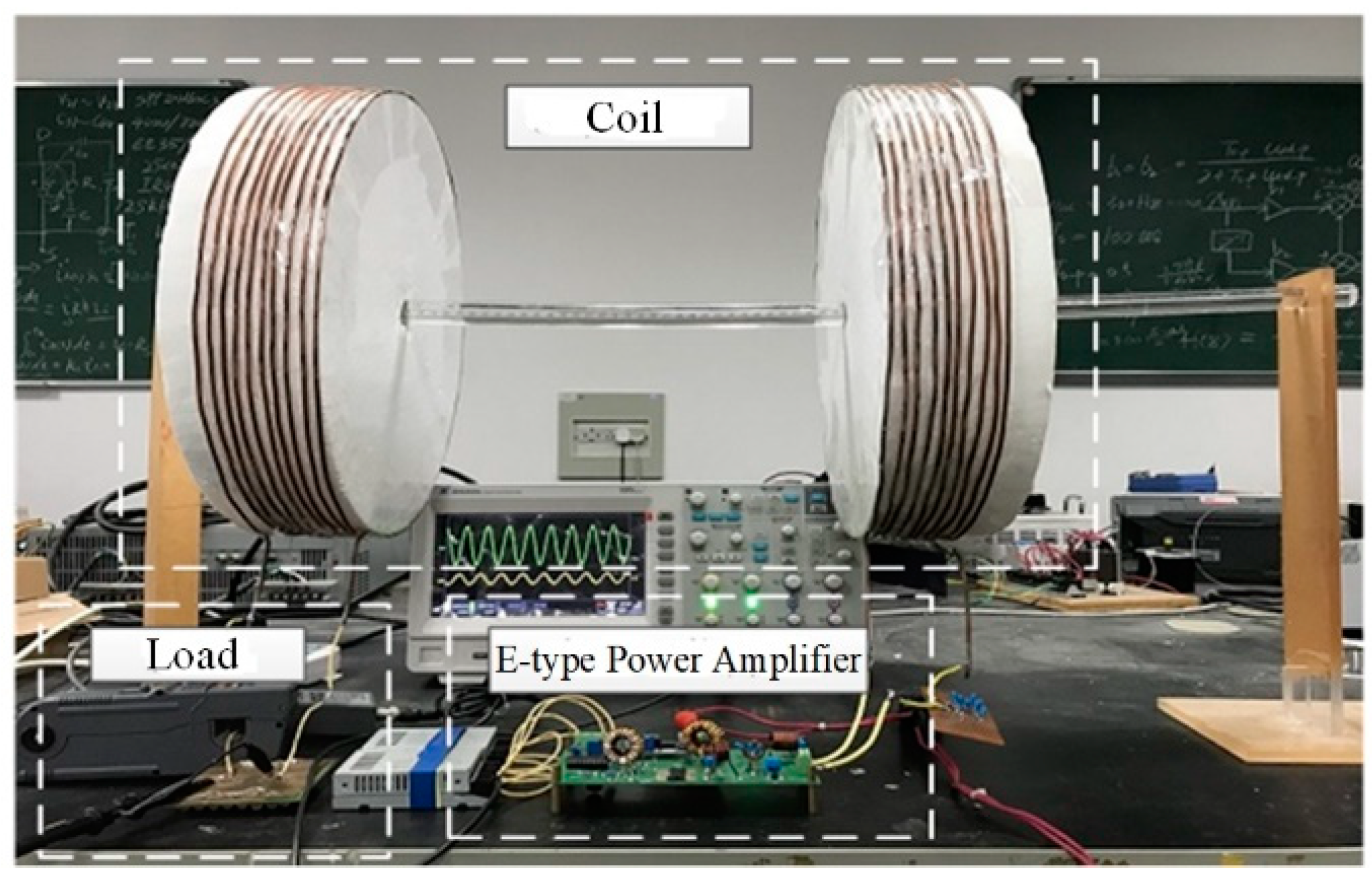
4. Experimental Results and Analysis

Comparing the output character of two kinds of class-E power amplifier before and after optimization, the validity of the optimization method is verified using the parameters obtained from the analysis. The experimental platform is built as shown in Figure 6.

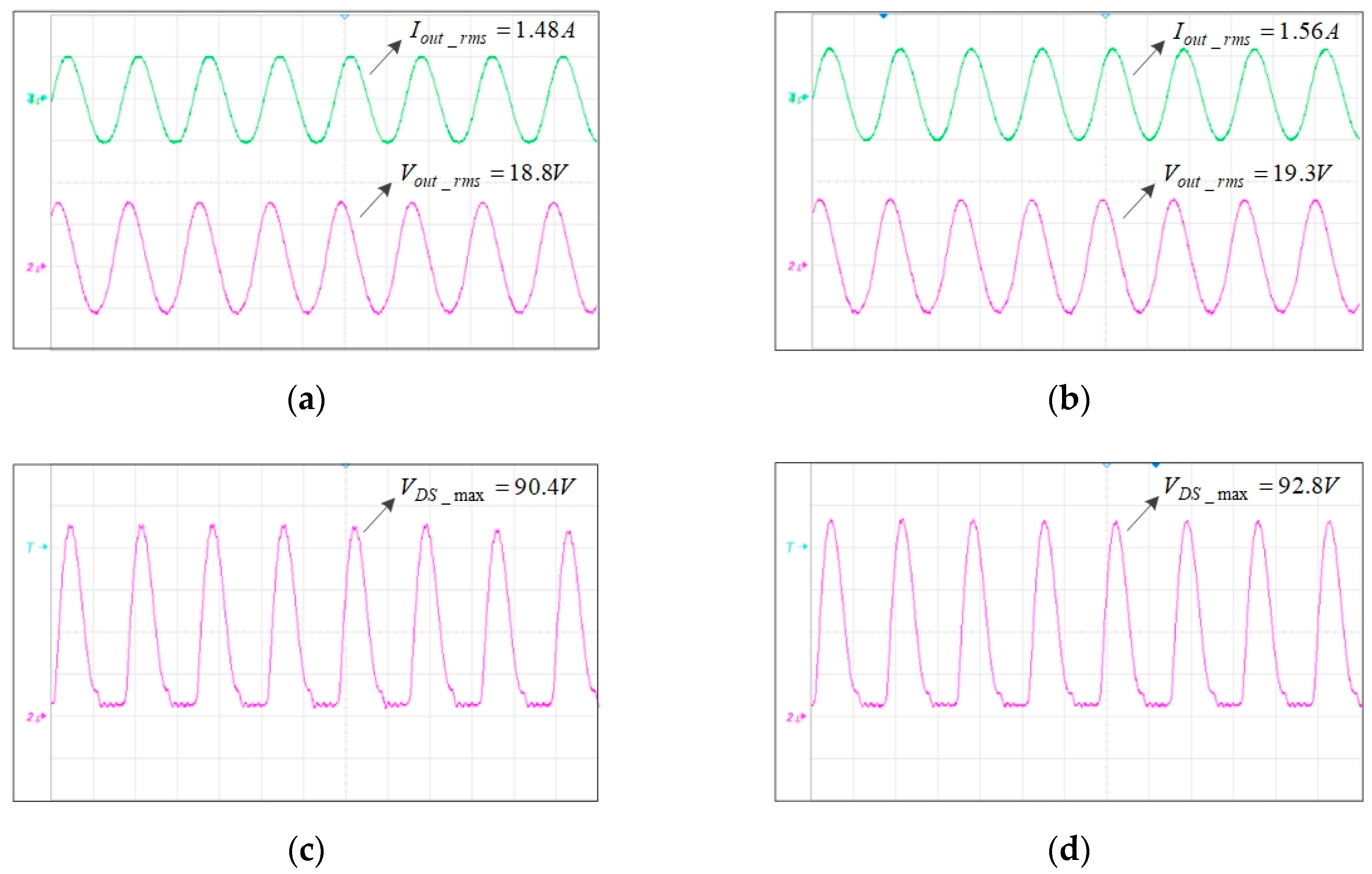
4.1. Experiments of RFC Type under Non-Ideal Condition

The experimental waveforms of RFC type before and after optimization is shown in Figure 7. Before optimization, the RMS of the output current, the output voltage and the output power of RFC type were 1.48 A, 18.8 V and 27.82 W. The operational efficiency was 85.24%. After optimization, the RMS of the output current, the output voltage and the output power became 1.56 A, 19.3 V and 30.11 W. The operational efficiency was 84.76%.
Under the condition that the efficiency has no obvious change, the output power is increased by 2.29 W (8.23%).
The maximum withstand voltage of MOSFET in turn-off stage increases from 90.4 V to 92.8 V, which is still within the safe range. Moreover, due to the small voltage oscillation in turn-on stage which increases the loss of the MOSFET, the experimental output efficiency is smaller than the theoretical value.

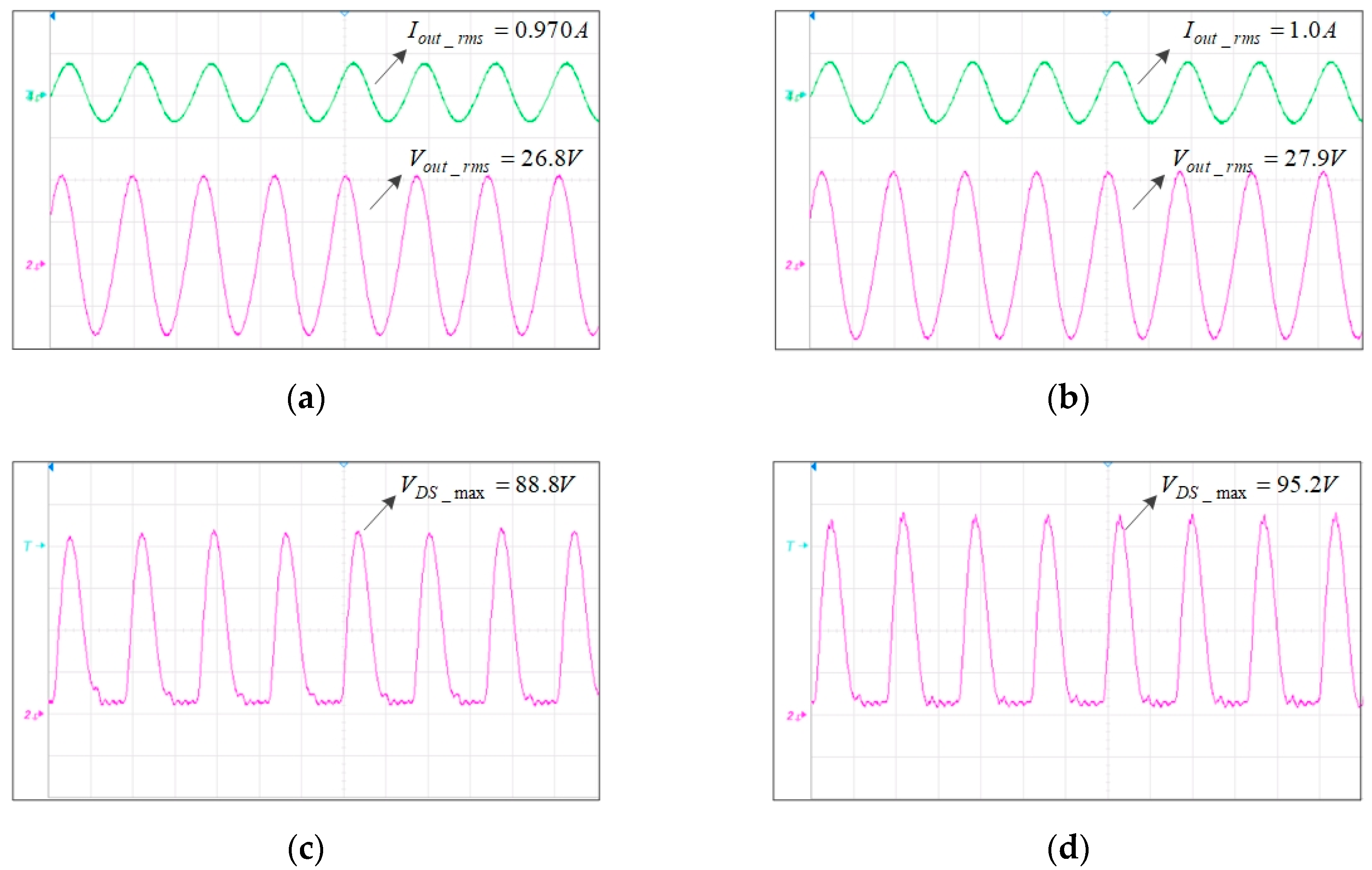
4.2. Experiments of PCL Type under Non-Ideal Condition

The experimental waveforms of PCL type before and after optimization are shown in Figure 8. Before optimization, the RMS of the output current of PCL type was 0.97 A, the output voltage was 26.8 V and the output power was 25.99 W; the efficiency was 85.57%. After optimization, the RMS of the output current of RFC type was 1.0 A, the output voltage was 27.9 V, and the output power was 27.90 W; the efficiency was 85.84%. Under the condition that the output efficiency had no obvious change, the output power increased by 1.91 W (7.35%). The maximum withstand voltage of MOSFET was increased from 88.8 V to 95.2 V, but still within the safe range.

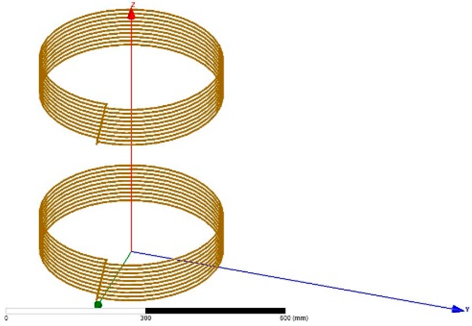
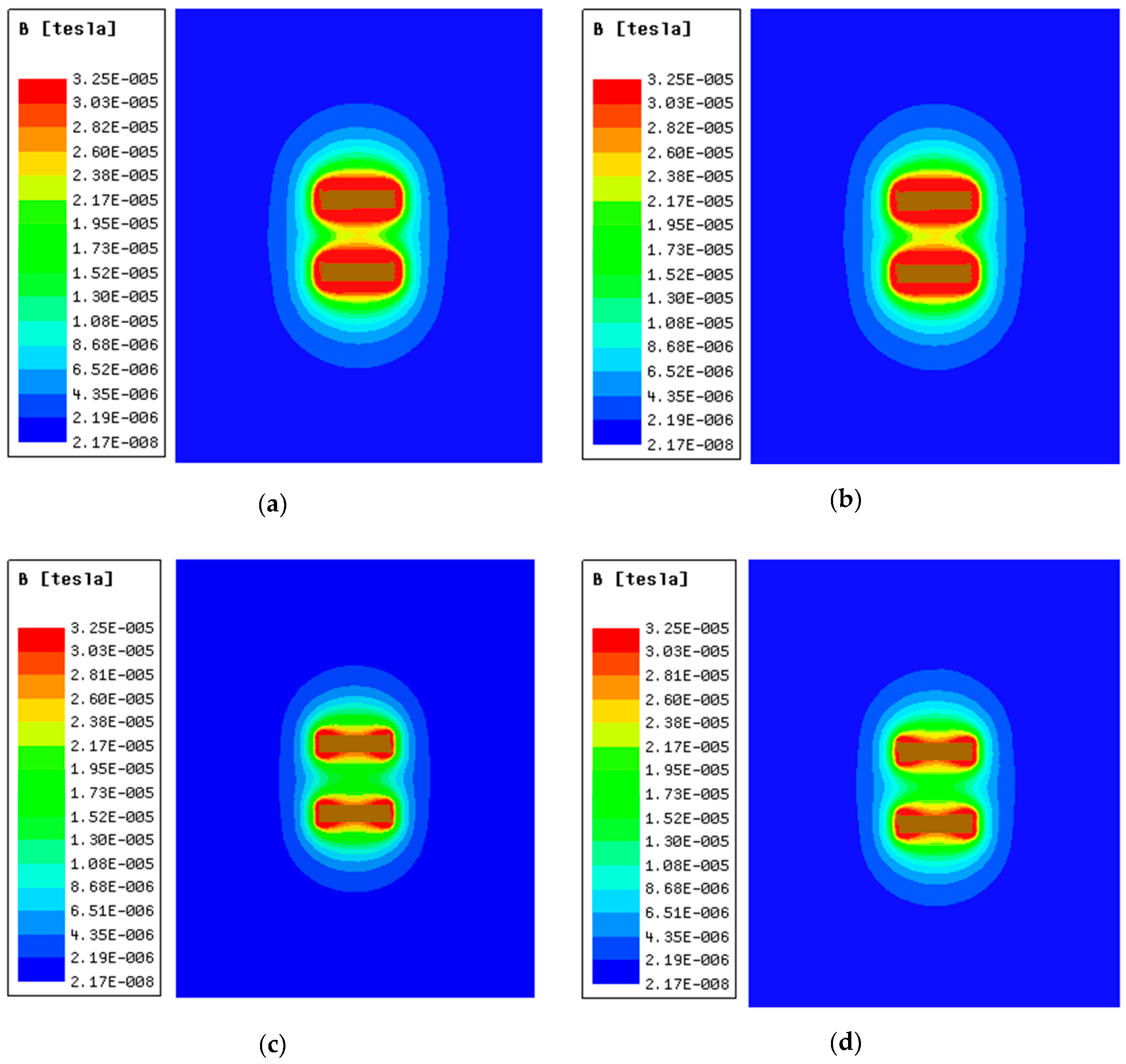
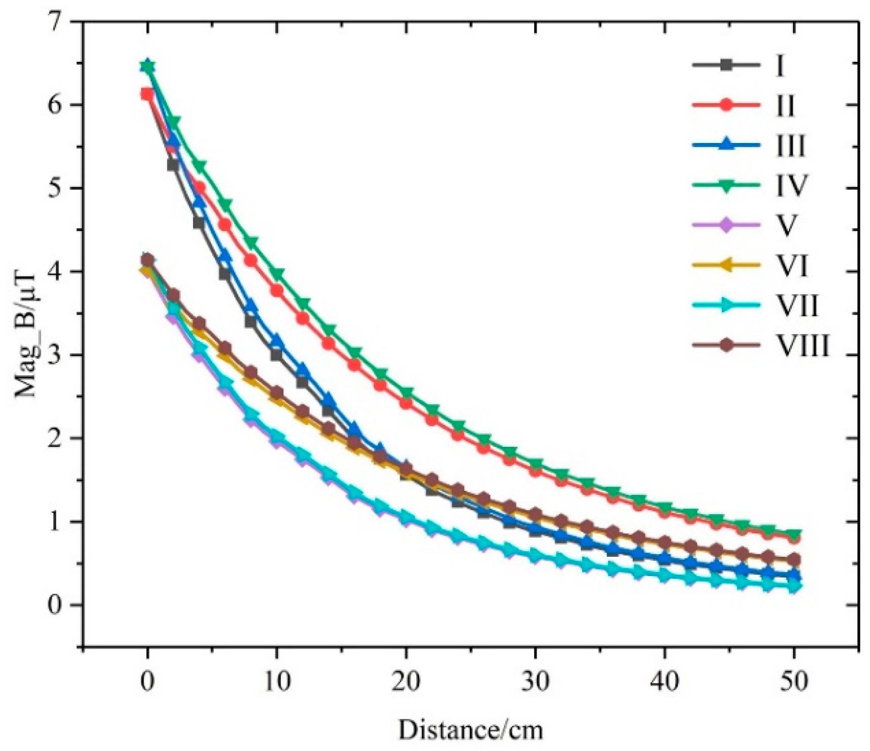
5. Simulation Result of B-Field Strength

A simulation model of wireless power transfer system was established according to the experimental platform as shown in Figure 9.
Four cases are considered in this paper: wireless power transfer system with RFC-type before optimization (Case 1); wireless power transfer system with RFC-type after optimization (Case 2); wireless power transfer system with PCL-type before optimization (Case 3); wireless power transfer system with PCL-type after optimization (Case 4). B-field strength results of the four cases are shown in Figure 10.
For further research on the B-field strength around the wireless power transfer system, we studied the B-field strength along the y-axis and the z-axis both from the specified point (0.0.3 m, 0.25 m) which was 0.1 m to the edge of the coils using the coordinate system in Figure 9.
The trends of the B-field strength along two lines in four cases are shown in Figure 11. ‘I’ represents B-field strength in case 1 along the y-axis; ‘II’ represents B-field strength in case 1 along the z-axis; ‘III’ represents B-field strength in case 2 along the y-axis; ‘IV’ represents B-field strength in case 2 along the z-axis; ‘V’ represents B-field strength in case 3 along the y-axis; ‘VI’ represents B-field strength in case 3 along the z-axis; ‘VII’ represents B-field strength in case 4 along the y-axis; ‘VIII’ represents B-field strength in case 4 along the z-axis. B-field strength around the system with the RFC-type is stronger than that with the PCL-type, while the B-field strength after optimization was stronger than that before optimization. In general, the B-field strength in the four cases was always less than 27 μT which is the reference level for general public exposure formulated by ICNIRP-2010.

6. Conclusions

In this paper, a steady-state matrix analysis method suitable for class-E power amplifier was introduced. Compared with the analysis process of the working principle of a class-E power amplifier, non-ideal factors are considered in this method, such as inductance resistance and leakage current, etc. The experimental results are more accurate. Based on steady-state matrix analysis, the output characteristic of two kinds of class-E power amplifier circuits were analyzed and optimized. The experimental results show that the output power of the two types of class-E power amplifier increased by 2.29 W (8.23%) and 1.91 W (7.35%), respectively, while the output efficiency had no obvious change. The B-field strength of the systems with two types of class-E power amplifier before and after optimization meets the ICNIRP-2010 standard.

Author Contributions

F.W. conceived and designed the study, and this work was performed under the advice of and regular feedback from him. R.L. was responsible for the simulations.

Funding

This work was supported by the Basic Research Program of Jiangsu Province (No. BK20180485), Jiangsu Provincial Key Laboratory of Smart Grid Technology and Equipment Project, and the Fundamental Research Funds for the Central Universities (No. 30919011241).

Conflicts of Interest

The authors declare no conflict of interest.

References

  1. Kkelis, G.; Yates, D.C.; Mitcheson, P.D. Class-E Half-Wave Zero dv/dt Rectifiers for Inductive Power Transfer. IEEE Trans. Power Electron. 2017, 32, 8322–8337. [Google Scholar] [CrossRef] [Green Version]
  2. Chokkalingam, B.; Padmanaban, S.; Leonowicz, Z. Class E Power Amplifier Design and Optimization for the Capacitive Coupled Wireless Power Transfer System in Biomedical Implants. Energies 2017, 10, 1409. [Google Scholar]
  3. Kwan, C.H.; Kkelis, G.; Aldhaher, S.; Lawson, J.; Yates, D.C.; Luk, P.C.K.; Mitcheson, P.D. Link efficiency-led design of mid-range inductive power transfer systems. In Proceedings of the 2015 IEEE PELS Workshop on Emerging Technologies: Wireless Power (2015 WoW), Daejeon Gwangyeoksi, Korea, 5–6 June 2015; pp. 1–7. [Google Scholar]
  4. Cai, W.; Zhang, Z.; Ren, X.; Liu, Y.-F. A 30-MHz isolated push-pull VHFresonantconverter. In Proceedings of the 2014 IEEE Applied Power Electronics Conference and Exposition-APEC, Fort Worth, TX, USA, 16–20 March 2014; pp. 1456–1460. [Google Scholar]
  5. Suetsugu, T.; Kazimierczuk, M. Analysis of transient behavior of class E amplifier due to load variations. In Proceedings of the 2011 IEEE Ninth International Conference on Power Electronics and Drive Systems, Singapore, 5–8 December 2011; pp. 600–603. [Google Scholar]
  6. Jaimes, A.F.; de Sousa, F.R. Simple expression for estimating the switch peak voltage on the class-E amplifier with finite DC-feed inductance. In Proceedings of the 2016 IEEE 7th Latin American Symposium on Circuits & Systems (LASCAS), Florianopolis, Brazil, 28 February–2 March 2016; pp. 183–186. [Google Scholar]
  7. Aldhaher, S.; Mitcheson, P.D.; Yates, D.C. Load-independent Class EF inverters for inductive wireless power transfer. In Proceedings of the 2016 IEEE Wireless Power Transfer Conference (WPTC), Aveiro, Portugal, 5–6 May 2016; pp. 1–4. [Google Scholar]
  8. Mury, T.; Fusco, V. Exploring figures of merit associated with the suboptimum operation of class-E power amplifiers. IET Circuits Devices Syst. 2007, 1, 401–407. [Google Scholar] [CrossRef]
  9. Raab, F. Idealized operation of the Class E tuned power amplifier. IEEE Trans. Circuits Syst. 1977, 24, 725–735. [Google Scholar] [CrossRef]
  10. Aldhaher, S.; Kkelis, G.; Yates, D.C.; Mitcheson, P.D. Class EF2 inverters for wireless power transfer applications. In Proceedings of the 2015 IEEE Wireless Power Transfer Conference (WPTC), Boulder, CO, USA, 13–15 May 2015; pp. 1–4. [Google Scholar]
  11. Choi, J.; Tsukiyama, D.; Tsuruda, Y.; Rivas, J. 13.56 MHz 1.3 kW resonant converter with GaN FET for wireless power transfer. In Proceedings of the 2015 IEEE Wireless Power Transfer Conference (WPTC), Boulder, CO, USA, 13–15 May 2015; pp. 1–4. [Google Scholar]
  12. Aldhaher, S.; Yates, D.C.; Mitcheson, P.D. Modelling and analysis of Class EF and Class E/F inverters with series-tuned resonant networks. IEEE Trans. Power Electron. 2016, 31, 3415–3430. [Google Scholar] [CrossRef]
  13. Mugisho, M.S.; Thian, M.; Grebennikov, A. Analysis and Design of a High-Efficiency Class-EM Power Amplifier. In Proceedings of the 2019 IEEE Radio and Wireless Symposium (RWS), Orlando, FL, USA, 20–23 January 2019; pp. 1–4. [Google Scholar]
  14. Beltran, R.A.; Raab, F.H. Simplified analysis and design of outphasing transmitters using class-E power amplifiers. In Proceedings of the 2015 IEEE Topical Conference on Power Amplifiers for Wireless and Radio Applications (PAWR), San Diego, CA, USA, 25–28 January 2015; pp. 1–3. [Google Scholar]
  15. Chadha, A.; Ayachit, A.; Saini, D.K.; Kazimierczuk, M.K. Steady-state analysis of PWM tapped-inductor buck DC-DC converter in CCM. In Proceedings of the 2018 IEEE Texas Power and Energy Conference (TPEC), College Station, TX, USA, 8–9 February 2018; pp. 1–6. [Google Scholar]
  16. Suetsugu, T.; Kazimierczuk, M. Comparison of class-e amplifier with nonlinear and linear shunt capacitance. IEEE Trans. Circuits Syst. I Fundam. Theory Appl. 2003, 50, 1089–1097. [Google Scholar] [CrossRef]
  17. Zhang, Z.; Lin, J.; Zhou, Y.; Ren, X. Analysis and Decoupling Design of a 30 MHz Resonant SEPIC Converter. IEEE Trans. Power Electron. 2016, 31, 4536–4548. [Google Scholar] [CrossRef]
  18. Guan, J.; Negra, R. Steady-state analysis and fast optimisation of Class-E power amplifiers with lossy switch for RF choke and finite DC-feed inductance. In Proceedings of the 2013 IEEE 56th International Midwest Symposium on Circuits and Systems (MWSCAS), Columbus, OH, USA, 4–7 August 2013; pp. 380–383. [Google Scholar]
  19. Reynaert, P.; Mertens, K.; Steyaert, M. A state-space behavioral model for CMOS class E power amplifiers. IEEE Trans. Comput. Aided Des. Integr. Circuits Syst. 2003, 22, 132–138. [Google Scholar] [CrossRef]
  20. Liang, J.; Liao, W. Steady-State Simulation and Optimization of Class-E Power Amplifiers With Extended Impedance Method. IEEE Trans. Circuits Syst. I Regul. Pap. 2011, 58, 1433–1445. [Google Scholar] [CrossRef]
  21. Zhou, J.; Morris, K.A.; Watkins, G.T.; Yamaguchi, K. Improved Reactance-Compensation Technique for the Design of Wideband Suboptimum Class-E Power Amplifiers. IEEE Trans. Microw. Theory Tech. 2015, 63, 2793–2801. [Google Scholar] [CrossRef] [Green Version]
  22. Khansalee, E.; Nuanyai, K.; Zhao, Y. Design and implementation of class E power amplifier with parallel circuit for wireless power transfer systems. In Proceedings of the 2017 International Electrical Engineering Congress (iEECON), Pattaya, Thailand, 8–10 March 2017; pp. 1–4. [Google Scholar]
Figure 1. Class-E model under ideal condition.
Energies 12 03240 g001
Figure 2. Class-E model under non-ideal condition.
Energies 12 03240 g002
Figure 3. (a) Output power of RFC changing with Lx and Cp; (b) output efficiency of RFC changing with Lx and Cp; (c) peak voltage of RFC changing with Lx and Cp.
Energies 12 03240 g003aEnergies 12 03240 g003b
Figure 4. (a) Output power of RFC changing with Lx and RL; (b) output efficiency of RFC changing with Lx and RL; (c) peak voltage of RFC changing with Lx and RL.
Energies 12 03240 g004
Figure 5. (a) Output power of PCL changing with Lin and Cp; (b) output efficiency of PCL changing with Lin and Cp; (c) peak voltage of PCL changing with Lin and Cp.
Energies 12 03240 g005
Figure 6. Experimental platform.
Energies 12 03240 g006
Figure 7. (a) Load current and voltage waveform of RFC before optimization; (b) load current and voltage waveform of RFC after optimization; (c) drain-source voltage waveform of PCL before optimization; (d) drain-source voltage waveform of PCL after optimization.
Energies 12 03240 g007
Figure 8. (a) Load current and voltage waveform of PCL before optimization; (b) load current and voltage waveform of PCL after optimization; (c) drain-source voltage waveform of PCL before optimization; (d) drain-source voltage waveform of PCL after optimization.
Energies 12 03240 g008
Figure 9. Simulation model of wireless power transfer system.
Energies 12 03240 g009
Figure 10. (a) Simulation result of B-field strength in case 1; (b) simulation result of B-field strength in case 2; (c) simulation result of B-field strength in case 3. (d) simulation result of B-field strength in case 4.
Energies 12 03240 g010
Figure 11. The trends of the B-field strength along two lines in four cases.
Energies 12 03240 g011
Table 1. Theoretical parameter values of class-E.
ParameterRFC TypePCL Type
RL_og(Ω)1228.4
L X _ o g ( μ H ) 0.3670
r L X ( Ω ) 0.190
C p _ o g ( n F ) 0.4050.639
L i n _ o g ( μ H ) 150.552
r L i n ( Ω ) 0.270.31
C 0 _ o g ( n F ) 0.3680.155
L 0 _ o g ( μ H ) 1.914.53
r L 0 ( Ω ) 0.450.87
Table 2. Parameter values of RFC before and after optimization.
ParameterIdeal ValueOptimized Value
L x ( μ H ) 0.3670.34
C p ( n F ) 0.4050.38
RL(Ω)129.12
P o ( W ) 28.1130.71
η ( % ) 90.3290.03
V ds max ( V ) 92.4195.01
Table 3. Parameter values of PCL before and after optimization.
ParameterIdeal ValueOptimized Value
L i n ( μ H ) 0.5520.54
C p ( n F ) 0.6390.6
P o ( W ) 26.5528.57
η ( % ) 90.3389.94
V ds max ( V ) 90.3596.90

