Article

Study of a Low-Power-Consumption Piezoelectric Energy Harvesting Circuit Based on Synchronized Switching Technology

1
Department of Instrumental and Electrical Engineering, Xiamen University, Xiamen 361005, China
2
Fujian Collaborative Innovation Center for R&D of Coach and Special Vehicle, Xiamen 361024, China
*
Author to whom correspondence should be addressed.
Energies 2019, 12(16), 3166; https://doi.org/10.3390/en12163166
Submission received: 20 June 2019 / Revised: 2 August 2019 / Accepted: 15 August 2019 / Published: 17 August 2019
(This article belongs to the Section L: Energy Sources)

Abstract

:
This paper presents a study of a piezoelectric energy harvesting circuit based on low-power-consumption synchronized switch technology. The proposed circuit includes a parallel synchronized switch harvesting on inductor interface circuit (P-SSHI) and a step-down DC-DC converter. The synchronized switch technology is applied to increase the conversion efficiency of the circuit. The DC-DC converter is used to accomplish the impedance matching for different loads. A low-power-consumption microcontroller and discrete components are used to build the P-SSHI interface circuit. The study starts with theoretical analysis and simulations of the P-SSHI interface circuit. Simulations and experiments were conducted to validate the theoretical analysis. The experimental results show that the maximum energy harvested by the system with a P-SSHI interface circuit is 231 μW, which is 2.89 times that of a system without the P-SSHI scheme. The power consumption of the P-SSHI interface circuit can be as low as 10.6 μW.

1. Introduction

In recent years, with the development of mobile devices and wireless sensor networks, the power supply issue of these mobile or wireless devices has attracted increased attention. Instead of chemical batteries, using the energy harvested from the ambient environment to power the electronic devices can avoid environmental pollution and battery replacement problems. Environmental energy sources including wind energy [1], solar energy [2], thermal energy [3] and kinetic energy [4] can be utilized. Among these energy sources, kinetic energy is ubiquitous and is becoming popular in energy harvesting [5].
A piezoelectric transducer is usually used to convert kinetic energy to electrical energy due to its high power density [5] and relatively high voltage [6]. As the output voltages of the piezoelectric elements in the harvesting system are alternating voltages, a rectifier interface circuit is usually needed. A commonly-used energy harvesting interface circuit is the bridge rectifier (BR) interface [7]. Its simple structure makes it easy to implement, and it has often been used to evaluate the power output of energy harvesting devices [8]. However, a drawback is its relatively low efficiency.
Synchronized switch technology was first proposed by Richard et al. [9] in their study into structural vibration damping using piezoelectric transducers. Subsequently, Richard et al. [10] proposed synchronized switch damping on inductor technology by adding an inductor in series with the switch. The switch was used to quickly inverse the piezoelectric voltage. Guyomar et al. [11] applied synchronized switch technology in a piezoelectric energy harvesting circuit and proposed synchronized switch harvesting on inductor (SSHI) technology. Following the research from Guyomar’s group, many researchers have studied energy harvesting circuits based on SSHI technology.
Krihely et al. [12] proposed a rectification scheme on the basis of SSHI, which was improved by adding a resonant circuit that commutates the voltage across the piezoelectric electrodes to eliminate the shunting of the current by the output capacitor. Experiments showed that the proposed scheme increased the extracted power by up to 230% compared to bridge rectifier interface under constant harmonic excitation. The problem with this solution is that the efficiency of the interface circuit is not much improved, as its control circuit consumes 35.2 μW of power. Liang et al. [13] proposed a P-S3BF interface circuit by optimizing the bias-flip strategy of the SSHI interface and verified that the power of the scheme was increased by 24.5% compared to the P-SSHI interface circuit. However, the overall power consumption of the control circuit was up to 6 mW. Wu et al. [14] proposed an optimal SSHI circuit integrated with an active rectifier; the proposed scheme inserted an active diode on each resonant loop, which ensured the flipping of the capacitor voltages at optimal times and eliminated the need to tune the switching time. The harvested power of the scheme was 2.1 times that of the bridge rectifier interface circuit, and the system dissipated about 24 μW.
The impedance matching problem is also important in piezoelectric energy harvesting systems. Kim et al. [15] showed in their research that when the impedance of the interface circuit matches the impedance of the piezoelectric transducer, the energy harvesting system collects the most power. In a weakly electromechanical coupled system, the equivalent impedance of the mechanical part is much larger than the circuit impedance, so more power can be harvested by increasing the circuit impedance. Liang et al. [16] presented the impedance model and analysis for piezoelectric energy harvesting systems with several interface circuits. The results showed that impedance-based analysis can predict the maximum harvested power well. To improve the efficiency of the energy harvesting circuit with different load impedances, a two-stage circuit topology was usually used. A two-stage energy extraction circuit was applied to provide good electrical load conditions for the piezoelectric energy harvester and supply a defined electrical voltage [17]. Kawai et al. [18] implemented a maximum power point tracking control in a piezoelectric energy harvesting circuit using switched inductors based on a two-stage circuit topology. In Chew and Zhu [19], a power extraction circuit and adaptive full analogue power management module allowed up to 156% more power to be harvested from the piezoelectric strain energy harvester. Zouari el al. [20] proposed an improved maximum power point tracking technique applied to the P-SSHI technique for piezoelectric vibration converters based on the fractional open circuit voltage method. The comparison between different simulation results showed that the proposed method improved the efficiency by about 279%.
From the above literature review, there are at least two important concerns in the study of piezoelectric energy harvesting interface circuits. Firstly, the power consumption of the interface circuit itself should be low; secondly, a two-stage circuit can be used to solve the impedance matching problem for different loads. In this paper, a low-power-consumption parallel synchronized switch harvesting on inductor interface circuit with an impedance matching circuit is proposed. The proposed system includes parallel synchronized switch harvesting on inductor interface circuit and a step-down DC-DC converter. An electromagnetic displacement sensor was used to detect the vibrating state of the piezoelectric beam. The feasibility of the system is verified by experiments. This paper is organized as follows. In Section 2, an overview of the proposed circuit system and theoretical analysis are given. In Section 3, the simulations of the P-SSHI and bridge rectifier interface are explored. In Section 4, the experiments and results are given. Finally, conclusions and discussions are presented in Section 5.

2. System Design and Theoretical Analysis
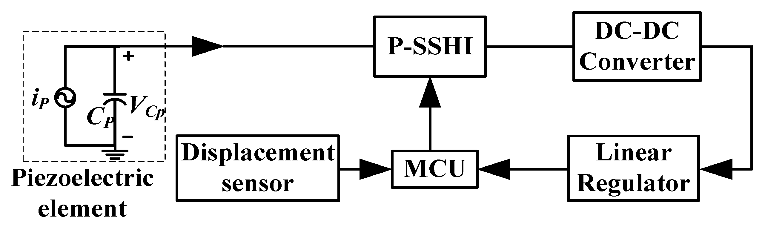
2.1. System Design

A piezoelectric element can be modeled as a sinusoidal current source ip in parallel with the piezoelectric capacitor Cp when the piezoelectric element vibrates in a sinusoidal manner [11,16], as shown in Equation (1).
i P ( t ) = I P sin ( ω t )
where IP and ω are the magnitude and frequency of the piezoelectric current source, respectively. The magnitude IP varies with the mechanical excitation level of the piezoelectric element.
The proposed piezoelectric energy harvesting system is shown in Figure 1. The interface circuit includes a P-SSHI and a DC-DC converter. The alternating voltage generated by the piezoelectric element is rectified to direct voltage through the P-SSHI interface circuit, the DC-DC converter provides an impedance matching function for the P-SSHI circuit, and the voltage output from P-SSHI is kept at a desired value. A linear regulator is used to regulate the output voltage of the DC-DC converter to a supplied voltage for the microcontroller (MCU). A displacement sensor is used to detect the motion state of the piezoelectric element.

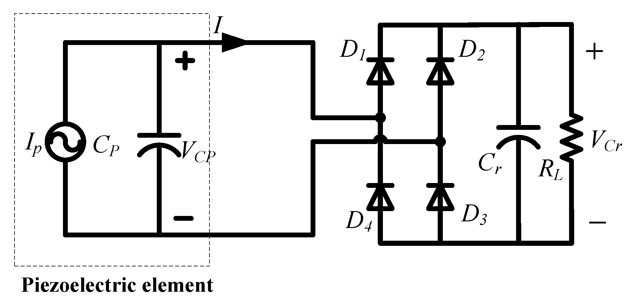
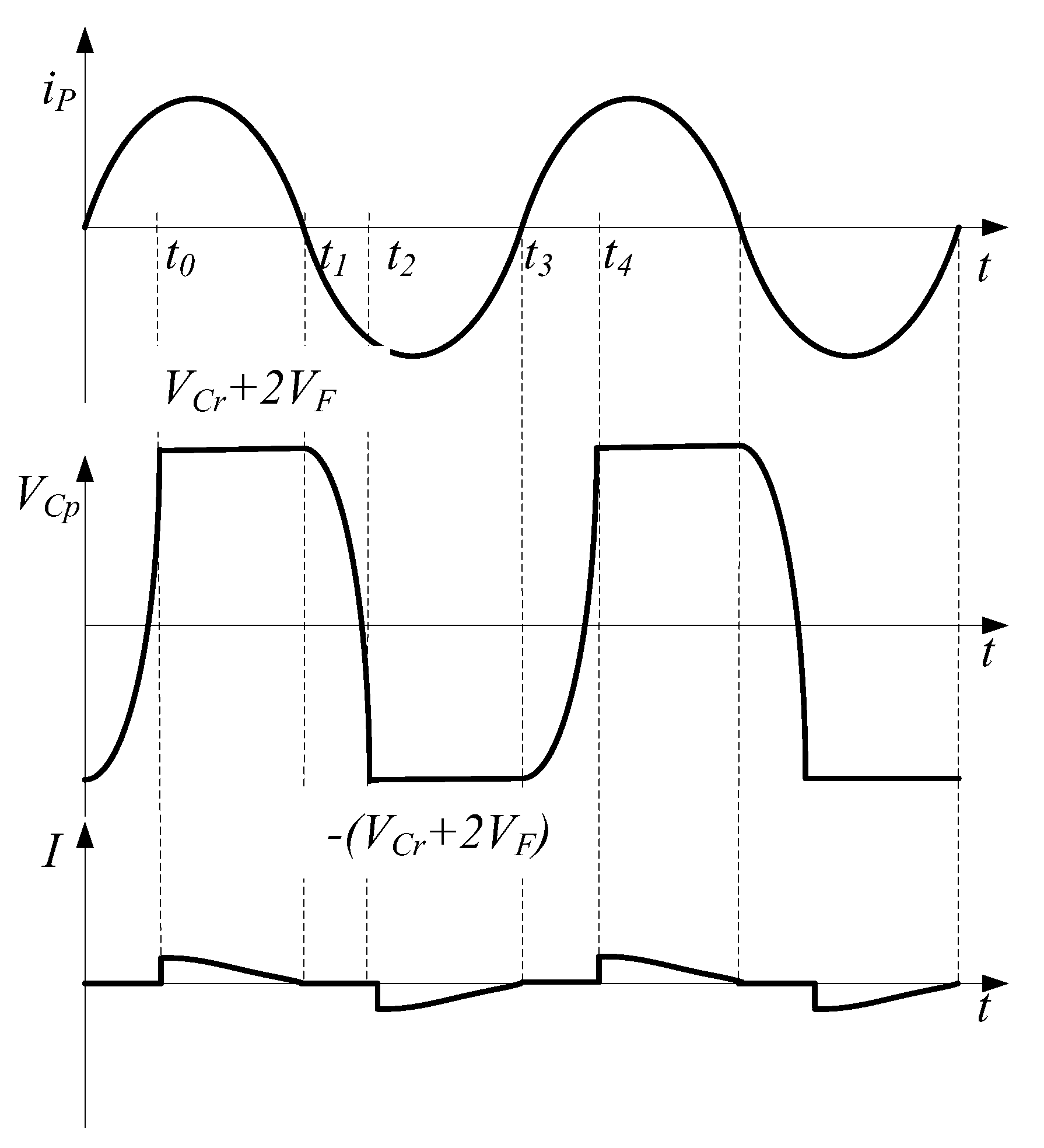
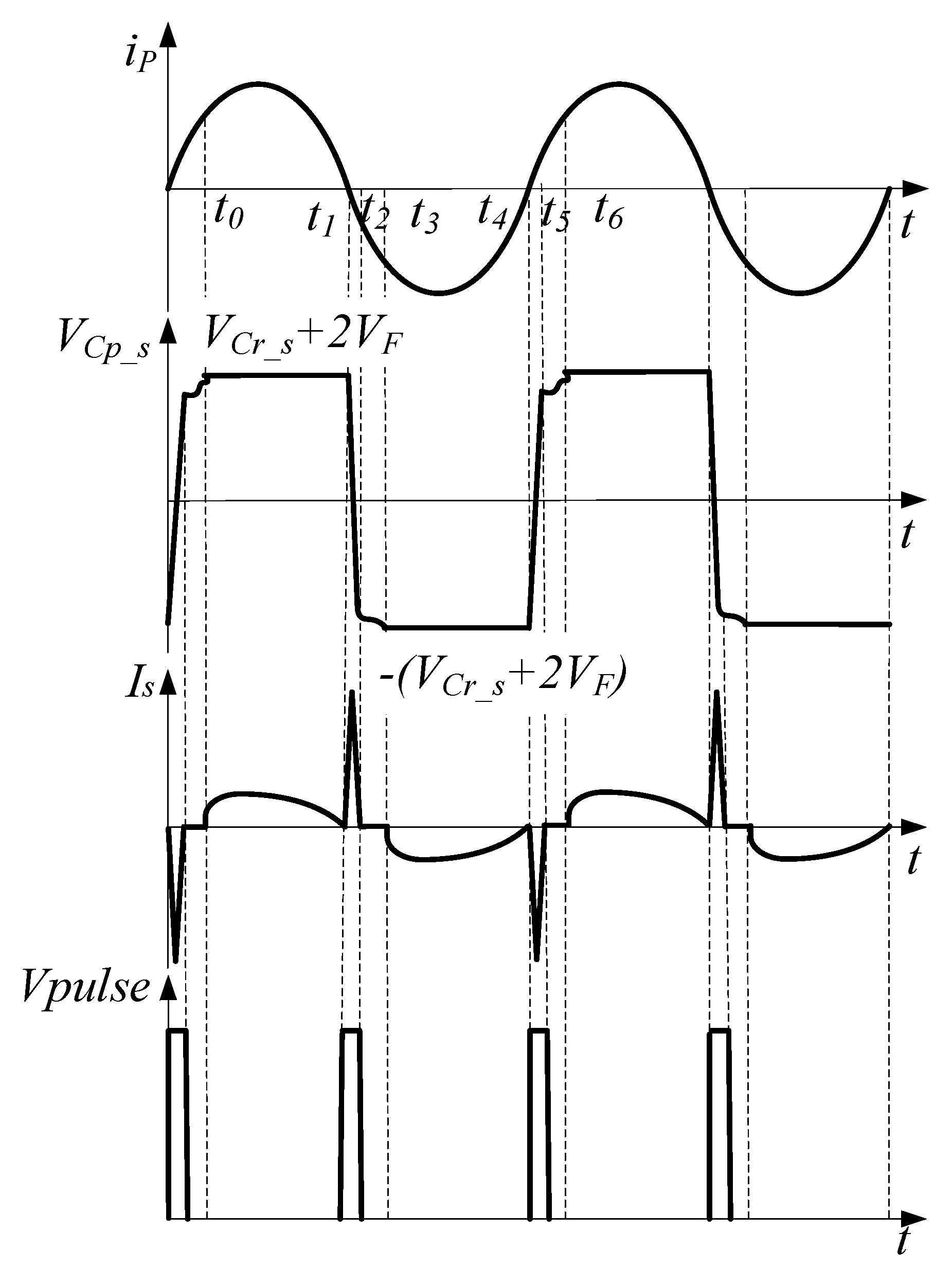
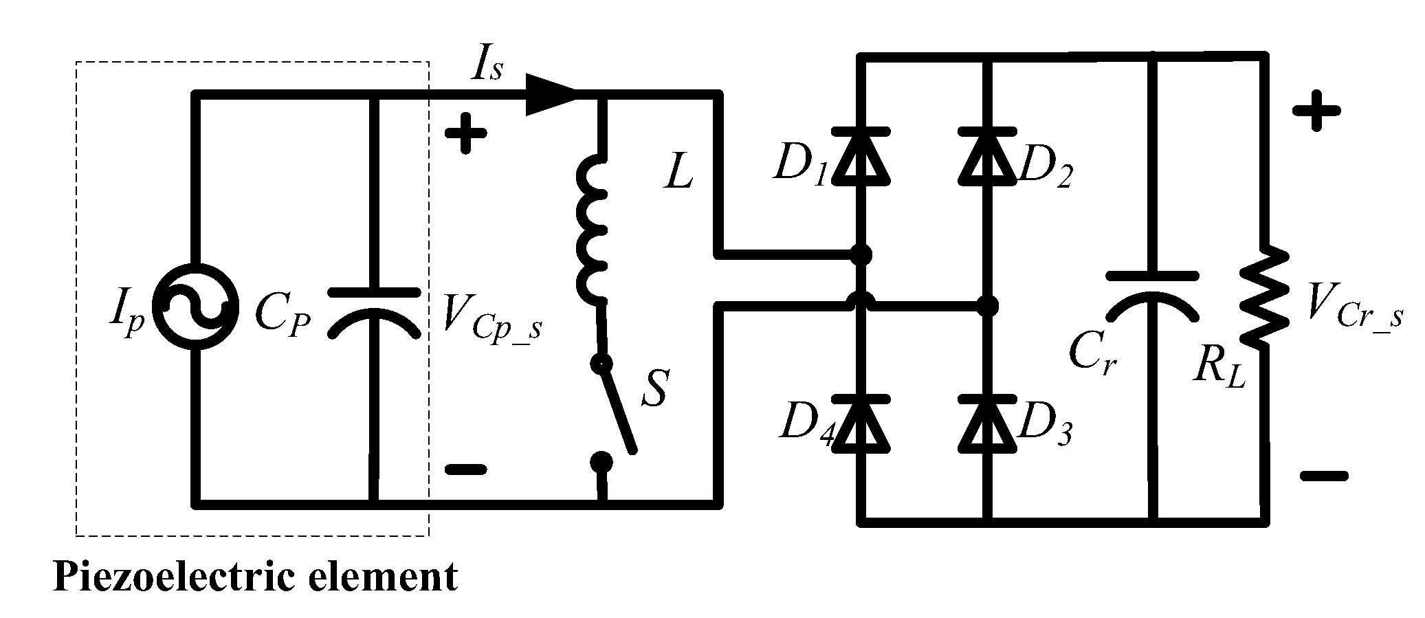
2.2. Interface Circuits and Theoretical Analysis

The modeling of the interface circuit and analysis of the output power and optimal impedance have been explored by many researchers [21,22,23], including the bridge rectifier and rectifier circuits based on switching technologies. A bridge rectifier interface circuit is shown in Figure 2. It consists of a full-bridge diode rectifier and a capacitor Cr. The working waveforms in the bridge rectifier interface circuit are shown in Figure 3.
In half a cycle, the total amount of charge flowing out of the piezoelectric generator is expressed as follows:
0 T / 2 I d t = 0 T / 2 ( α μ C P V ) d t = 2 ( α U M C P V C r )
where α is the force factor, I and V are the outgoing current and voltage, μ and UM are the displacement of the mechanical vibration and the amplitude of the mechanical vibration displacement, and T is the period.
The total amount of charge flowing through the load is as follows:
0 T / 2 i r d t = T V C r 2 R L
where ir is the current flowing through the load.
From Equations (2) and (3),
V C r = 2 α U M R L ω 2 C P R L ω + π
Thus, the harvested power can be calculated as
P = V C r 2 R L = 4 α 2 U M ω 2 R L ( 2 R L C P ω + π ) 2
When the piezoelectric generator vibrates at a certain amplitude, according to Equation (5), there exists an optimal value Ropt to obtain the maximum harvested power. Let dP/dRL = 0, and the optimal load is as follows:
R o p t = π 2 C P ω
The maximum power is
P M A X = ω α 2 U M 2 2 π C P
The P-SSHI interface circuit is shown in Figure 4. It consists of a piezoelectric element, an inductor L, a switch S, a full-bridge diode rectifier, and a capacitor Cr. Compared with the bridge rectifier, the P-SSHI introduces an inductor L and a switch S connected in parallel with the piezoelectric capacitor CP. The inductor L and the piezoelectric capacitor CP form a resonant circuit to invert the voltage across the piezoelectric capacitor VCp_s when needed.
The working waveforms of the P-SSHI are shown in Figure 5. In the time interval t0t1, the current source iP is in the positive half cycle, diodes D1 and D3 are turned on, the switch S turns off, and the current source iP charges the capacitor Cr. During this time period, the voltage across the piezoelectric capacitor VCp_s is greater than the sum of the forward voltages of the diodes and the voltage across the capacitor VCr_s. In the time interval t1t2, the current source iP starts to reverse, the voltage VCp_s drops, and the full-bridge diode rectifier is disconnected. The switch S is turned on, and the voltage VCp_s is quickly turned in reverse. After a certain time (a half-cycle of the LC resonant circuit), the switch S is turned off, and the circuit enters the interval t2t3. In the time interval t2t3, the current source iP continues to charge the piezoelectric capacitor CP. When the voltage across the piezoelectric capacitor VCp reaches the value of −(Vcr_s + 2VF), where VF is the forward voltage drop of the diodes, diodes D2 and D4 are turned on, the piezoelectric capacitor CP charges the capacitor Cr, and it enters the interval t3–t4. In the interval t3–t6, the working procedure is similar to the interval t0–t3. Compared to the bridge rectifier, less charge is used to neutralize the remaining charge, so more charge flows to the load.
In the above process, the switch S is turned on when the current IP reaches zero. At that moment, the cantilever beam vibration amplitude reaches the maximum positive or negative values. The piezoelectric capacitor CP and the inductor L form an LC resonant tank, and the voltage VCp changes in a short interval τ = π L C P . After that, the voltage VCp_s is flipped from VCr_s to Vm, where Vm is the flipped voltage. The flipping factor γ is related to the quality factor Q of the LC resonant circuit by
V m = γ V C r _ s = e π 2 Q V C r _ s ( 0 < γ < 1 )
In half a cycle, the total amount of charge flowing out of the piezoelectric generator is expressed as
0 T / 2 I s d t = 0 T / 2 ( α μ C P V ) d t = 2 ( α U M C P V C r _ s )
The amount of charge flowing out of the piezoelectric generator is composed of the charge flowing through the inductor L and the load.
0 T / 2 i L d t = C P ( V C r _ s V m )
0 T / 2 i r _ s d t = T V C r _ s 2 R L
where iL is the current flowing through the inductance, and ir_s is the current flowing through the load.
From Equations (8)–(11),
V C r _ s = 2 α U M R L ω ( 1 γ ) C P R L ω + π
Therefore, the power harvested by the P-SSHI interface circuit is
P s = V C r _ s 2 R L = 4 α 2 ω 2 U M 2 R L [ R L C P ω ( 1 γ ) + π ] 2
Let dPs/dRL = 0; the harvested power reaches a maximum PMAX_s for an optimal load Ropt_s:
R o p t _ s = π 2 C P ω
The maximum harvest power is
P M A X _ s = ω α 2 U M 2 π C P ( 1 γ )

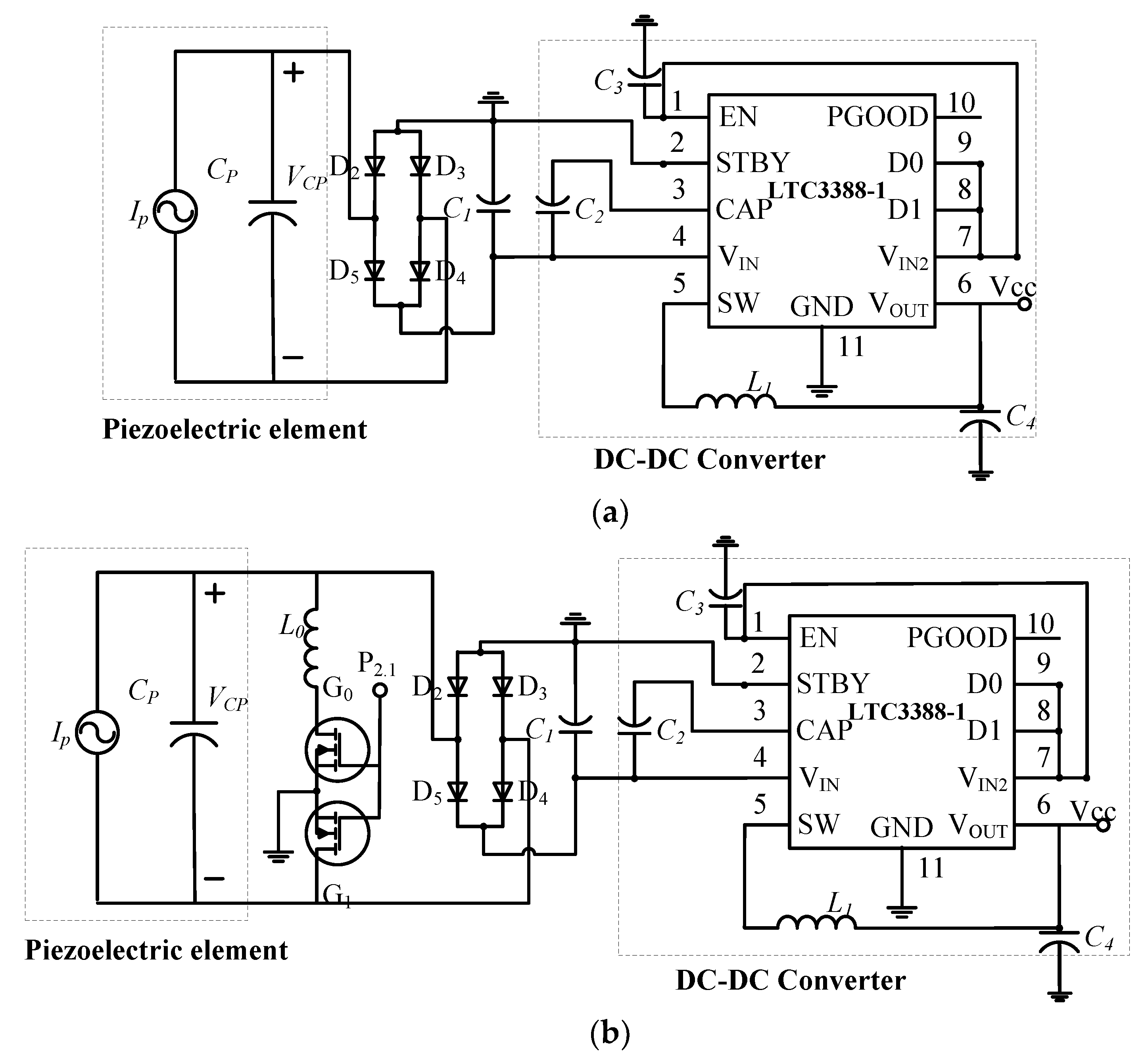
2.3. DC-DC Converter
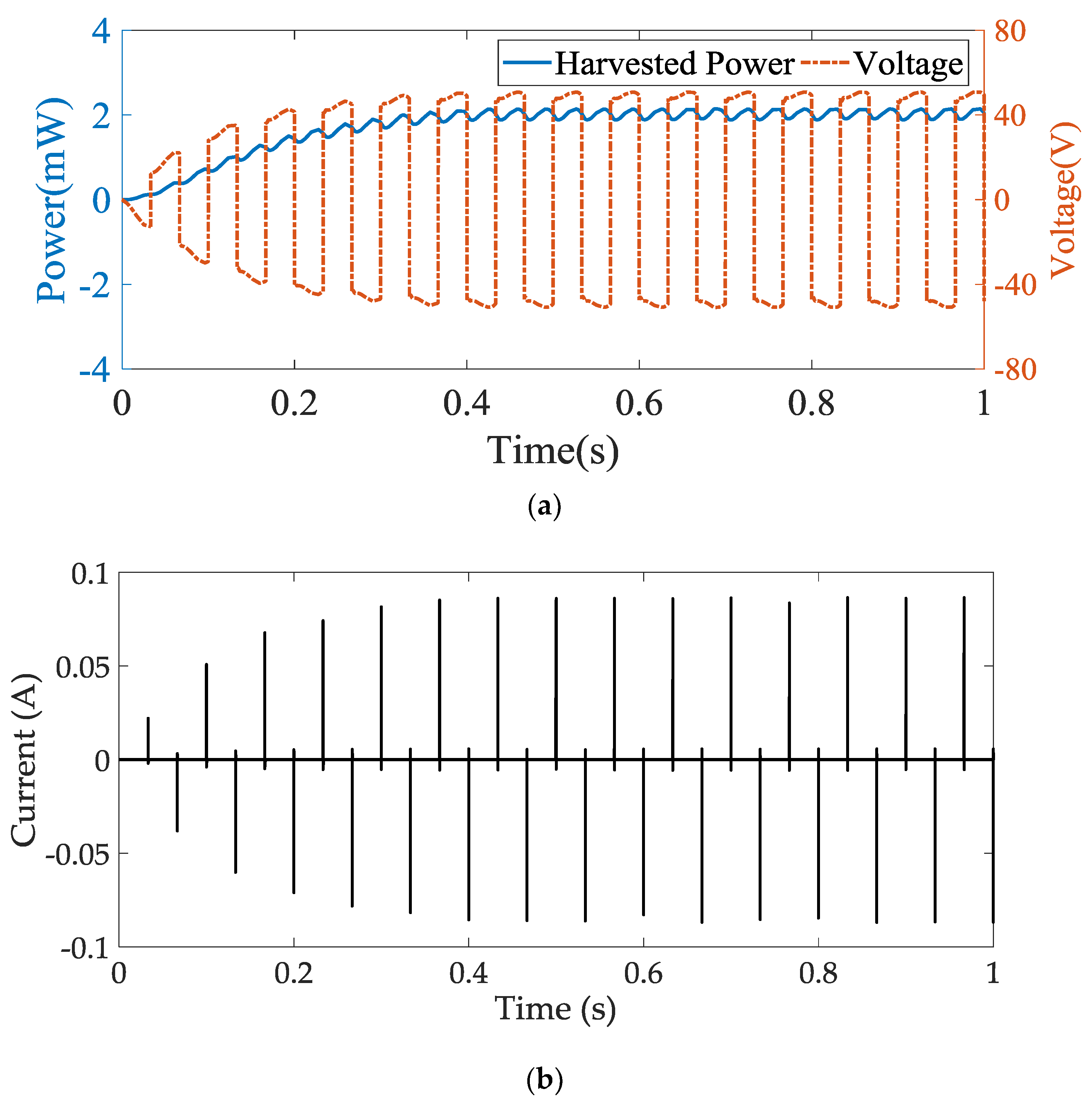
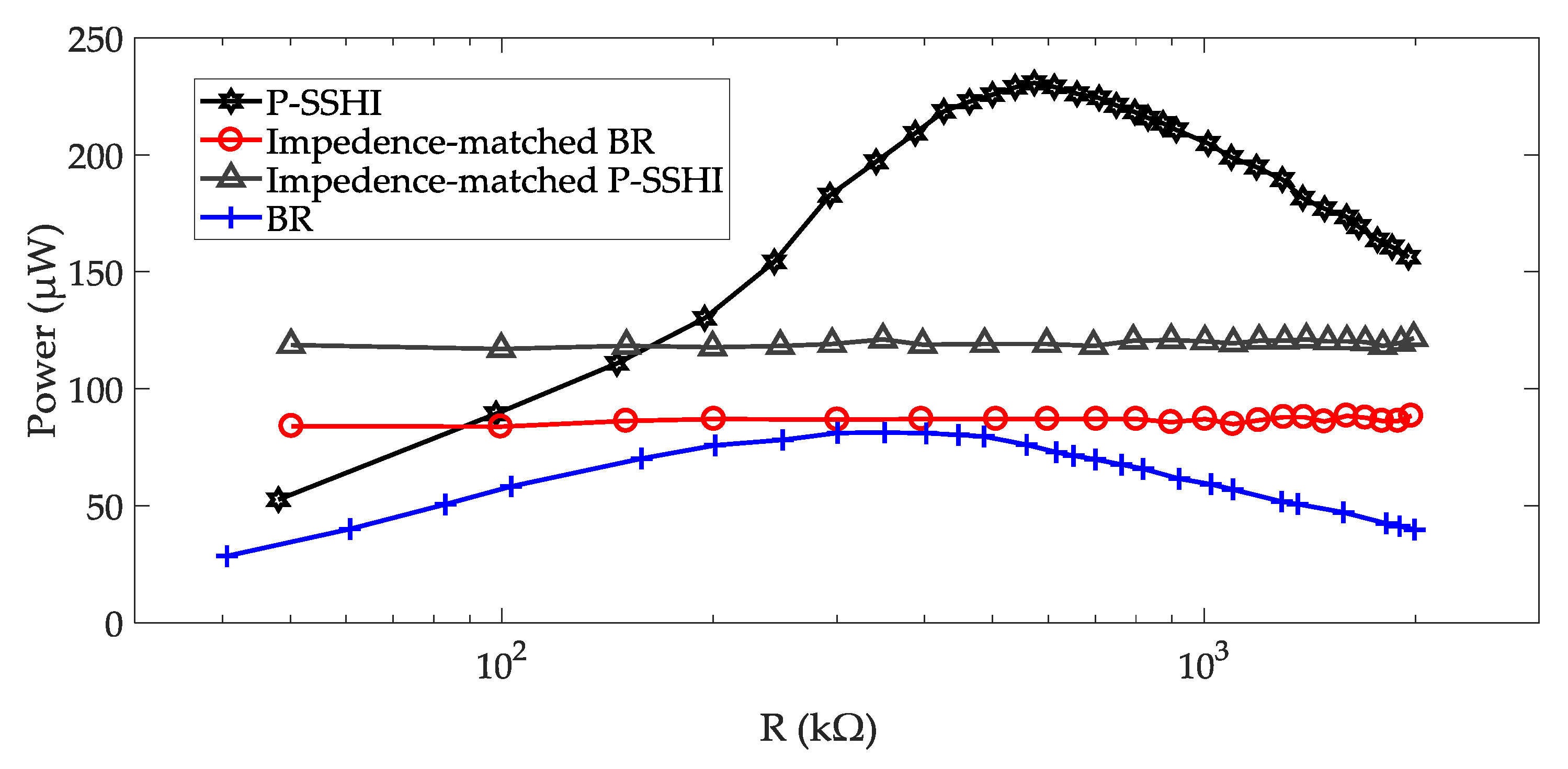
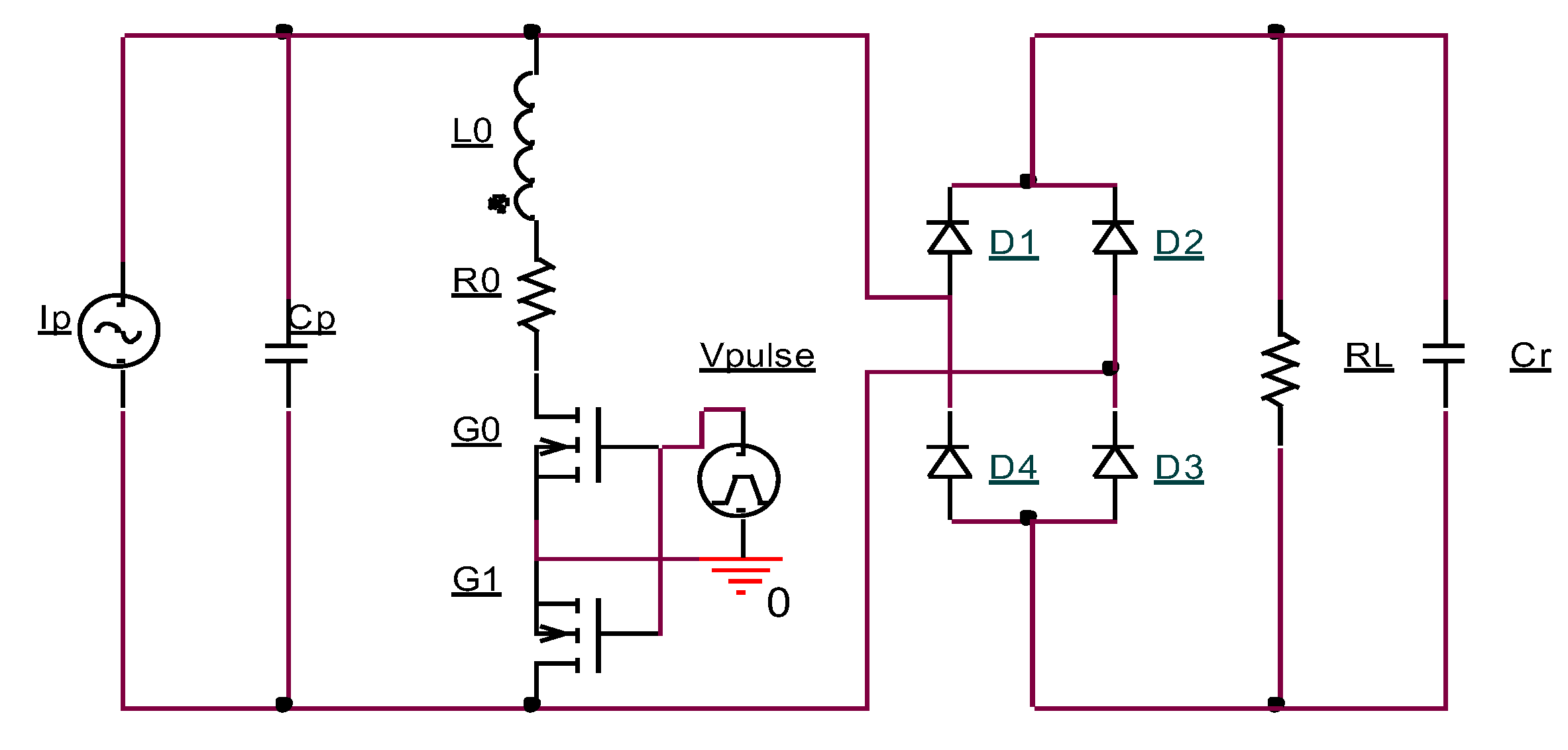
Previous analysis shows that the output power of the bridge rectifier interface and the P-SSHI interface are affected by the value of the load. Therefore, a DC-DC converter is connected to the interface circuit to form an optimal load for the interface circuit. Piezoelectric generators can generate peak voltages of a few volts to tens of volts—much larger than the voltage usually required by an electronic device; for example, a wireless sensor network node—therefore, a step-down DC-DC converter was applied to lower the output voltage. In this research, a commercial DC-DC converter, LTC3388-1 step-down regulator from Analog Devices, with a wide working voltage range of 2.7 V to 20 V and optional output voltages of 1.2 V, 1.5 V, 1.8 V, and 2.5 V was used. The LTC3388-1 is connected to the bridge rectifier interface circuit and the P-SSHI interface circuit to construct an impedance-matched bridge rectifier circuit and an impedance-matched P-SSHI circuit, as shown in Figure 6a,b, respectively.
In the impedance-matched P-SSHI interface circuit, as shown in Figure 6b, the switch connected in series with the inductor L as shown in Figure 4 is built by two N-channel Metal-Oxide-Semiconductor Field-Effect Transistors (MOSFETs) connected in series. The source electrodes of the two MOSFETs are connected together to the ground to build an appropriate potential for the interface circuit. The grid electrodes of the two MOSFETs are controlled by the I/O port P2.1 of the microcontroller. When port P2.1 outputs a high-level voltage, both MOSFETs turn on.

3. Simulations

The proposed circuits were built in the Personal Computer Simulation Program with Integrated Circuit Emphasis (PSPICE) simulation software to verify the theoretical analysis. The P-SSHI interface circuit in the simulation is shown in Figure 7. The frequency of the current source iP was set to 15 Hz and the current amplitude was 80 μA. The internal capacitance CP was 15 nF, the inductance L was 4.7 mH, and the resistance of the inductor L was set to 4 Ω. G0 and G1 are MOSFETs (modeled BSS138/FAI). The rectifier bridge diodes D1D4 were modeled D1N4004, and the forward voltage was 0.53 V. The capacitance of Cr was 0.1 μF. Vpulse is a pulse–width modulation (PWM) control signal, whose low level, high level, rise time and fall time of the control voltage were set to 0 V, 10 V, 0.01 μs, 0.01 μs, respectively. Vpulse was connected to switches G0 and G1. When the current source ip started to reverse, Vpulse turned to high and was applied to G0 and G1 to turn on the switches.
The first simulation was performed to verify the working waveforms of the P-SSHI interface circuit in the analysis. The resultant waveforms in the simulation are shown in Figure 8. Figure 8a shows the harvested power of the load and the voltage across the piezoelectric capacitor. It can be seen from the figure that the voltage across the piezoelectric capacitor quickly flipped, and the flipping factor was around 0.95. Figure 8b shows the current flowing from the piezoelectric element to the load. There are currents peaks during every voltage flip. The waveforms in the simulation are consistent with the theoretical analysis.
The second simulation was performed to verify the analysis shown in Equation (14). The simulated system resulted in different harvested power by changing the load resistance, as shown in Figure 9. The simulation results show that when the load RL was 1170 kΩ, the harvested power reached the maximum of 2136 μW. The theoretical optimal load calculated by Equation (14) is 1111 kΩ, which is slightly lower than that in the simulation. The reason for this may be that the parasitic elements (capacitance, resistance, inductance) of the bridge rectifier were not taken into account in the theoretical analysis.
The third simulation was carried out to compare the harvested power between the P-SSHI circuit and the bridge rectifier circuit. A bridge rectifier circuit was also built in the software but is not shown in the paper. By changing the load, the harvested power of the bridge rectifier circuit is shown as the circle-marked curve in Figure 9. For the bridge rectifier interface circuit, the maximum harvested power is 709 μW. The P-SSHI interface circuit outputs 301% more power than the bridge rectifier interface circuit.

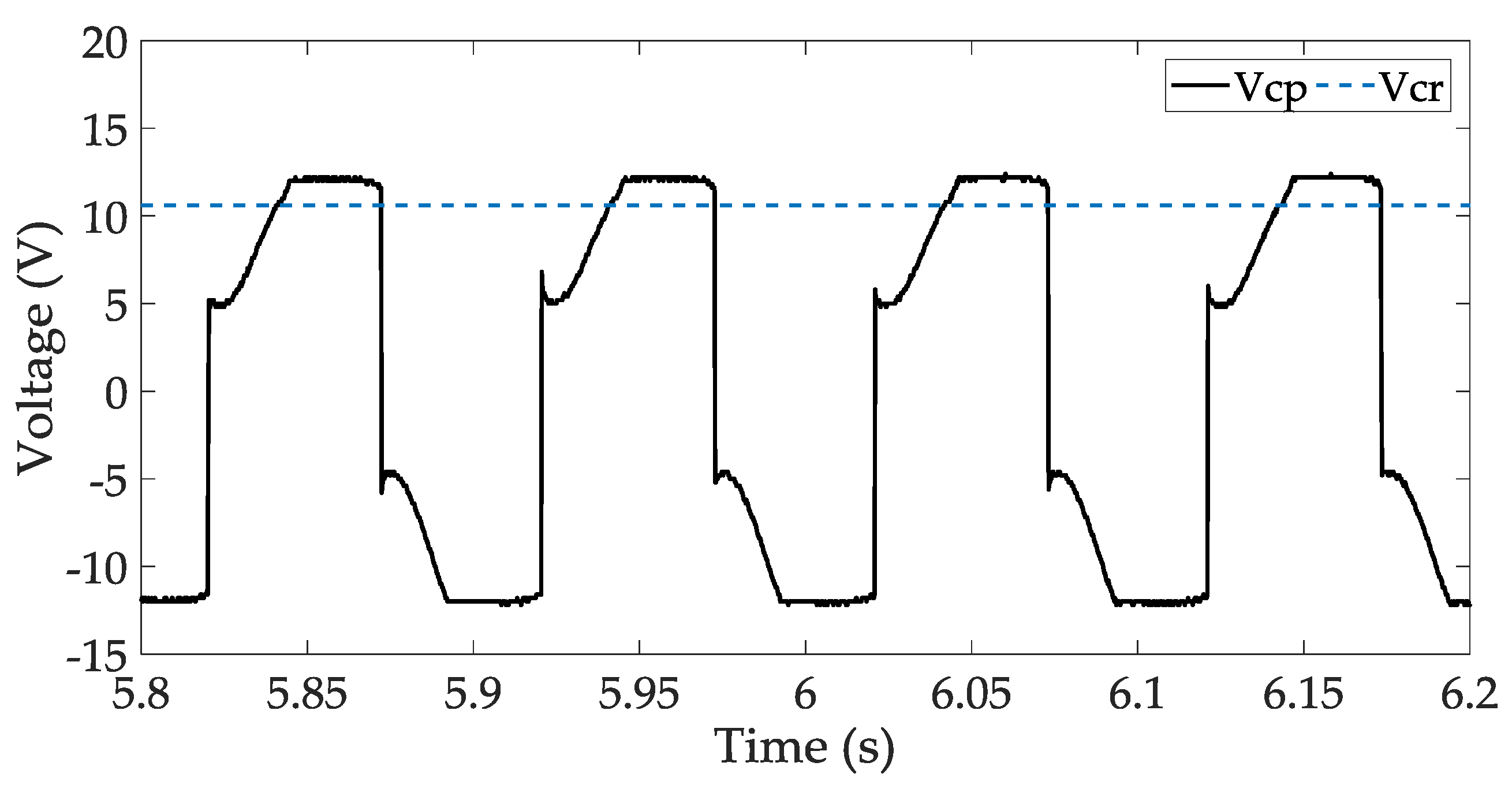
4. Experimental Validations

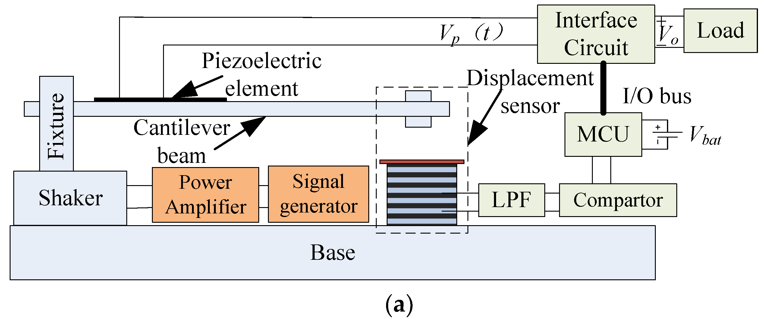
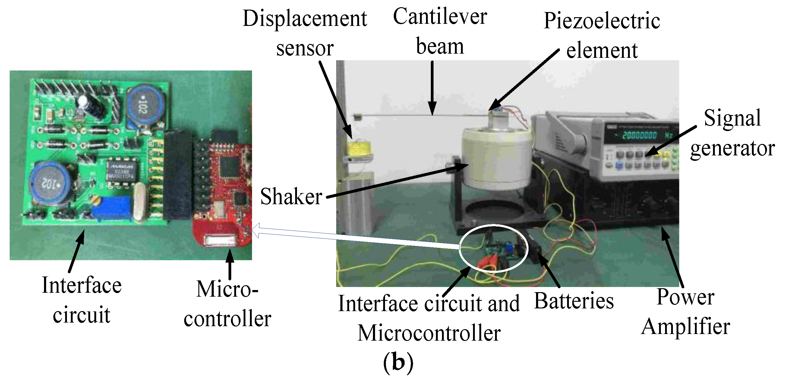
4.1. Prototype and Experimental Setup

The block diagram of the experimental setup is shown in Figure 10a. The real experimental setup is shown in Figure 10b. The piezoelectric energy harvesting system is composed of a piezoelectric cantilever beam and the interface circuit. The cantilever beam is made of aluminum. The piezoelectric element is modeled as QP21B (Mide, Woburn, MA, USA). The QP21B is a bimorph piezoelectric device that is packaged in protective polymide layers, which significantly increases the robustness of the piezoelectric elements. The piezoelectric element was surface-mounted on the cantilever beam, 2 mm away from the clamped end. The sizes of the cantilever beam and the piezoelectric element are shown in Table 1. The cantilever beam was mounted on a shaker (JZK-5, Sinocera piezotronics, Yangzhou, China). The shaker is connected to a power amplifier (YE5871A, Sinocera piezotronics, Yangzhou, China) and a signal generator ATF20A (ATTEN, Shenzhen, China).
To detect the displacement of the cantilever beam, a magnet is fixed on the free end of the cantilever beam, offering a varying magnetic field while the beam vibrates. A coil is used as the displacement sensor. The output voltage of the coil is connected to a low-pass filter (LPF) circuit and a zero-crossing comparator to determine the extreme displacement points of the cantilever beam. The resultant signal is sent to the microcontroller through the I/O port P1.6. The MSP430 (Texas Instruments, Dallas, TX, USA) is applied as the microcontroller to control the switches in the circuits and process the received signals. Other parameters of the experimental system are shown in Table 1.

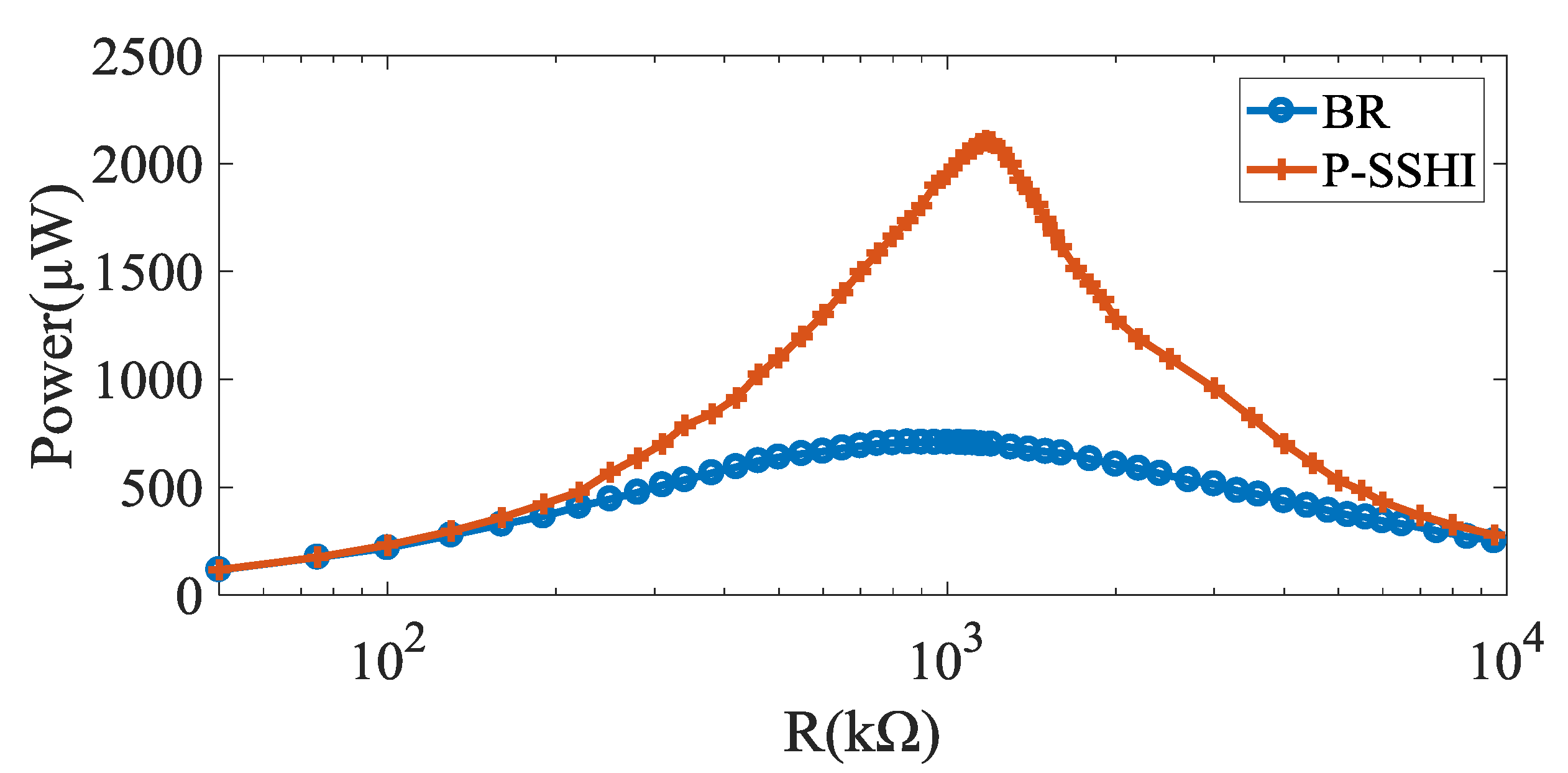
4.2. Experimental Results

Under an excitation level with the amplitude of the open-circuit voltage of the piezoelectric element of 12.2 V, the experimental voltage waveforms of P-SSHI are shown in Figure 11. The voltage waveform is similar to the theoretical analysis and simulation waveform. However, the voltage flipping factor is only 0.41. The flipping factor is much lower than the flipping factor in the simulation. The reason for this may be that the components in the simulation are built in an ideal model, and in the real case, the power consumptions of the components are much larger. The power consumption of the whole system mainly includes the power consumption from the microcontroller, the zero-crossing comparator and the switches. The MSP430 microcontroller (Texas Instruments, Dallas, TX, America) is set to operate in low-power mode 1 and low-power mode 4. In low-power mode 1, the MCU with a 1 MHz crystal frequency consumes 600 μW. In low-power mode 4, the MCU consumes 1.5 μW. To lower the power consumption of the microcontroller, the MCU works mainly under low-power mode 4, waiting for the interrupt signal from the zero-crossing comparator. When the interrupt signal is triggered, the MCU will generate a high-level voltage to control the switches G0 and G1, and then it will enter low-power mode 4 again. By doing so, the average power consumption will be very low. From the experiments, the average power consumption of the MCU is only 1.72 μW. The average power consumption of the SSHI interface circuit is only 10.6 μW.
Figure 12 shows the harvested power of the four interface circuits with different load resistances. The harvested power of the bridge rectifier (BR) interface circuit is shown in the plus-marked curve. When the load resistance RL is 447 kΩ, a maximum power of 80.26 μW was harvested. The harvested power of the P-SSHI interface circuit is shown in the star-marked curve. The maximum power is 230.74 μW while the load is 573 kΩ. The maximum harvested power of the P-SSHI interface circuit is 2.87 times that of the bridge rectifier interface circuit.
The output power of the impedance-matched circuits was also tested. A fixed 2.5 V output voltage was offered to power the load. From the triangle-marked curve and the circle-marked curve shown in Figure 12, it is found that, although the load resistance changed, the output power in these two cases both remained at a stable level. For the impedance-matched bridge rectifier circuit, the output power of the bridge rectifier circuit is maintained around 82 μW. For the impedance-matched P-SSHI circuit, the output power of the interface circuit is maintained around 120 μW. The harvested power of the impedance-matched P-SSHI interface circuit is 1.47 times that of the impedance-matched bridge rectifier interface circuit. However, the output power of the impedance-matched P-SSHI interface circuit is lower than the maximum output power of the P-SSHI interface circuit. The reasons for this may be that too much power is consumed by the DC-DC converter, and the input voltage of the commercial DC-DC converter is not optimal for the P-SSHI interface circuit. In order to increase the harvested power of the impedance-matched P-SSHI interface circuit, the DC-DC converter should be tailor-made with the P-SSHI interface circuit.

5. Conclusions and Discussion

A low-power-consumption interface circuit with an impedance-matched scheme for a piezoelectric energy harvesting system is presented in this paper. The interface circuit integrates the P-SSHI circuit and a step-down DC-DC converter to modify the impedance of the load. For comparison, a P-SSHI circuit, a bridge rectifier circuit and an impedance-matched bridge rectifier circuit were also built. Under a constant excitation level, the designed interface circuits are applied to harvest the power with varying load. The experimental results showed that, compared to the bridge rectifier interface circuit, the output power of the P-SSHI interface circuit increased by 287%. For the impedance-matched P-SSHI interface circuit, the harvested power is 1.47 times that of the impedance-matched bridge rectifier interface circuit. It is shown that the harvested power with P-SSHI technology is significantly improved compared to the bridge rectifier interface circuit. Low-power-consumption schemes are applied to control the P-SSHI interface circuit. The experimental results showed that the average power consumption of the microcontroller is only 1.72 μW, and the average power consumption of the SSHI interface circuit is only 10.6 μW. The impedance-matched P-SSHI interface can maintain a stable output power for different load resistances. However, the output power of the impedance-matched P-SSHI interface circuit is lower than the maximum output power of the P-SSHI interface circuit. The reason for this may be that the commercial DC-DC converter used in the circuit cannot offer an optimal voltage for the P-SSHI circuit, and the DC-DC converter itself consumed too much power.
Future work will include the design of a tailor-made DC-DC converter and low-power-consumption displacement sensing system. Also, an integrated system based on monolithic integrated circuit will help to improve the system efficiency.

Author Contributions

Conceptualization, J.H. and M.G.; methodology, J.H. and M.G.; software, J.H., F.C. and M.H.; validation, J.H., F.C., M.H. and S.W.; formal analysis, W.C., J.H. and M.G.; investigation, J.H., F.C. and M.H.; resources, W.C. and M.G.; data curation, J.H., F.C. and M.G.; writing—original draft preparation, J.H. and M.G.; writing—review and editing, M.G.; visualization, M.G.; supervision, M.G.; project administration, M.G.; funding acquisition, W.C. and M.G.

Funding

This research was funded by National Natural Science Foundation of China (NSFC), grant number 51777177; NSFC grant number 51707168; and Key Projects of Fujian Collaborative Innovation Center for R&D of Coach and Special Vehicle, grant number 2016AYF002.

Conflicts of Interest

The authors declare no conflict of interest.

References

  1. An, X.Y.; Song, B.W.; Tian, W.L.; Ma, C.C. Design and CFD simulations of a vortex-induced piezoelectric energy converter (VIPEC) for underwater environment. Energies 2018, 11, 330. [Google Scholar] [CrossRef]
  2. Vasiliev, M.; Nur-E-Alam, M.; Alameh, K. Recent developments in solar energy-harvesting technologies for building integration and distributed energy generation. Energies 2019, 12, 1080. [Google Scholar] [CrossRef]
  3. Ando Junior, O.H.; Calderon, N.H.; de Souza, S.S. Characterization of a thermoelectric generator (TEG) system for waste heat recovery. Energies 2018, 11, 1555. [Google Scholar] [CrossRef]
  4. Choi, Y.M.; Lee, M.G.; Jeon, Y. Wearable biomechanical energy harvesting technologies. Energies 2017, 10, 1483. [Google Scholar] [CrossRef]
  5. Roundy, S.; Leland, E.S.; Baker, J.; Carleton, E.; Reilly, E.; Lai, E.; Otis, B.; Rabaey, J.M.; Wright, P.K.; Sundararajan, V. Improving power output for vibration-based energy scavengers. IEEE Pervasive Comput. 2005, 4, 28–36. [Google Scholar] [CrossRef]
  6. Elahi, H.; Eugeni, M.; Gaudenzi, P. A review on mechanisms for piezoelectric-based energy harvesters. Energies 2018, 11, 1850. [Google Scholar] [CrossRef]
  7. Liu, W.Q.; Feng, Z.H.; He, J.; Liu, R.B. Maximum mechanical energy harvesting strategy for a piezoelement. Smart Mater. Struct. 2007, 16, 2130–2136. [Google Scholar] [CrossRef]
  8. Shu, Y.C.; Lien, I.C. A comparison between the standard and SSHI interfaces used in piezoelectric power harvesting. In Proceedings of SPIE, Active & Passive Smart Structures and Integrated Systems; Society of Photo Optical: Bellingham, WA, USA, 2007; Volume 6525, p. 652509. [Google Scholar] [CrossRef]
  9. Richard, C.; Guyomar, D.; Audigier, D.; Ching, G. Semi-passive damping using continuous switching of a piezoelectric device. In Proceedings of SPIE, Smart Structures and Materials 1999: Passive Damping and Isolation; International Society for Optics and Photonics: Bellingham, WA, USA, 1999; Volume 3672, pp. 104–111. [Google Scholar] [CrossRef]
  10. Richard, C.; Guyomar, D.; Audigier, D.; Bassaler, H. Enhanced semi-passive damping using continuous switching of a piezoelectric device on an inductor. In Proceedings of SPIE, Smart Structures and Materials 2000: Damping and Isolation; International Society for Optics and Photonics: Bellingham, WA, USA, 2000; Volume 3989, pp. 288–299. [Google Scholar] [CrossRef]
  11. Guyomar, D.; Badel, A.; Lefeuvre, E.; Richard, C. Toward energy harvesting using active materials and conversion improvement by nonlinear processing. IEEE Trans. Ultrason. Ferrol. Freq. Control. 2005, 52, 584–595. [Google Scholar] [CrossRef]
  12. Krihely, N.; Ben-Yaakov, S. Self-contained resonant rectifier for piezoelectric sources under variable mechanical excitation. IEEE Trans. Power Electron. 2011, 26, 612–621. [Google Scholar] [CrossRef]
  13. Liang, J.; Zhao, Y.; Zhao, K. Synchronized triple bias-flip interface circuit for piezoelectric energy harvesting enhancement. IEEE Trans. Power Electron. 2019, 34, 275–286. [Google Scholar] [CrossRef]
  14. Wu, L.; Do, X.D.; Lee, S.G.; Ha, D.S. A self-powered and optimal SSHI circuit integrated with an active rectifier for piezoelectric energy harvesting. IEEE Trans. Circuits Syst. I Regul. Pap. 2017, 64, 537–549. [Google Scholar] [CrossRef]
  15. Kim, H.; Priya, S.; Stephanou, H.; Uchino, K. Consideration of impedance matching techniques for efficient piezoelectric energy harvesting. IEEE Trans. Ultrason. Ferroelectr. Freq. Control 2007, 54, 1851–1859. [Google Scholar] [CrossRef] [PubMed]
  16. Liang, J.R.; Liao, W.H. Impedance modeling and analysis for piezoelectric energy harvesting systems. IEEE/ASME Trans. Mechatron. 2012, 17, 1145–1157. [Google Scholar] [CrossRef]
  17. Dorsch, P.; Bartsch, T.; Hubert, F.; Milosiu, H.; Rupitsch, S.J. Implementation and validation of a two-stage energy extraction circuit for a self sustained asset-tracking system. Sensors 2019, 19, 1330. [Google Scholar] [CrossRef] [PubMed]
  18. Kawai, N.; Kushino, Y.; Koizumi, H. MPPT controled piezoelectric energy harvesting circuit using synchronized switch harvesting on inductor. In Proceedings of the IECON 2015—41st Annual Conference of the IEEE Industrial Electronics Society, Yokohama, Japan, 9–12 November 2015; pp. 1121–1126. [Google Scholar] [CrossRef]
  19. Chew, Z.J.; Zhu, M. Combined power extraction with adaptive power management module for increased piezoelectric energy harvesting to power wireless sensor nodes. In Proceedings of the 2016 IEEE SENSORS, Orlando, FL, USA, 30 October–3 November 2016; pp. 1–3. [Google Scholar] [CrossRef]
  20. Zouari, M.; Naifar, S.; Bouattour, G.; Derbel, N.; Kanoun, O. Energy management based on fractional open circuit and P-SSHI techniques for piezoelectric energy harvesting. Technisches Messen 2019, 86, 14–24. [Google Scholar] [CrossRef]
  21. Abdelkefi, A. Aeroelastic energy harvesting: A review. Int. J. Eng. Sci. 2016, 100, 112–135. [Google Scholar] [CrossRef]
  22. Elahi, H.; Eugeni, M.; Gaudenzi, P. Design and performance evaluation of a piezoelectric aeroelastic energy harvester based on the limit cycle oscillation phenomenon. Acta Astronautica 2019, 157, 233–240. [Google Scholar] [CrossRef]
  23. Elahi, H.; Eugeni, M.; Gaudenzi, P.; Qayyum, F.; Swati, R.F.; Khan, H.M. Response of piezoelectric materials on thermomechanical shocking and electrical shocking for aerospace applications. Microsyst. Technol. 2018, 9, 3791–3798. [Google Scholar] [CrossRef]
Figure 1. System topology. P-SSHI: parallel synchronized switch harvesting on inductor interface circuit; MCU: microcontroller.
Energies 12 03166 g001
Figure 2. Bridge rectifier interface circuit.
Energies 12 03166 g002
Figure 3. Waveforms in the bridge rectifier interface circuit.
Energies 12 03166 g003
Figure 4. P-SSHI circuit schematic.
Energies 12 03166 g004
Figure 5. Waveforms in P-SSHI.
Energies 12 03166 g005
Figure 6. Impedance-matched interface circuits. (a) Impedance-matched bridge rectifier circuit; (b) Impedance-matched P-SSHI circuit.
Energies 12 03166 g006
Figure 7. P-SSHI circuit built in PSPICE.
Energies 12 03166 g007
Figure 8. Working waveforms of the P-SSHI circuit in the simulation. (a) Harvested power and voltage across the piezoelectric capacitor; (b) Output current from the piezoelectric element.
Energies 12 03166 g008
Figure 9. Harvested power versus load under the same displacement amplitude.
Energies 12 03166 g009
Figure 10. Schematic block diagram and experimental setup. LPF: low-pass filter. (a) Schematic block diagram; (b) The experimental setup.
Energies 12 03166 g010aEnergies 12 03166 g010b
Figure 11. Experimental waveforms of P-SSHI.
Energies 12 03166 g011
Figure 12. Harvested power versus load.
Energies 12 03166 g012
Table 1. Parameters of the experimental system.
Components/ParametersType/Values
Piezoelectric element41.4 × 17.0 × 0.76 (mm3)
Cantilever beam300 × 20 × 2 (mm3)
CP59.8 nF
f10 Hz
L01 mH
L11 mH
G0, G1WNM4153
ComparatorMAX921
Diodes1N4004

