A Si-FET-Based High Switching Frequency Three-Level LLC Resonant Converter

Abstract
:1. Introduction
- Input voltage: VIN = 390 V
- Output voltage: VO = 19.5 V
- Output power: PO = 350 W
- Turn ration: n = 5
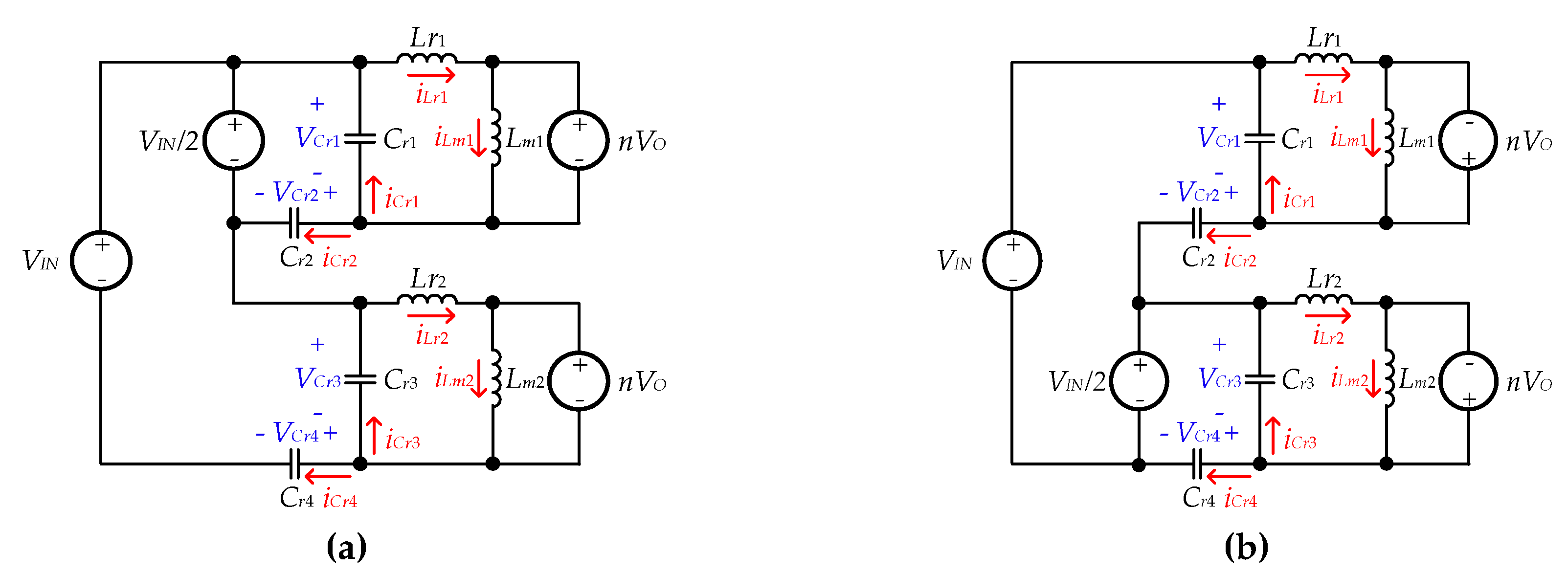
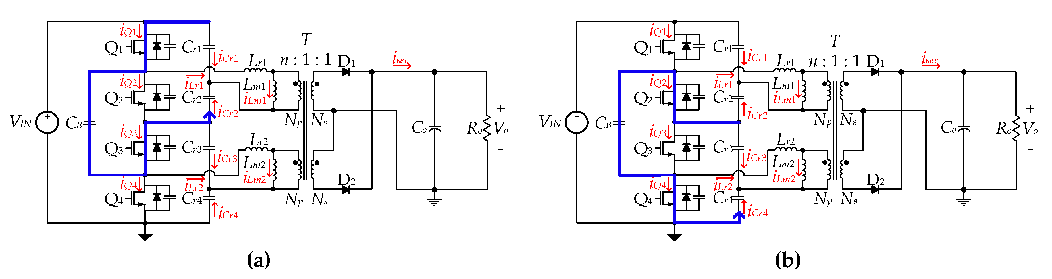
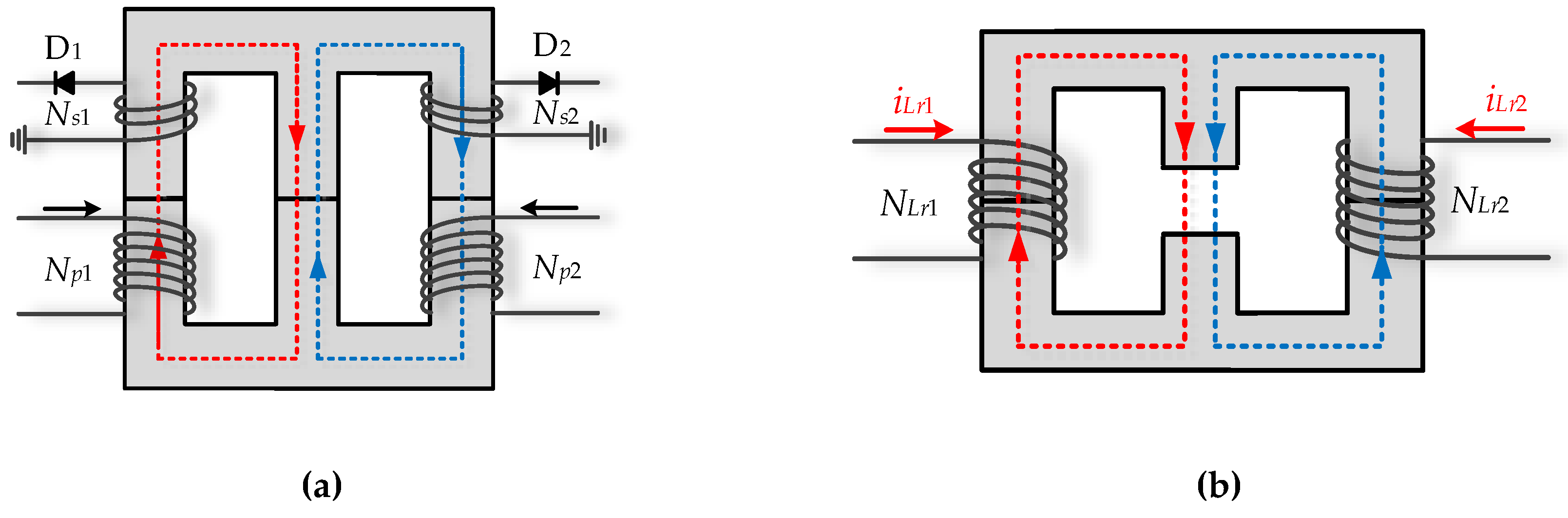
2. Operating Mode Analysis
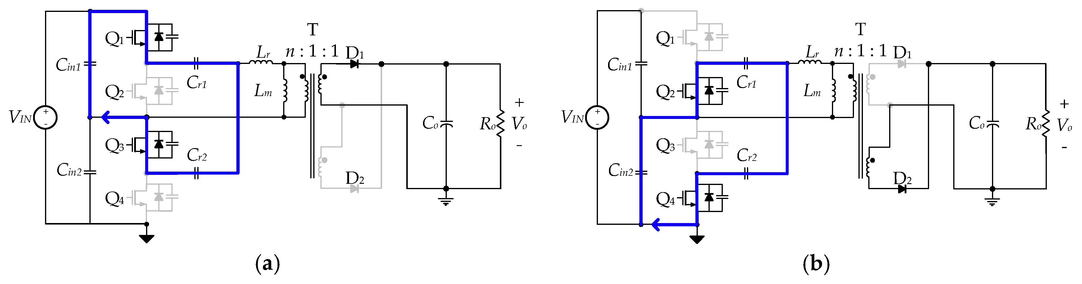
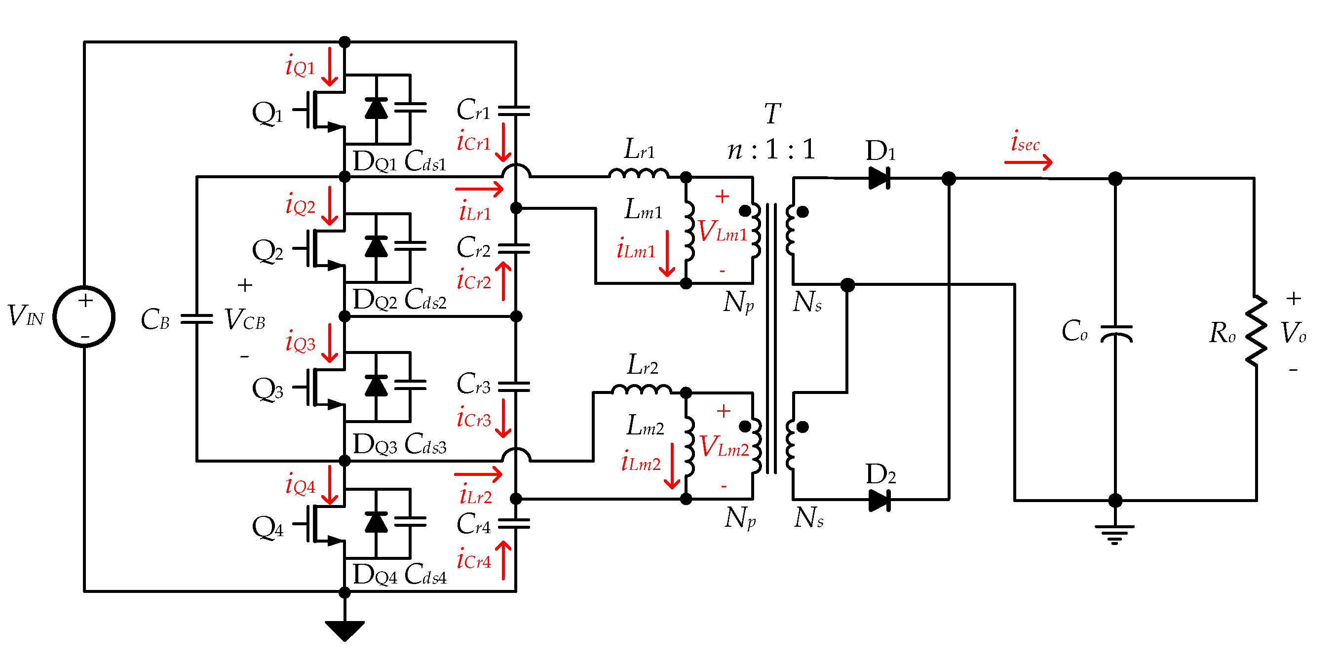
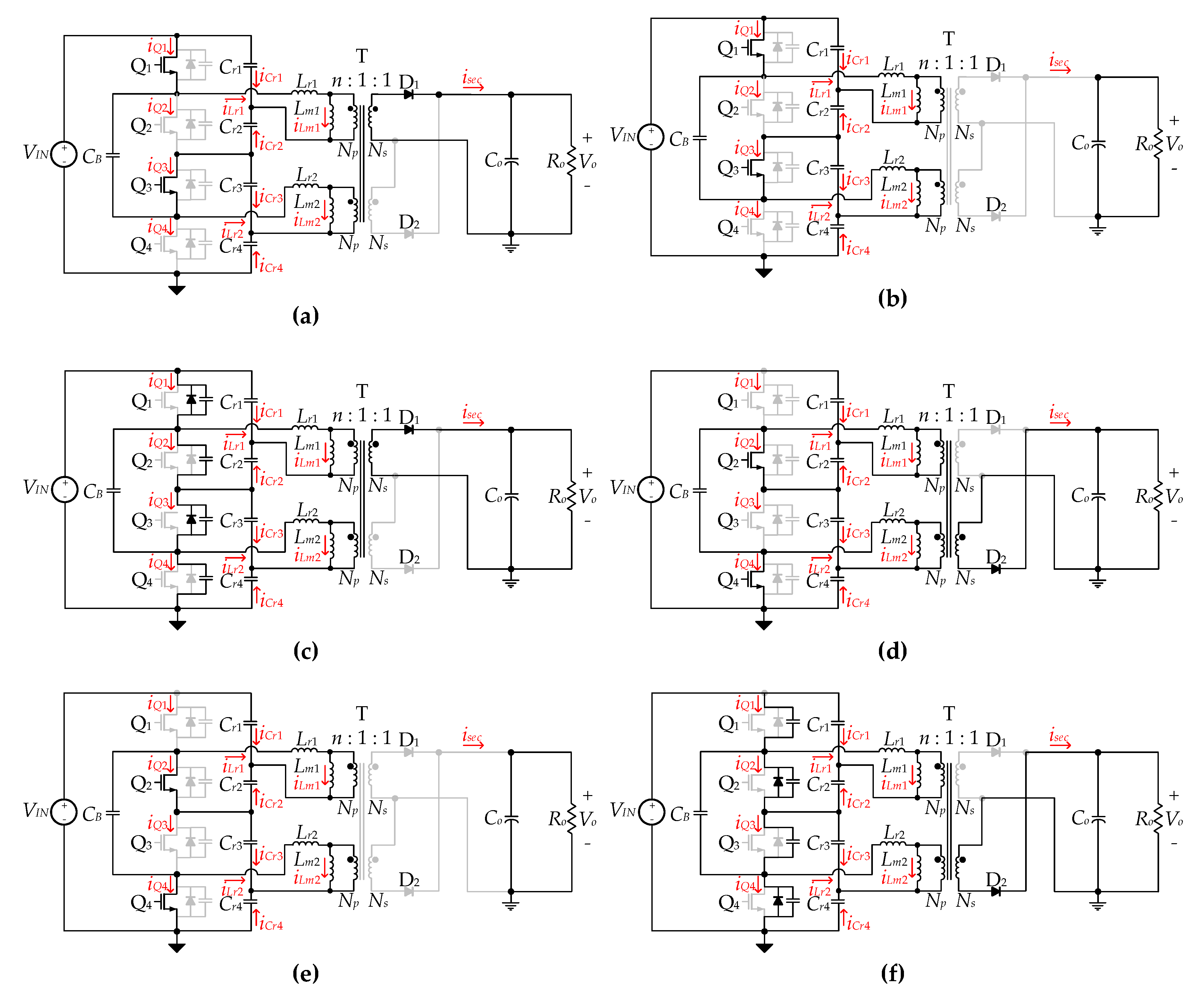
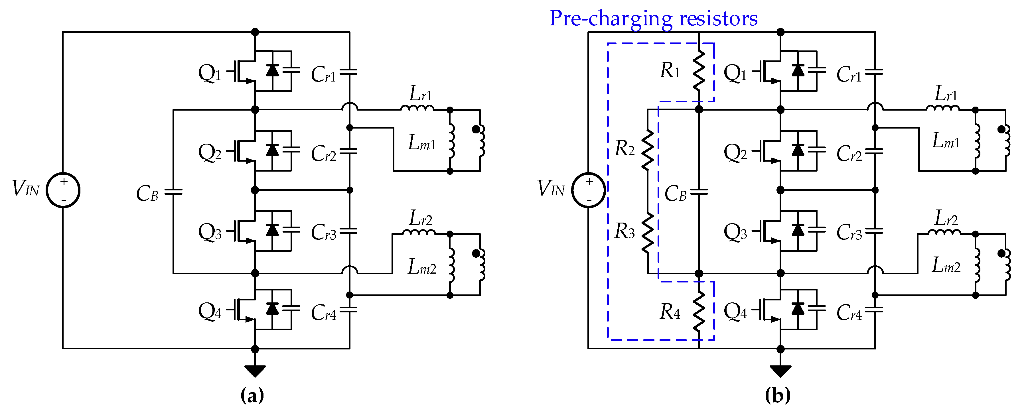
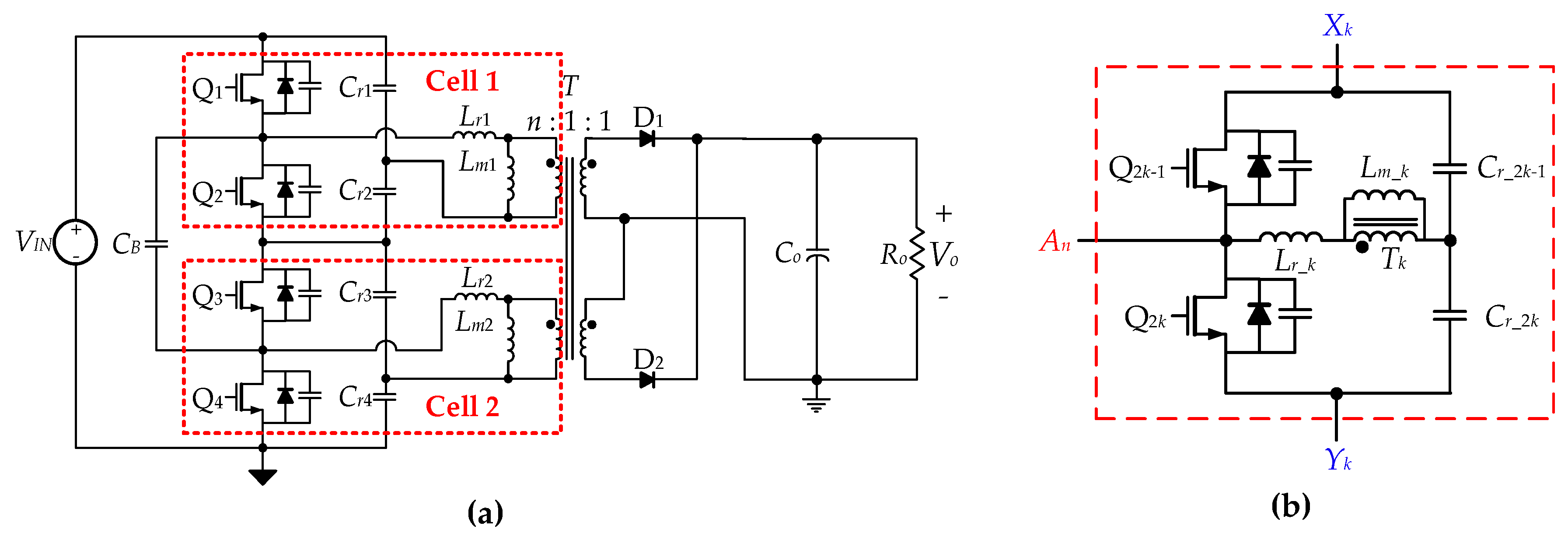
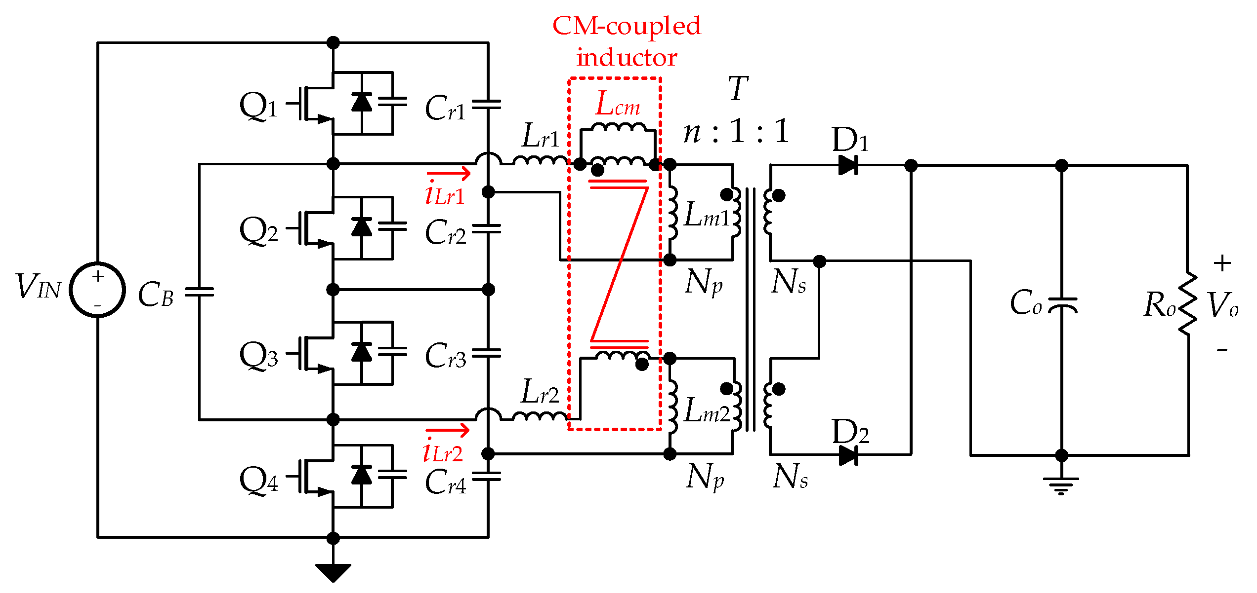
2.1. Circuit Operation
- Output capacitor CO is large enough to maintain a constant voltage.
- The four resonant capacitors, Cr1, Cr2, Cr3, and Cr4, have the same capacitance of Cr.
- The balancing capacitor CB is larger than the resonant capacitors (Cr1, Cr2, Cr3, and Cr4) to be considered as a voltage source of VIN/2.
- The output capacitance of all Si-FETs is the same as the capacitance of Cds.
- All Si-FETs and main switches have parasitic diodes of DQ1, DQ2, DQ3, and DQ4.
- The two resonant inductors, Lr1 and Lr2, have the same inductance Lr.
- The two magnetizing inductors, Lm1 and Lm2, have the same inductance Lm.
- The turn ratio of the main transformer T is n = Np/Ns.
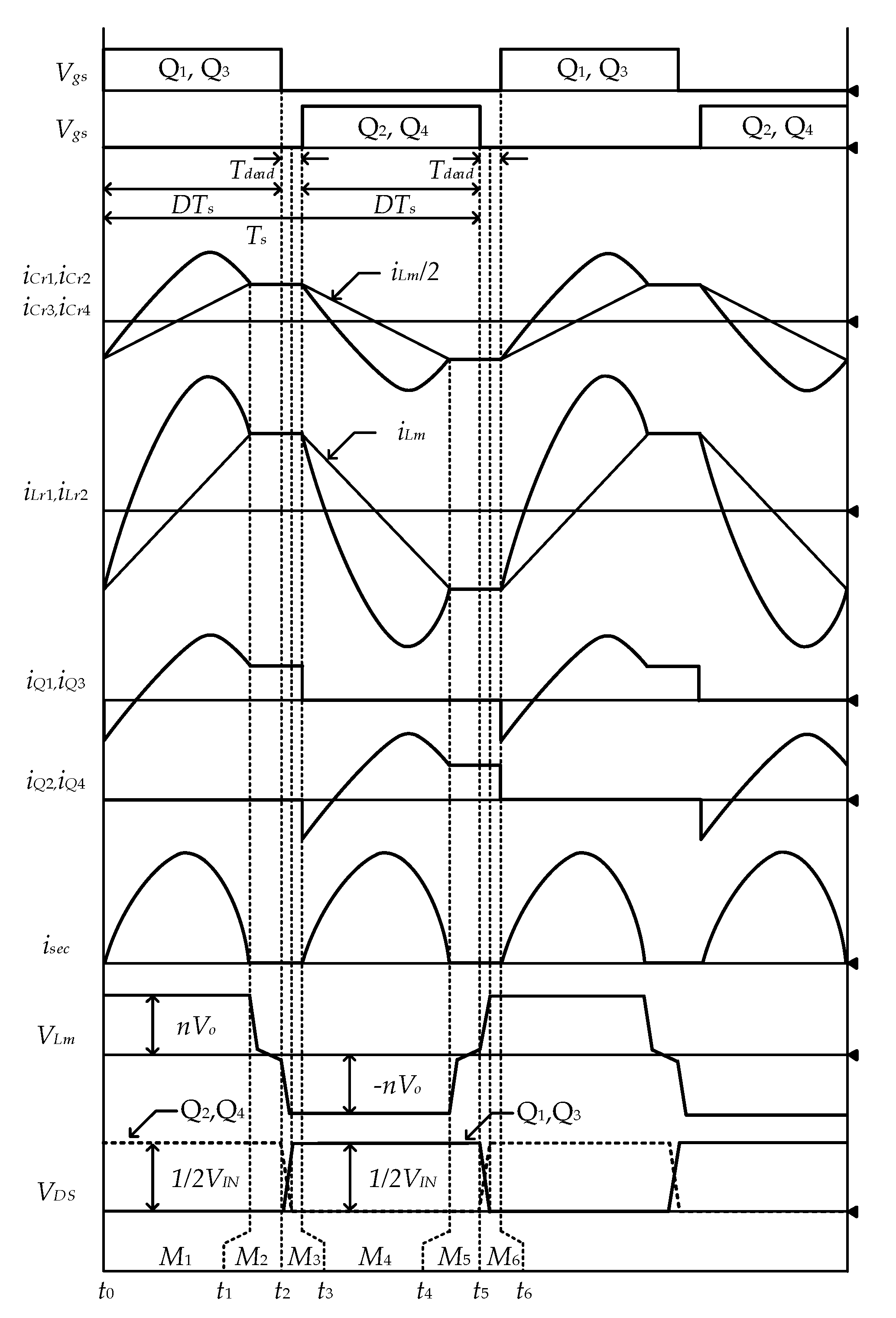
Circuit Operation in a Steady State
3. Analysis and Design Considerations
3.1. Principle of Voltage Balancing
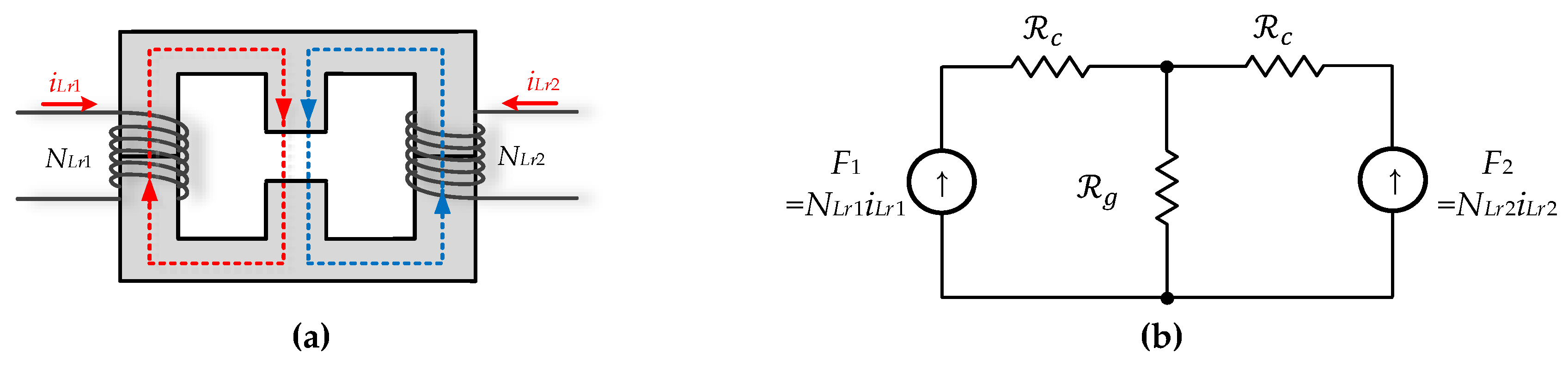
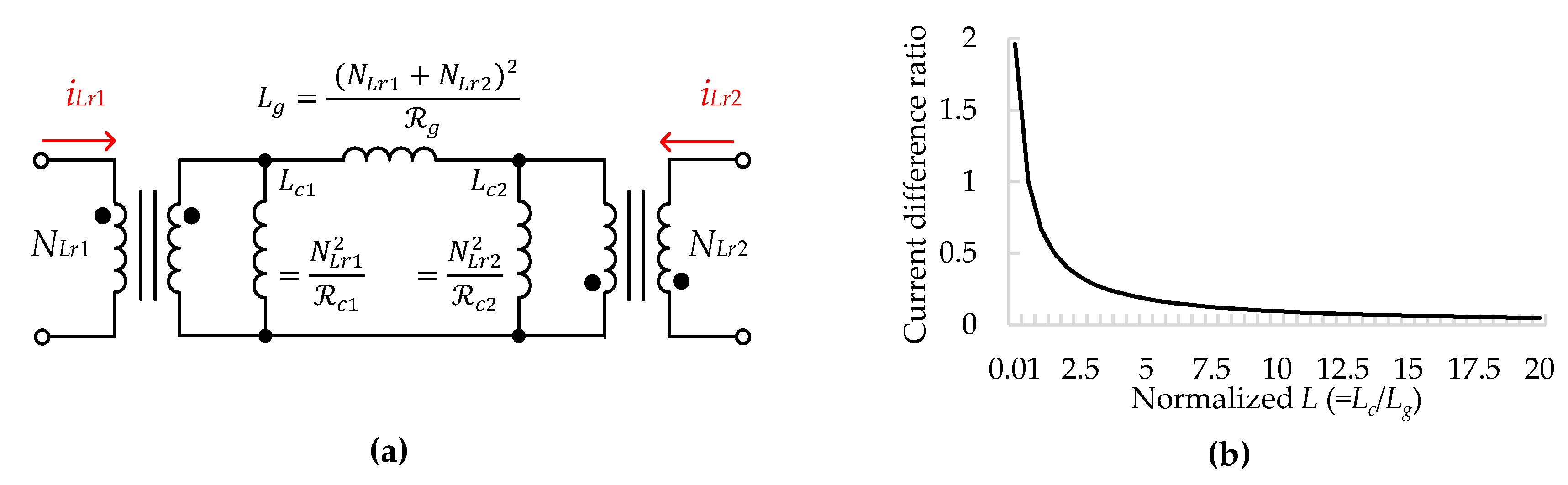
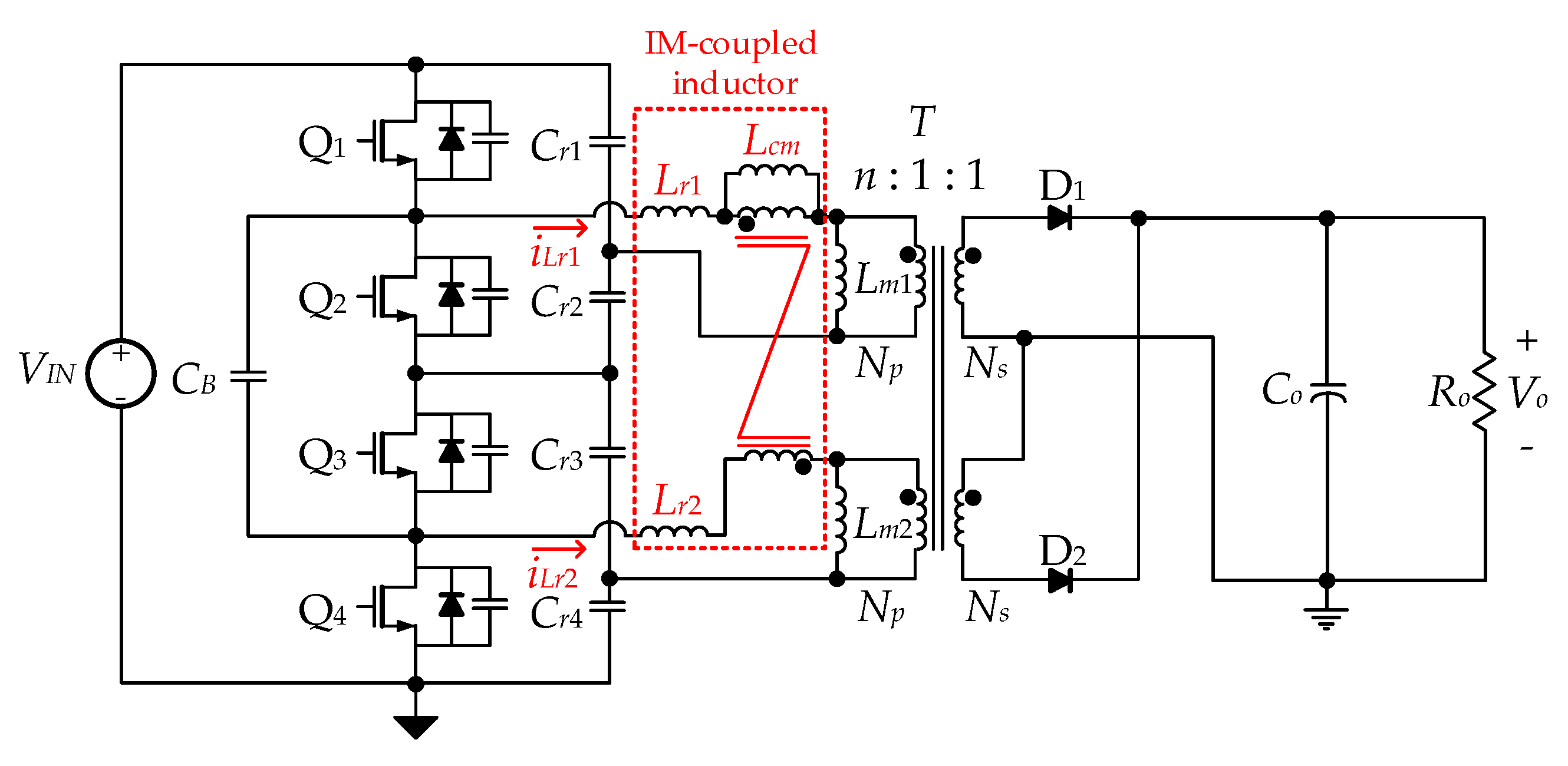
3.2. Principle of Current Balancing
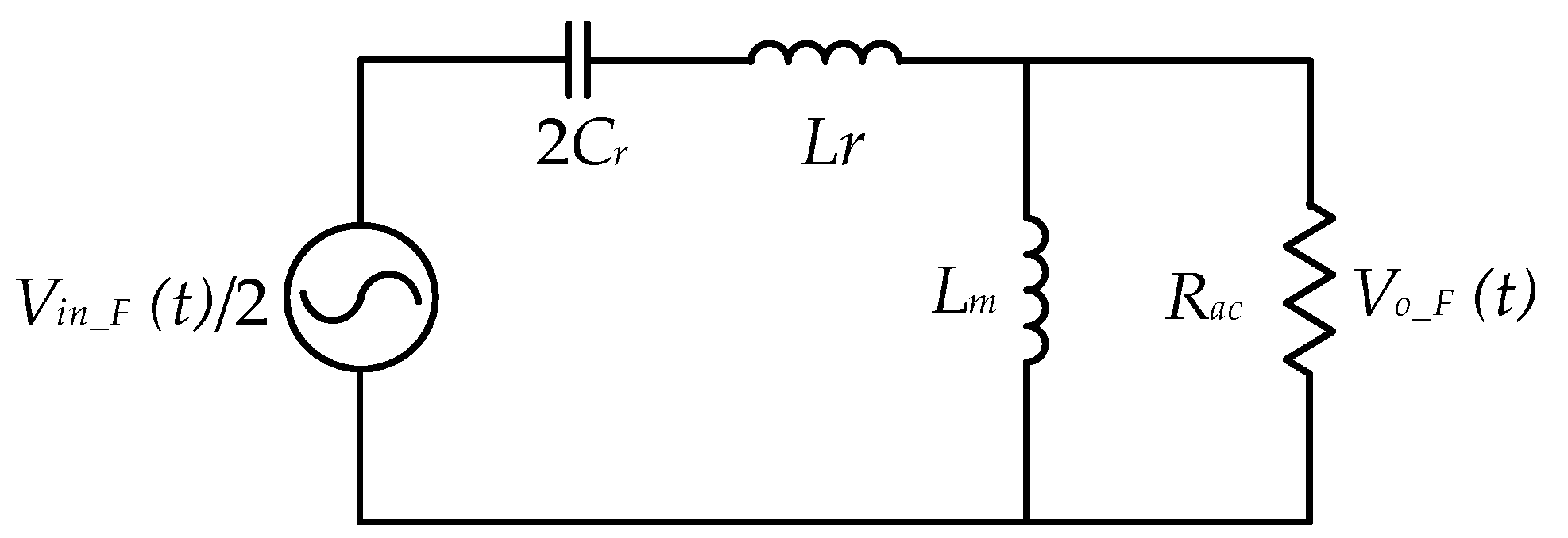
3.3. Voltage Conversion Ratio
- ,
- ,
- ,
- ,
- .
3.4. ZVS Condition
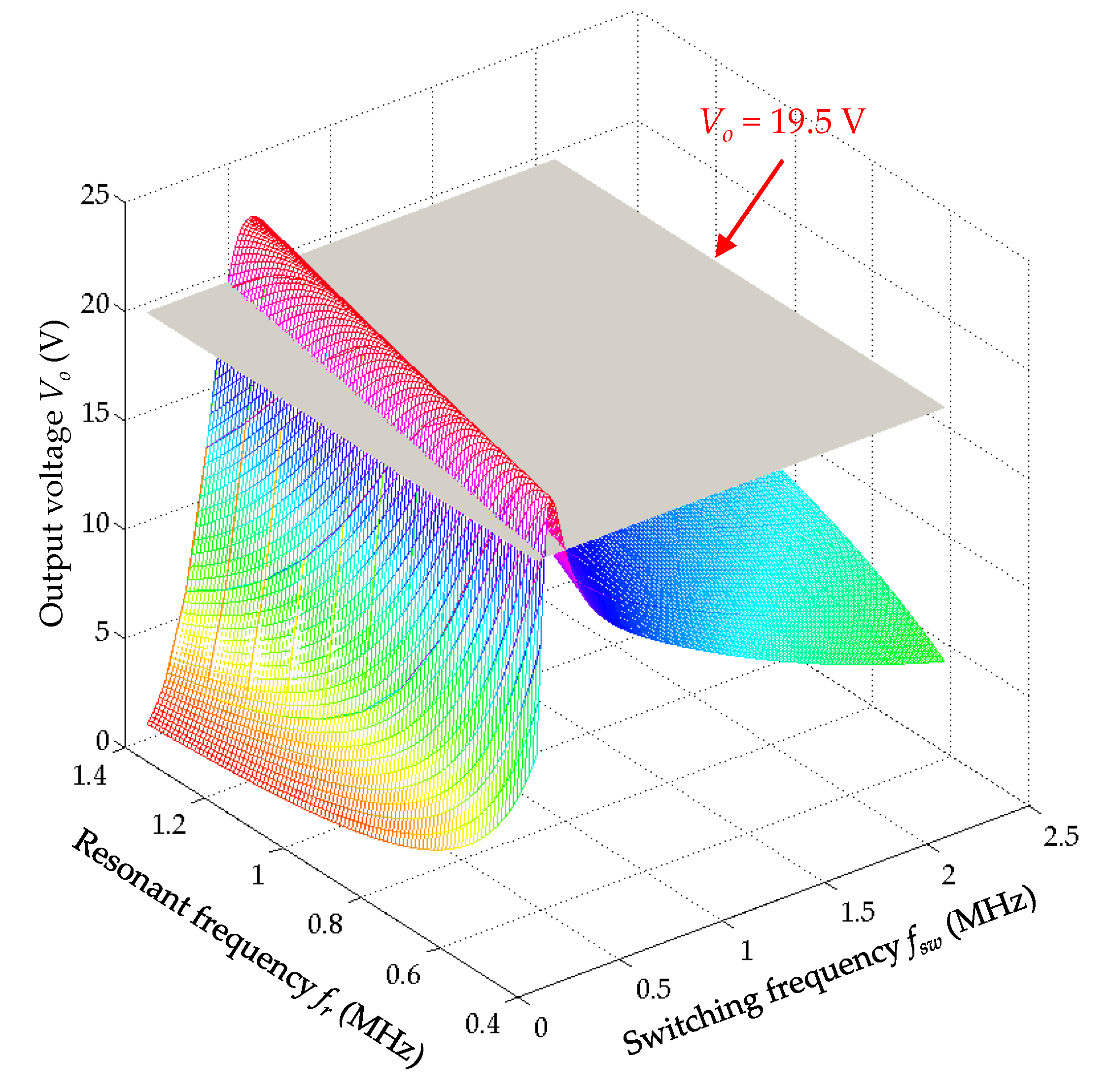
3.5. Maximum Gain Analysis
3.6. Comparison of Major Components
3.6.1. Stress Comparison
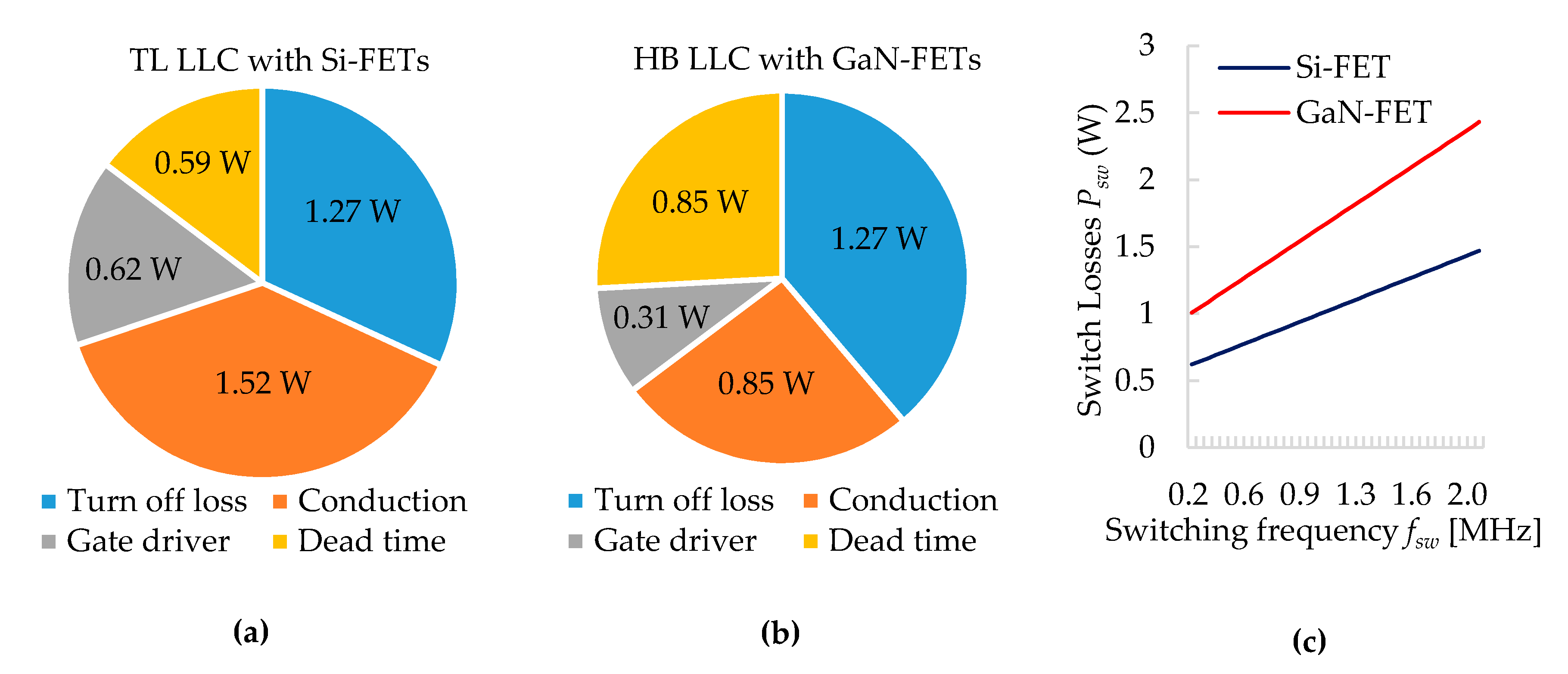
3.6.2. Comparison of Switch Loss
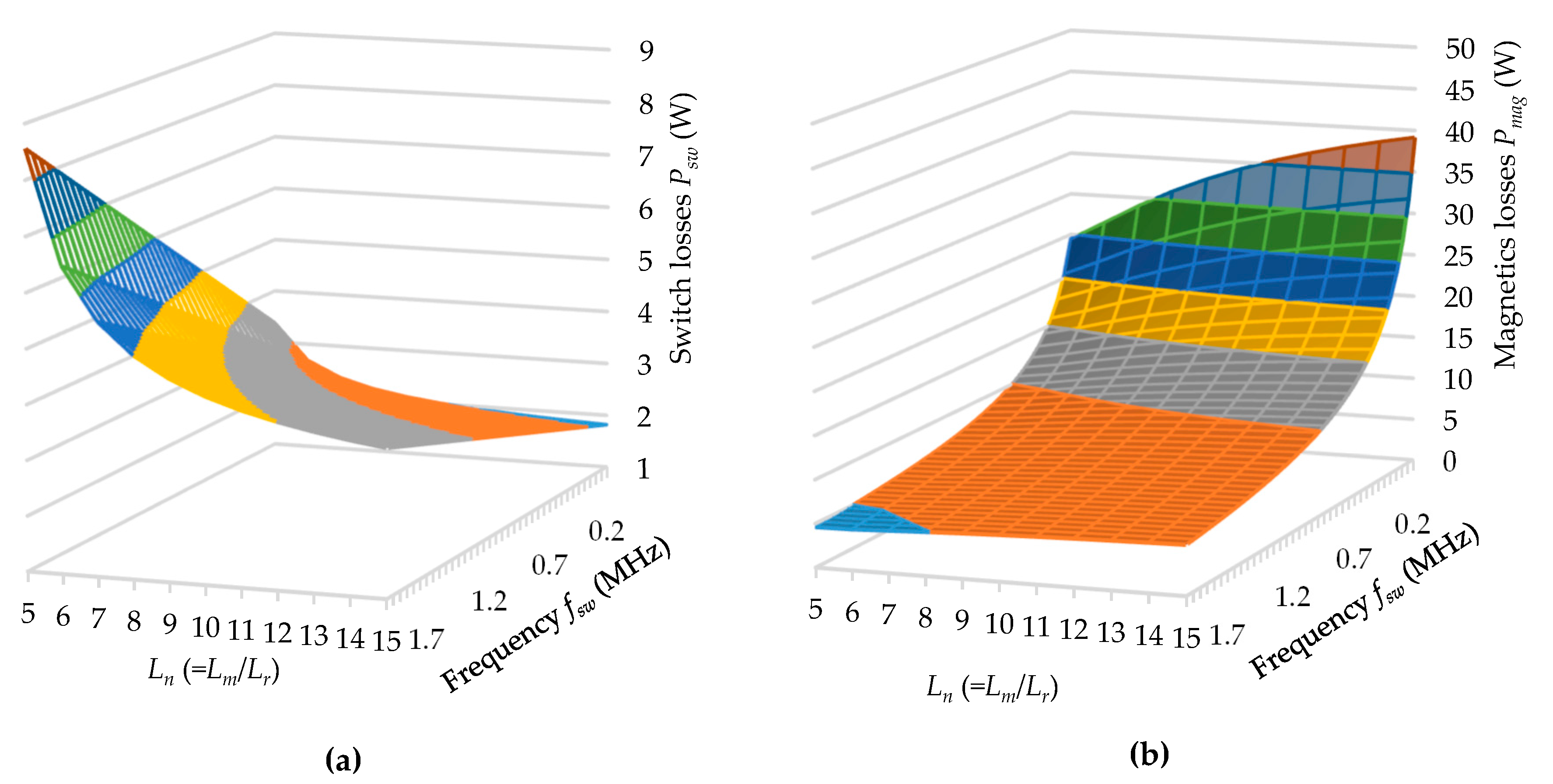
3.7. Optimal Design through the Loss Analysis
3.7.1. Loss Analysis for Switching Components
3.7.2. Loss Analysis for Magnetics
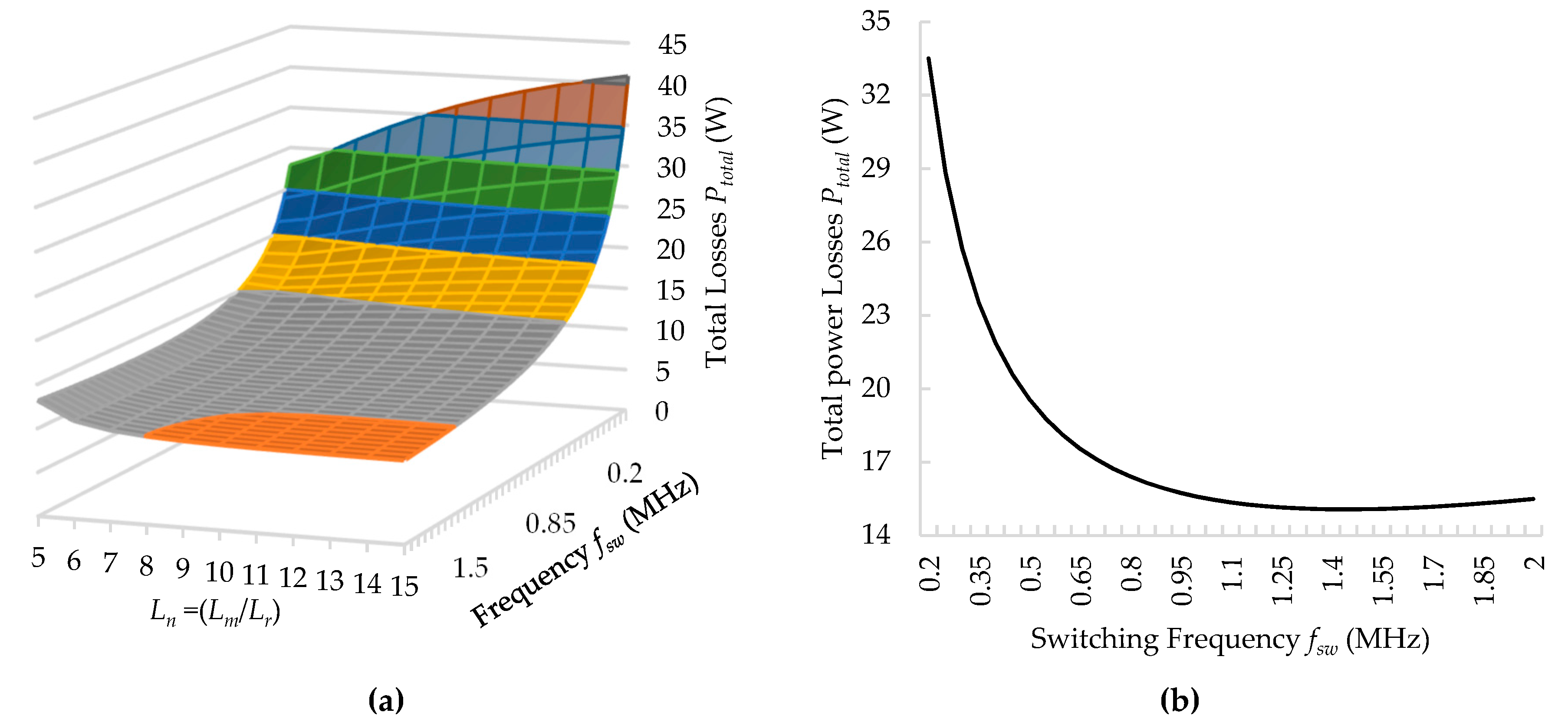
3.7.3. Results of Loss Analysis
- Input voltage: VIN = 390 V
- Output voltage: VO = 19.5 V
- Output power: PO = 350 W
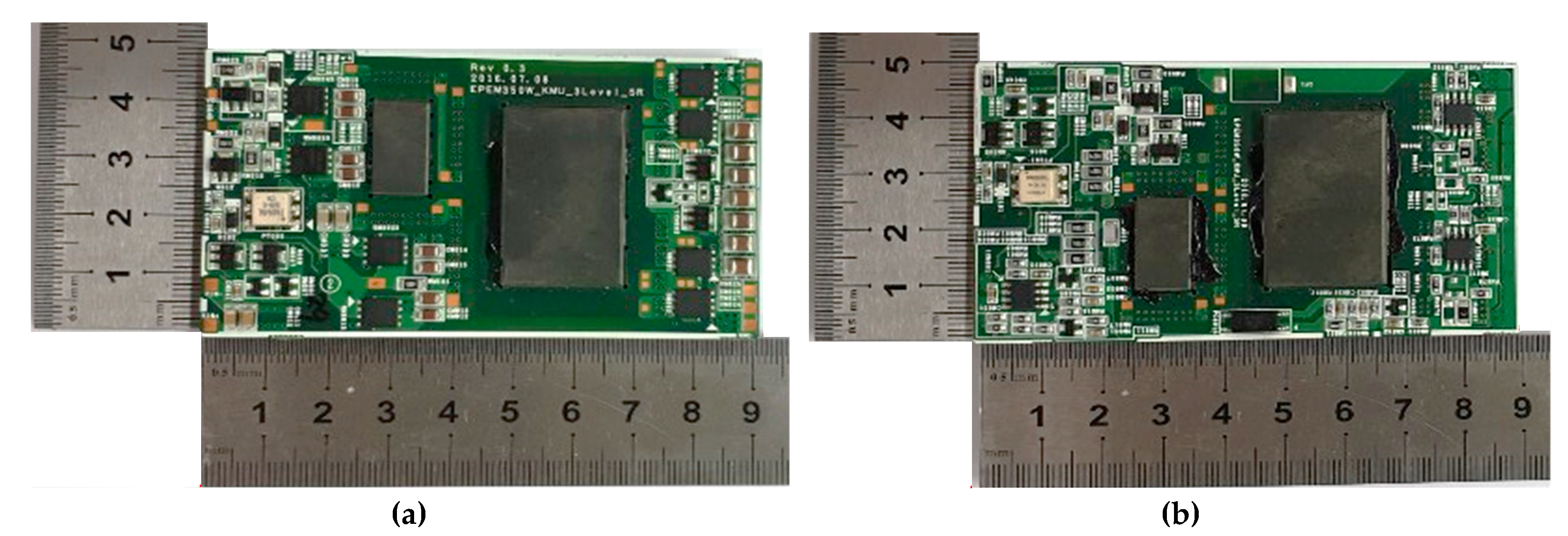
4. Experimental Results
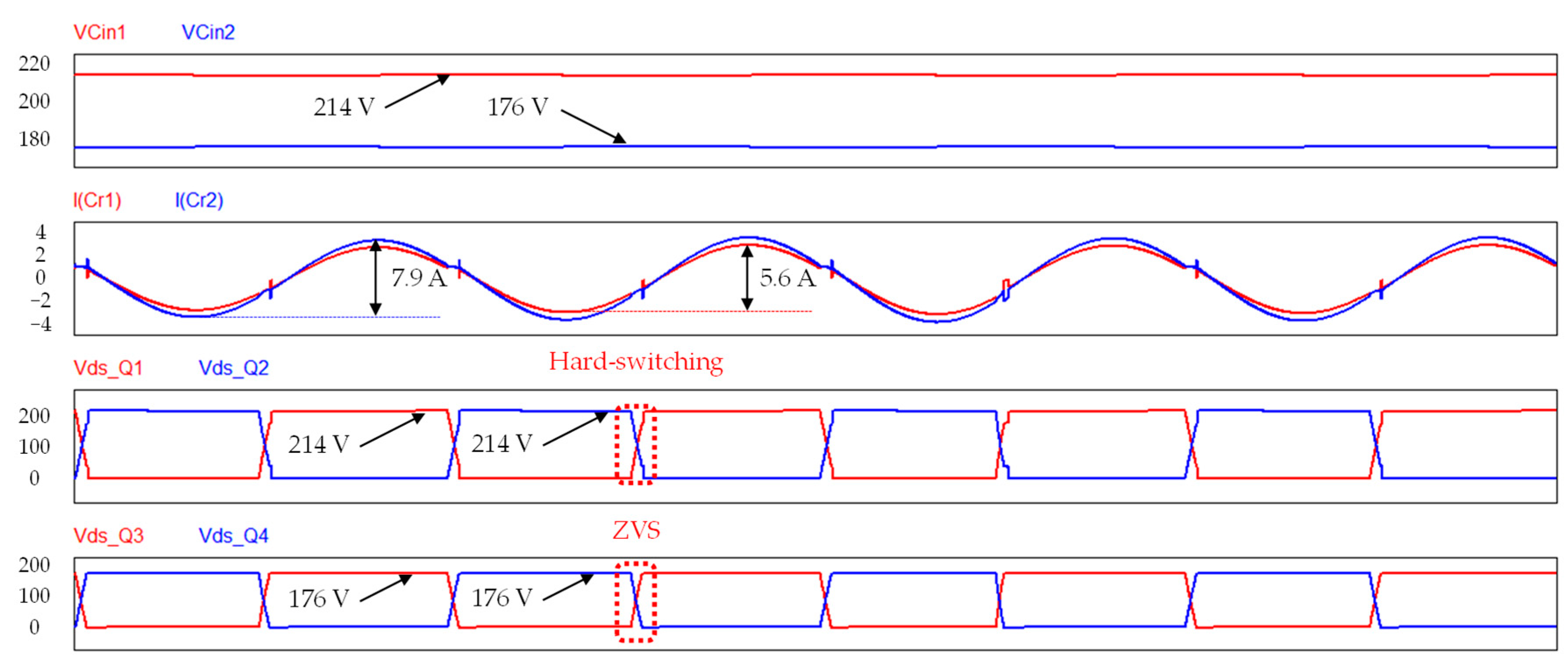
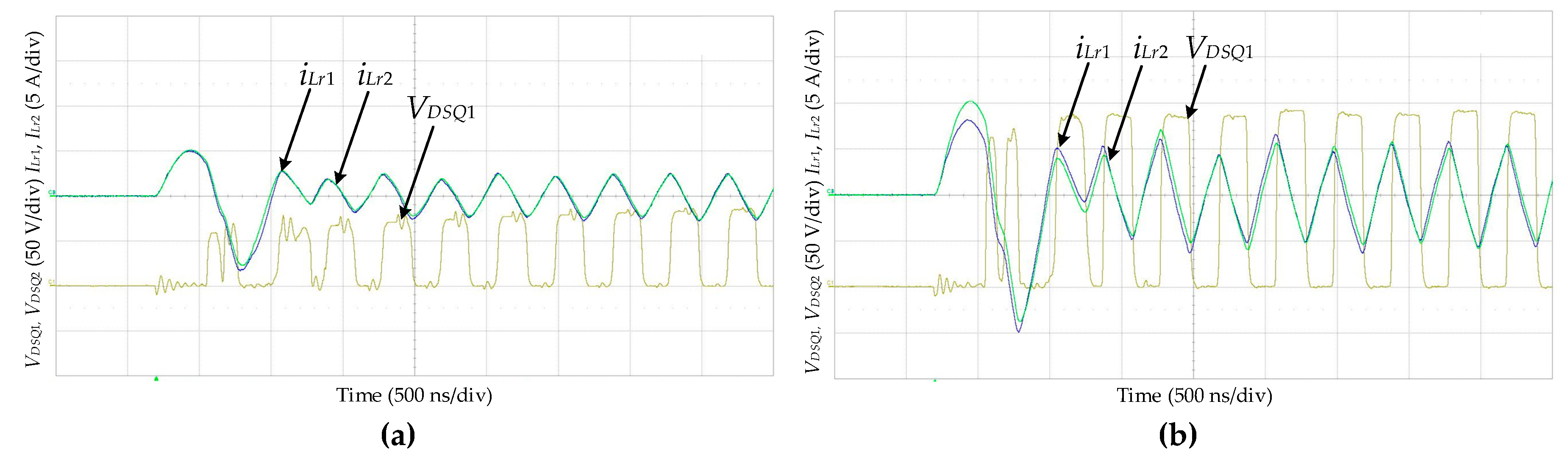
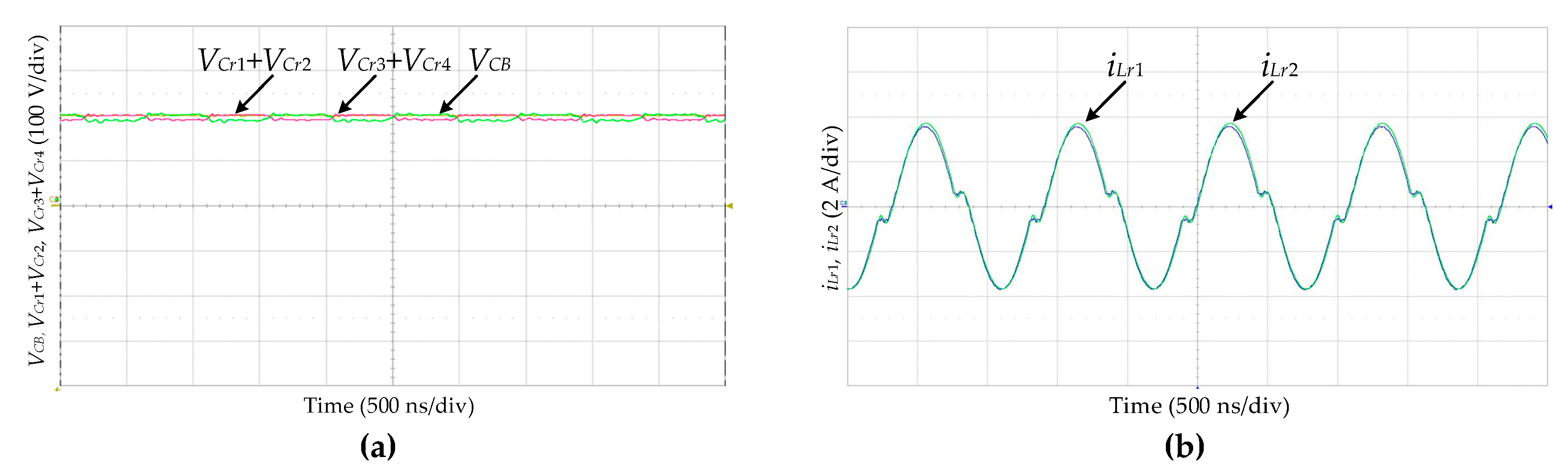
4.1. Practical Voltage Balancing under Soft Start-Up Conditions
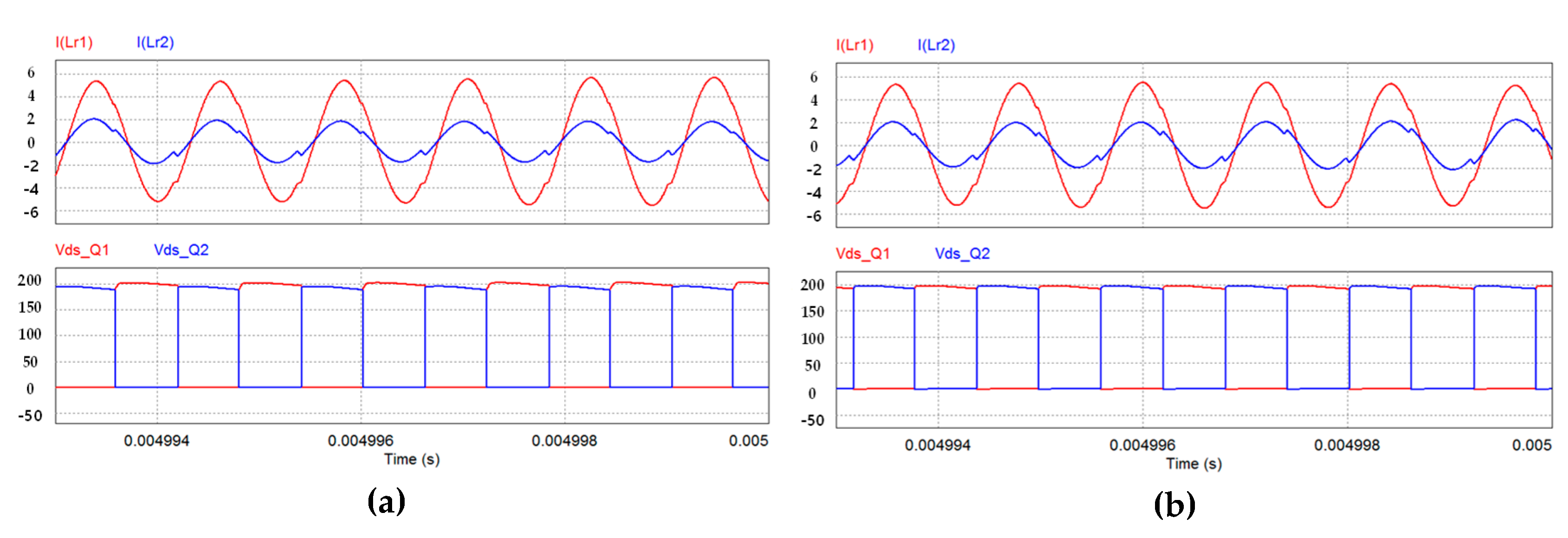
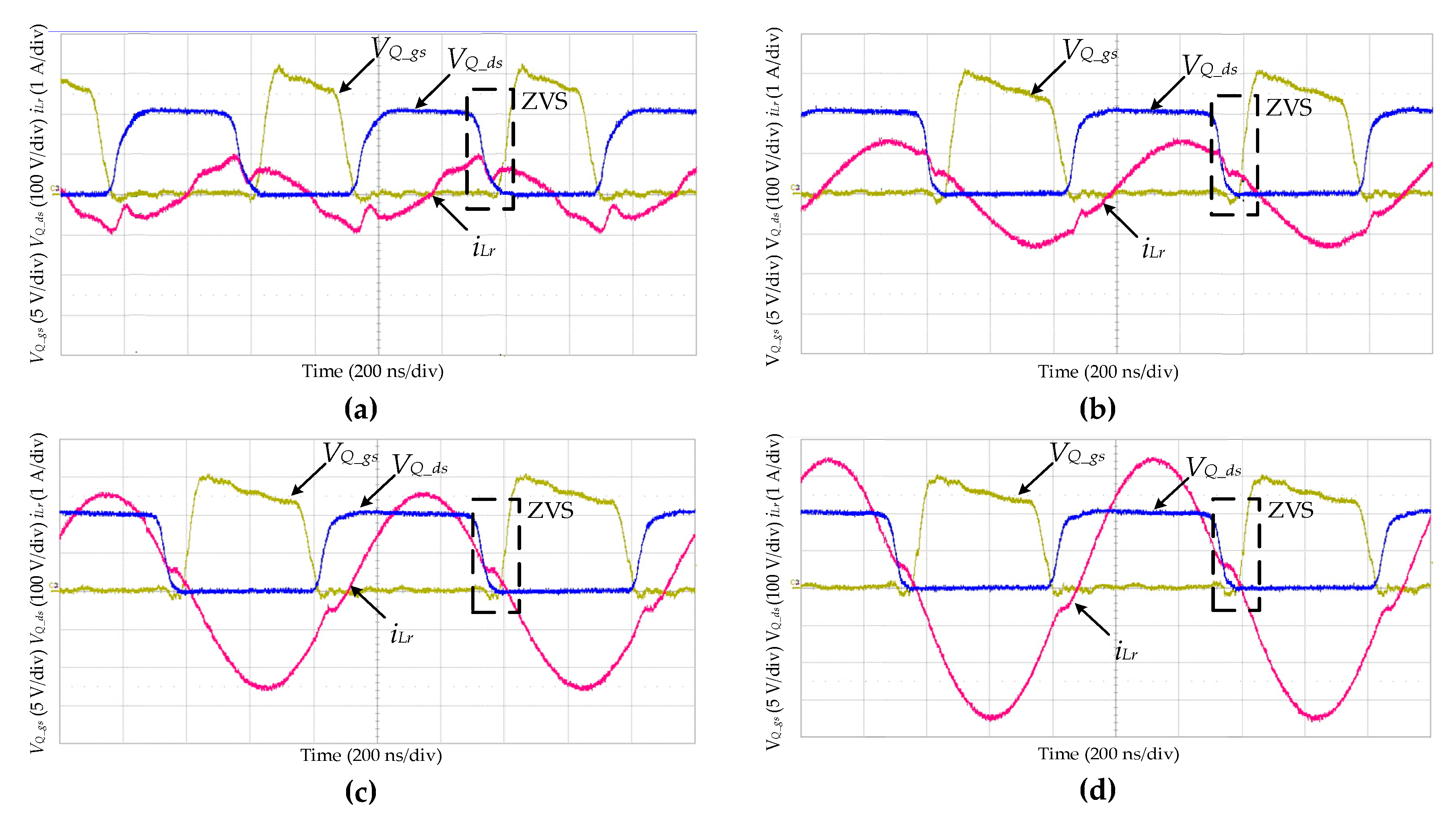
4.2. Waveforms
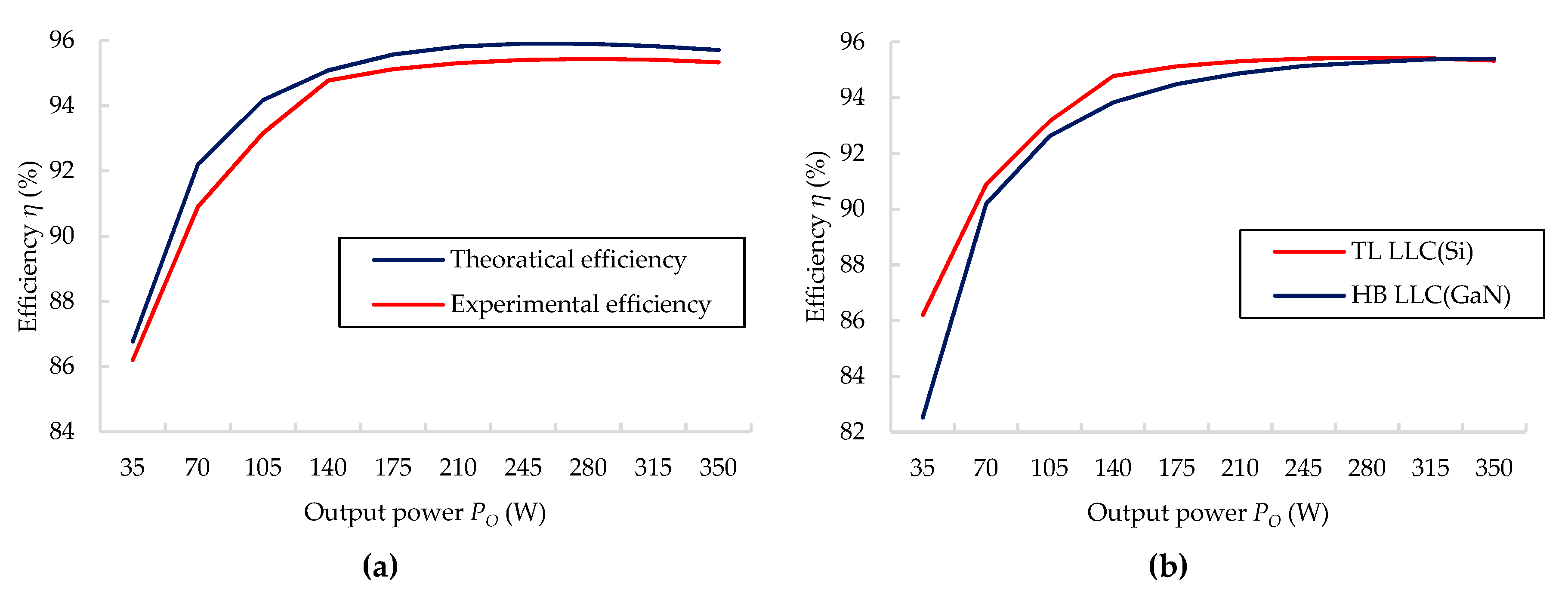
4.3. Efficiency
5. Conclusions
Author Contributions
Funding
Conflicts of Interest
References
- Duarte, C.M.; Fiori, V.M. A new ZVS-PWM active-clamping buck-boost converter. In Proceedings of the 2005 IEEE 36th Power Electronics Specialists Conference, Recife, Brazil, 12–16 June 2005. [Google Scholar]
- Zhang, Y.; Xu, D. Design and implementation of an accurately regulated multiple output ZVS DC–DC converter. IEEE Trans. Power Electron. 2007, 22, 1731–1742. [Google Scholar] [CrossRef]
- Mao, H.; Rahman, O.A.; Batarseh, I. Zero-voltage-switching DC–DC converters with synchronous rectifiers. IEEE Trans. Power Electron. 2008, 23, 369–378. [Google Scholar] [CrossRef]
- Das, P.; Laan, B.; Mousavi, S.A.; Moschopoulos, G. A nonisolated bidirectional ZVS-PWM active clamped DC–DC converter. IEEE Trans. Power Electron. 2009, 24, 553–558. [Google Scholar] [CrossRef]
- Das, P.; Mousavi, S.A.; Moschopoulos, G. Analysis and design of a nonisolated bidirectional ZVS-PWM DC–DC converter with coupled inductors. IEEE Trans. Power Electron. 2010, 25, 2630–2641. [Google Scholar] [CrossRef]
- Kim, I.D.; Paeng, S.H.; Ahn, J.W.; Nho, E.C.; Ko, J.S. New bidirectional ZVS PWM sepic/zeta DC-DC converter. In Proceedings of the 2007 IEEE International Symposium on Industrial Electronics, Vigo, Spain, 4–7 June 2007. [Google Scholar]
- Costa, D.B.; Duarte, C.M.C. The ZVS-PWM active-clamping CUK converter. IEEE Trans. Ind. Electron. 2004, 51, 54–60. [Google Scholar] [CrossRef]
- Yang, B.; Lee, F.C.; Zhang, A.J.; Huang, G. LLC resonant converter for front end DC/DC conversion. In Proceedings of the APEC Seventeenth Annual IEEE Applied Power Electronics Conference and Exposition, Dallas, TX, USA, 10–14 March 2002. [Google Scholar]
- Lu, B.; Liu, W.; Liang, Y.; Lee, F.C.; Van Wyk, J.D. Optimal design methodology for LLC resonant converter. In Proceedings of the Twenty-First Annual IEEE Applied Power Electronics Conference and Exposition, Dallas, TX, USA, 19–23 March 2006. [Google Scholar]
- Zhang, W.; Long, Y.; Zhang, Z.; Wang, F.; Tolbert, L.M.; Blalock, B.J.; Dean, R. Evaluation and comparison of silicon and gallium nitride power transistors in LLC resonant converter. In Proceedings of the 2012 IEEE Energy Conversion Congress and Exposition (ECCE), Raleigh, NC, USA, 15–20 September 2012. [Google Scholar]
- Kunihiro, K.; Kasahara, K.; Takahashi, Y.; Ohno, Y. Experimental evaluation of impact ionization coefficients in GaN. IEEE Electron. Device Lett. 1999, 20, 608–610. [Google Scholar]
- Zhang, W.; Xu, Z.; Zhang, Z.; Wang, F.; Tolbert, L.M.; Blalock, B.J. Evaluation of 600 V cascode GaN HEMT in device characterization and all-GaN-based LLC resonant converter. In Proceedings of the 2013 IEEE Energy Conversion Congress and Exposition, Denver, CO, USA, 15–19 September 2013. [Google Scholar]
- Huang, X.; Liu, Z.; Li, Q.; Lee, F.C. Evaluation and application of 600 V GaN HEMT in cascode structure. IEEE Trans. Power Electron. 2013, 29, 2453–2461. [Google Scholar] [CrossRef]
- Gu, Y.; Lu, Z.; Hang, L.; Qian, Z.; Huang, G. Three-level LLC series resonant DC/DC converter. IEEE Trans. Power Electron. 2005, 20, 781–789. [Google Scholar] [CrossRef]
- Canales, F.; Barbosa, P.; Lee, F.C. A wide input voltage and load output variations fixed-frequency ZVS DC/DC LLC resonant converter for high-power applications. In Proceedings of the Conference Record of the 2002 IEEE Industry Applications Conference, 37th IAS Annual Meeting, Pittsburgh, PA, USA, 13–18 October 2002. [Google Scholar]
- Canales, F.; Barbosa, P.M.; Burdio, J.M.; Lee, F.C. A zero voltage switching three-level DC/DC converter. In Proceedings of the Twenty-Second International Telecommunications Energy Conference, Phoenix, AZ, USA, 10–14 September 2000. [Google Scholar]
- Lee, I.O.; Moon, G.W. Analysis and design of a three-level LLC series resonant converter for high-and wide-input-voltage applications. IEEE Trans. Power Electron. 2011, 27, 2966–2979. [Google Scholar] [CrossRef]
- Strollo, A.G.; Napoli, E. Optimal ON-resistance versus breakdown voltage tradeoff in superjunction power devices: A novel analytical model. IEEE Trans. Electron. Devices 2011, 48, 2161–2167. [Google Scholar] [CrossRef]
- Shen, Z.J.; Xiong, Y.; Cheng, X.; Fu, Y.; Kumar, P. Power MOSFET switching loss analysis: A new insight. In Proceedings of the Conference Record of the 2006 IEEE Industry Applications Conference Forty-First IAS Annual Meeting, Tampa, FL, USA, 8–12 October 2006. [Google Scholar]
- Steinmetz, C.P. On the law of hysteresis. Proc. IEEE 1984, 72, 197–221. [Google Scholar] [CrossRef]
- Ayachit, A.; Kazimierczuk, M.K. Steinmetz equation for gapped magnetic cores. IEEE Magn. Lett. 2016, 7, 1–4. [Google Scholar] [CrossRef]


| Components | Symbols | Equations | |
|---|---|---|---|
| TL LLC Resonant Converter | HB LLC Resonant Converter | ||
| Si-FET | VQ_peak | ||
| Resonant capacitor | VCr_peak | ||
| Parameters | Value | Unit | |
|---|---|---|---|
| TL LLC Resonant Converter | HB LLC Resonant Converter | ||
| Input voltage VIN | 390 | VDC | |
| Output voltage VO | 19.5 | VDC | |
| Output power PO | 350 | W | |
| Gate-to-source voltage Vdrv | 15 | VDC | |
| SR Gate-to-source voltage VSR_drv | 10 | VDC | |
| Dead time tdead | 100 | ns | |
| Resonant capacitances Cr | 5.5 | 1.375 | nF |
| Resonant inductance Lr | 2.6 | 10.4 | uH |
| Magnetizing inductance Lm | 14.5 | 58 | uH |
| Turn ratio n | 5:5:1:1 | 10:1 | |
| Switching frequency fsw | 1 | MHz | |
| Parameters | Value | Unit | |
|---|---|---|---|
| BSC16DN25NS3 (Si-FET) | TPH3206PD (GaN-FET) | ||
| Drain‒source breakdown voltage | 250 | 600 | V |
| Continuous drain current | 10.9 | 17 | A |
| Drain‒source on-state resistance | 0.16 | 0.18 | ohm |
| Input capacitance | 920 | 760 | pF |
| Output capacitance | 59 | 44 | pF |
| Rise time | 4 | 4.5 | ns |
| Fall time | 4 | 4 | ns |
| Source‒drain diode forward voltage | 0.9 | 2.6 | V |
| Components | Symbols | Equations |
|---|---|---|
| Si-FET | ||
| Transformer | ||
| SR-FET |
| Components | Symbols | Equations |
|---|---|---|
| Resonant inductor | ||
| Transformer | ||
| Components | Name |
|---|---|
| Si-FETs Q1, Q2, Q3, Q4 | BSC16DN25NS3 |
| Output rectifier D1, D2 | BSC061N08NS5 |
| Controller | SEM3150 |
| Thickness of pattern | 2oz (=0.7 mm) |
| Planar resonant inductor core | EE 0909 (ML-91S) |
| Relative permeability | 900 |
| Turns | 5 |
| Air gap of center leg | 0.31 mm |
| Air gap of outer leg | 0.03 mm |
| Planar transformer core | EE 2012 (ML-91S) |
| Relative permeability | 900 |
| Primary turns | 5 |
| Secondary turns | 1 |
| Air gap of center leg | 0.55 mm |
© 2019 by the authors. Licensee MDPI, Basel, Switzerland. This article is an open access article distributed under the terms and conditions of the Creative Commons Attribution (CC BY) license (http://creativecommons.org/licenses/by/4.0/).
Share and Cite
Yang, J.-W.; Han, S.-K. A Si-FET-Based High Switching Frequency Three-Level LLC Resonant Converter. Energies 2019, 12, 3082. https://doi.org/10.3390/en12163082
Yang J-W, Han S-K. A Si-FET-Based High Switching Frequency Three-Level LLC Resonant Converter. Energies. 2019; 12(16):3082. https://doi.org/10.3390/en12163082
Chicago/Turabian StyleYang, Jung-Woo, and Sang-Kyoo Han. 2019. "A Si-FET-Based High Switching Frequency Three-Level LLC Resonant Converter" Energies 12, no. 16: 3082. https://doi.org/10.3390/en12163082
APA StyleYang, J.-W., & Han, S.-K. (2019). A Si-FET-Based High Switching Frequency Three-Level LLC Resonant Converter. Energies, 12(16), 3082. https://doi.org/10.3390/en12163082