Article

Modeling and Optimization of Dual Active Bridge DC-DC Converter with Dead-Time Effect under Triple-Phase-Shift Control

School of Control Science and Engineering, Shandong University, Jinan 250061, China
*
Author to whom correspondence should be addressed.
Energies 2019, 12(6), 973; https://doi.org/10.3390/en12060973
Submission received: 29 January 2019 / Revised: 6 March 2019 / Accepted: 7 March 2019 / Published: 13 March 2019
(This article belongs to the Special Issue Advanced in Resonant Converter and Dual Active Bridge Converter)

Abstract

:
Dead-time effect has become an apparent issue in high-switching-frequency high-power dual active bridge (DAB) DC-DC converter. This paper gives a detailed analysis of phase-shift errors effect caused by dead time, including output voltage offset, soft-switching failure, optimal scheme failure, etc. Phase-shift errors effect will invalidate traditional analyses of optimal control and mislead the design of DAB converter. To overcome these drawbacks, various operating modes and an accurate transmission power model incorporating dead time under triple-phase-shift (TPS) control are developed. On this basis, an optimal TPS incorporating dead time (TPSiDT) scheme is further proposed to minimize the current stress, while guaranteeing soft-switching operation by using Lagrange multiplier method (LMM) and Genetic Algorithm (GA). The novel transmission power model can provide accurate power flow computation to avoid phase-shift errors. Therefore, in practical applications, the minimum current stress and soft-switching operation can be guaranteed, and the efficiency of DAB converter can be improved. Finally, the experimental results verify the feasibility of the proposed TPSiDT scheme.

1. Introduction

With the development of hybrid microgrid, battery energy storage systems, and uninterrupted power supplies, bidirectional DC-DC converters have been widely used in bidirectional power conversion applications [1,2,3,4,5]. Thereinto, dual active bridge (DAB) DC-DC converter gains more and more attention due to the advantages of high power density, soft-switching ability, bidirectional power-transfer capability, and high efficiency [6,7,8,9]. 
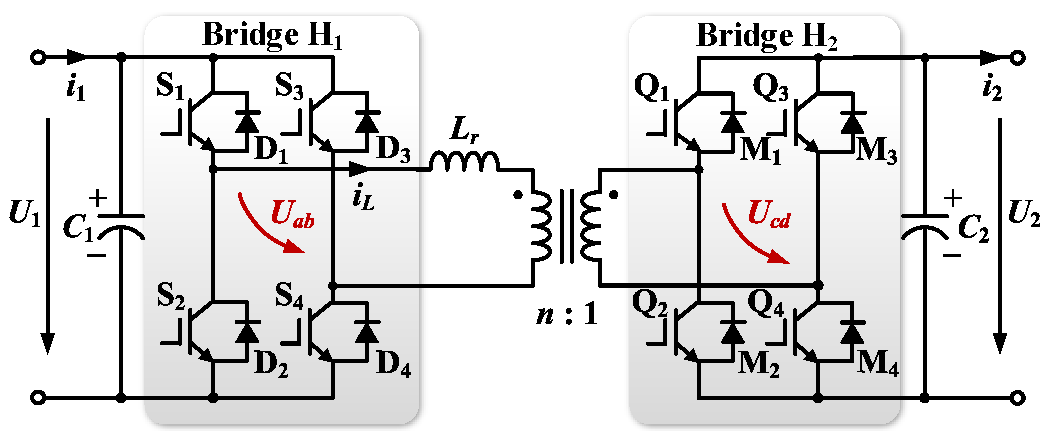
Figure 1 depicts the typical topology of DAB converter, which is constructed by two full bridges and a high-frequency isolated transformer with the turns ratio n:1. U ab and U cd are ac output voltages of two bridges H 1 and H 2 , respectively. L r is the sum of the transformer leakage inductance and the auxiliary inductor, and i L is the current of L r .
The basic control scheme of DAB converter is single-phase-shift (SPS) scheme, in which the direction and magnitude of the transmission power are merely determined by the outer phase-shift ratio between H 1 and H 2 . However, when the input and output voltages of the isolated transformer are mismatched, the converter will suffer from limited soft-switching range and high current stress, thus the efficiency will degrade significantly [10]. To improve the performance of the converter, enhanced-phase-shift (EPS) scheme, double-phase-shift (DPS) scheme and triple-phase-shift (TPS) scheme are proposed, which can increase the control freedom by adding inner phase-shift ratios inside H 1 and H 2 . Compared with other phase-shift schemes, TPS scheme facilitates the most degrees of control freedom, which controls the duty ratios of H 1 and H 2 by two extra inner phase-shift ratios individually. Therefore, TPS control has become the most popular phase-shift control scheme of DAB converter in current research [11,12].
Numerous modulation strategies have been proposed to improve the performance of DAB converter. These strategies mainly focus on minimizing current stress or root-mean-square (RMS) current [12,13], reducing backflow power [14,15], and broadening soft-switching range [16,17]. An optimal modulation scheme for minimizing the current stress of DAB converter under TPS control is proposed in [13]. Based on the relationship among the phase-shift ratios of the optimization algorithm, the optimal scheme can be realized without additional load-current sensor, and the complexity of the control system can be decreased. A unified triple-phase-shift (UTPS) scheme developed in [11] operates the converter in minimum-current-stress state while satisfying soft-switching constraints over the whole operation range. Therefore, the conducting losses, as well as the switching losses can be reduced, and the system efficiency can be improved. Unfortunately, all modulation schemes mentioned before fail to consider the existence of dead time, which is necessary to guarantee the system safety in practical applications.
To avoid shoot-through phenomenon and guarantee the reliability of the converter, dead time is necessary to be inserted between the interlocked switches in the same bridge. In traditional unidirectional DC-DC converter, the dead-time effect is usually ignored due to the limited dead-time ratio and low power rating. However, in high-power high-switching-frequency DAB converter, the dead-time ratio will be relatively larger, and the switching characterization, as well as the transmission power model, will be affected by dead time apparently [18,19]. The external characteristics caused by dead time are analyzed in detail under SPS and DPS control in [20,21], including voltage polarity reversal, voltage sag, duty-cycle abnormity, etc. Due to the voltage distortions, the ideal transmission power models in traditional schemes will be inaccurate, and have apparent deviation with the actual power models. The direct impact of the inaccurate power model is the phase-shift errors, which are defined as the differences between the phase-shift ratios calculated by the power model and the actual values to realize the required transmission power [18]. Various problems will result from phase-shift errors, such as output voltage offset, soft-switching failure, optimal scheme failure, etc. However, in previous work, researchers have paid more attention to the external characteristics of dead-time effect, and the phase-shift errors effect is seldom studied comprehensively. Actually, these problems will affect the accuracy of the traditional optimal schemes, and even invalidate the modulation schemes. Therefore, the performance of DAB converter will be degraded significantly.
In traditional inverters, dead-time compensation is a prevalent measure to deal with the voltage distortions and avoid the phase-shift errors. However, in DAB converter, the polarity of the current i L is changeable during the dead time, which brings challenges for detecting the current direction. Therefore, dead-time compensation is rather difficult to be applied in DAB converter [18]. To overcome the drawbacks of phase-shift errors caused by dead time, novel accurate power models incorporating dead time are developed in some studies. The authors of [20] focused on building a comprehensive transmission power model with dead-time effect under all voltage conversion ratio. In [22], a novel power model is developed over a short time scale incorporating dead time and semiconductor voltage loss. The transmission power and switching characteristics are provided in [19] to describe the dead-time effect in three-phase DAB converter. These accurate power models provide approaches for accurate power flow computation to avoid phase-shift errors. However, these previous studies remain in building the accurate power models, and further work, such as modulation scheme incorporating dead time is seldom studied. Based on the power model proposed in [20], an adaptive-dead-time scheme is developed to minimize the current stress in [23]. However, the minimum safe value of dead time is not considered, making the converter insecure in practical operation. Note that all the accurate transmission power models mentioned above are merely based on SPS control, and no modulation scheme incorporating dead time under TPS control is found at present.
In view of the study situation mentioned above, this paper proposes an optimal TPS incorporating dead time (TPSiDT) scheme for DAB converter. Due to the accurate power model proposed in this paper, the phase-shift errors can be avoided, and the converter can operate in minimum-current-stress and soft-switching state in practical applications. The rest of this paper is organized as follows. Section 2 analyzes the problems caused by phase-shift errors in detail. In Section 3, thirteen operating modes are compartmentalized under soft-switching constraints, and then, the accurate transmission power model and current stress model incorporating dead time are built. Section 4 presents the proposed TPSiDT scheme obtained by using Lagrange multiplier method (LMM) and Genetic Algorithm (GA). In Section 5, the accuracy of the power model and the effectiveness of TPSiDT scheme are verified by the experimental results. The conclusion is drawn in Section 6.

2. Phase-Shift Errors Effect of DAB Converter

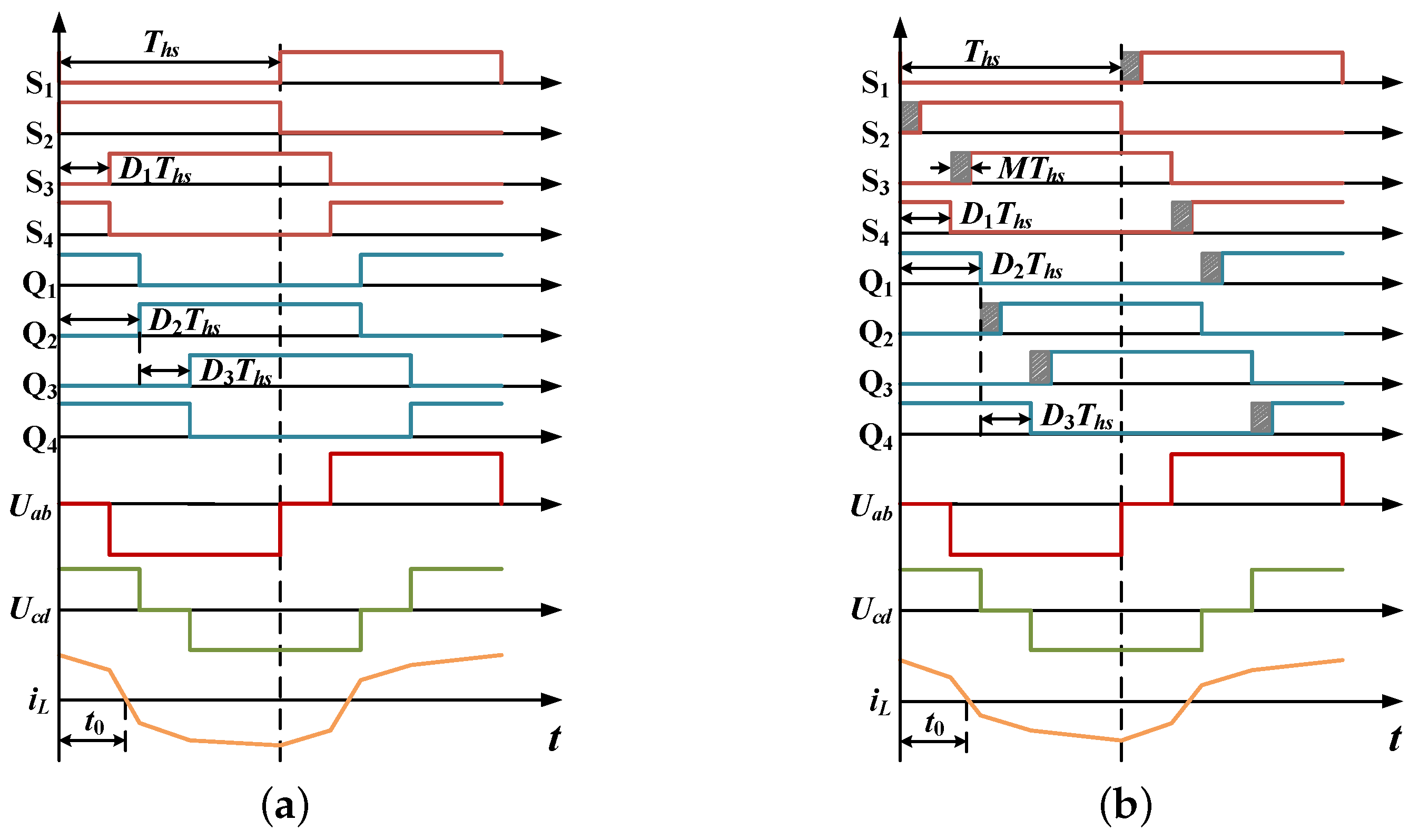
Figure 2 depicts the typical operating waveforms of DAB converter under ideal TPS control and actual TPS control, respectively. The ideal TPS control takes no account of dead time, and the magnitude of the power flow is determined by three phase-shift ratios. D 2 is the inner phase-shift ratio between S 1 and Q 1 . D 1 and D 3 are outer phase-shift ratios between S 1 and S 4 , and Q 1 and Q 4 , respectively. The value ranges of three phase-shift ratios are 0 D 1 , D 2 , amd D 3 1. However, in actual TPS control scheme, the dead-time ratio M becomes another factor to affect the transmission power of DAB converter, which presents the equivalent duty ratio of dead time in a half switching cycle. In Figure 2, T hs presents a half switching cycle, t 0 presents the zero-crossing point of i L , and T 0 = t 0 / T hs presents the zero-crossing-point ratio of i L . For convenience, the initial time of turn-off signal for S 1 is defined as beginning of the switching cycle.
The average transmission power of DAB converter can be calculated as
P = 1 T h s 0 T h s U a b ( t ) i L ( t ) d t
which indicates that the transmission power model is relevant to the waveforms of U ab and i L directly. Therefore, the voltage distortions caused by dead time will affect the traditional transmission power model and make it inaccurate. The inaccurate transmission power model will result in phase-shift errors, which will mislead the power calculation and design of DAB converter. The detailed analysis of the problems caused by phase-shift errors are described as follows.
(a) Output voltage offset: 
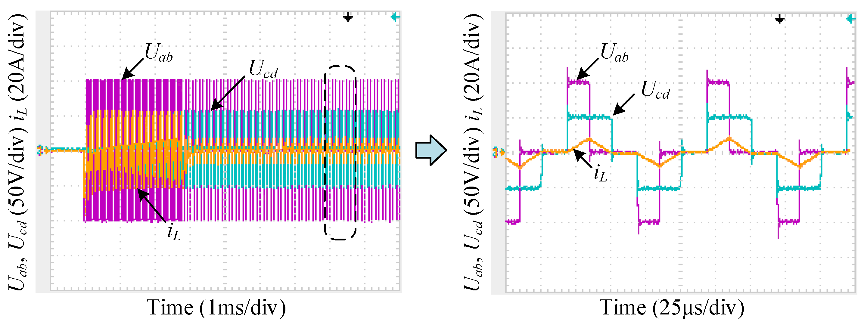
Figure 3 shows the transient waveforms switching from ideal TPS control to actual TPS control in open-loop system, in which the input voltage is 100 V, the transmission power is 125 W, the transformer turns ratio is 1, and the required output voltage is set to 50 V. From the waveform of the output voltage as shown in Figure 3a, it can be seen that in ideal operation, the dead-time ratio M is set to zero, and the output voltage U 2 is 50 V, which is identical with the required value. However, when M is set to 0.1 at 0.2 s, the output voltage falls to 37.5 V, and there is a significant offset between the two voltages. The corresponding waveform of the inductor current is shown in Figure 3b, in which the current decreases obviously at the switching point. Thus, the transmission power will decrease when considering the dead time, which coincides with Figure 3a. It indicates that, in practical operation, the theoretical phase-shift ratios calculated by ideal power model cannot realize the required transmission power.
(b) Soft-switching failure: In practical applications, the converter generally operates in closed-loop schemes to guarantee the system stability. For instance, in the UTPS scheme proposed in [11], D 1 and D 3 are calculated by the optimization algorithm, and D 2 is regulated by PI controller to obtain the required transmission power. To compensate the output voltage offset caused by phase-shift errors, the outer phase shift regulated by PI controller will be significantly different from the theoretical value. Therefore, soft-switching constraints of DAB converter may not be satisfied in practical operation. 
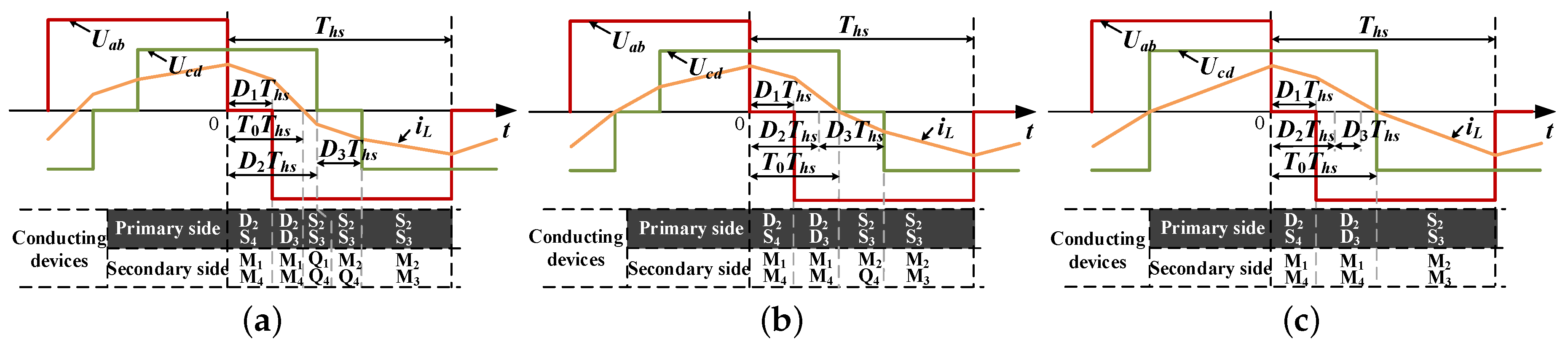
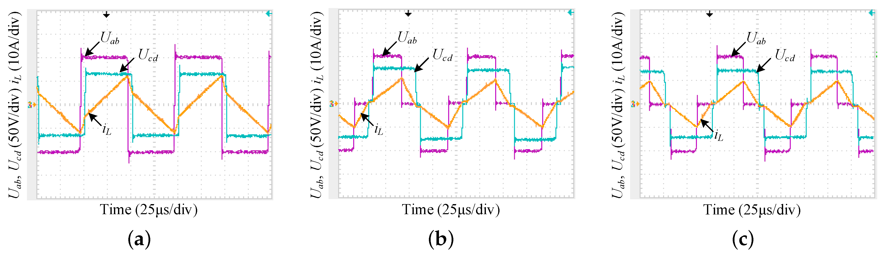
Figure 4 shows the ZVS failure phenomenon under UTPS scheme in some cases. Figure 4a,b shows the ideal waveforms and actual waveforms, respectively. It can be seen that, compared with the ideal waveforms, the instantaneous value of i L is negative at the moment S 3 turns on. It indicates that part of the switches of primary side will operate in hard-switching (HS) state. That is to say, phase-shift errors invalidate the soft-switching operation proposed in UTPS scheme.
(c) Optimal scheme failure: Similar to the soft-switching failure analysis, due to the regulated phase shifts in closed-loop system, the optimization algorithm for the performance indexes, such as current stress, backflow power, etc., will be invalid. 
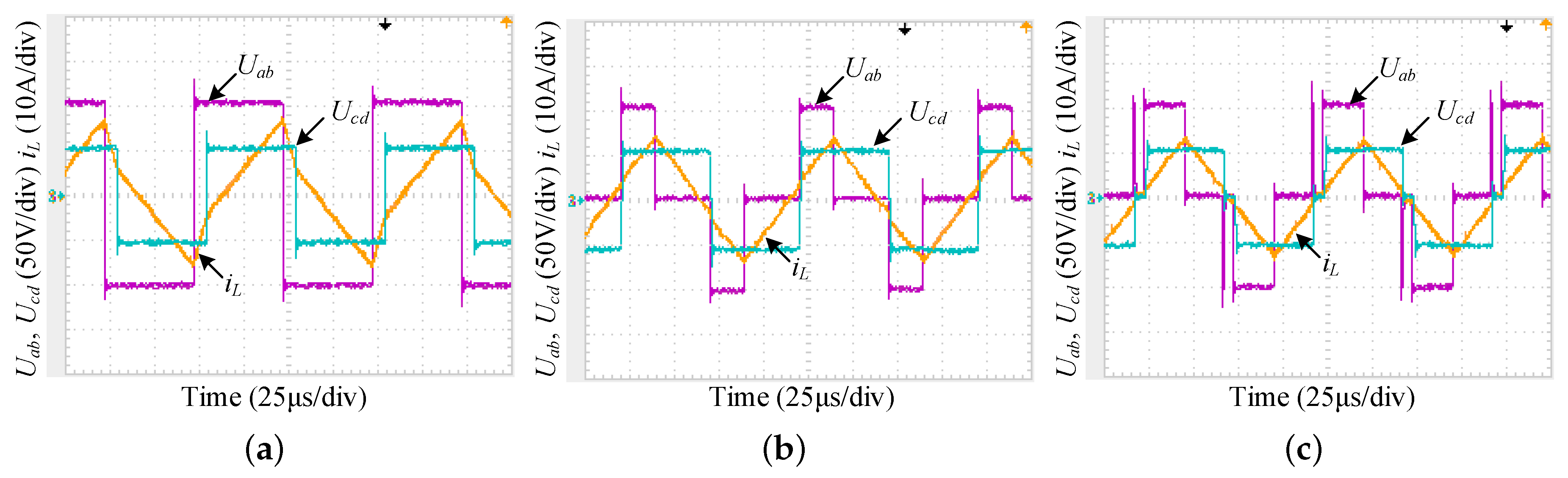
Figure 5a gives the actual waveforms of DAB converter in UTPS scheme, in which the transmission power is 125 W, and the dead-time ratio is 0.1. It can be seen that the actual current stress is 8.8 A under the phase shifts ( D 1 = 0.68 and D 3 = 0.37 ) calculated by UTPS scheme. However, with the same required transmission power and dead time, the current stress can be reduced to 7.55 A with D 1 = 0.58 and D 3 = 0.37 , as shown in Figure 5b. It indicates that the current stress cannot be minimized under the UTPS scheme when taking account of dead time, and the optimal solutions calculated by the ideal power model are not applicable in practical operation.
Due to the problems caused by phase-shift errors, the effectiveness of the traditional optimal schemes cannot be guaranteed in practical applications. As a result, the switching losses and conducting losses will increase, which degrades the performance of DAB converter significantly. From the previous analysis, it can be seen that the fundamental cause of phase-shift errors is the inaccurate power model. Thus, the following section will build an accurate transmission power model incorporating dead time to overcome the drawbacks of phase-shift errors.

3. Operating Mode Analysis and Power Model Derivation Under TPS Control

3.1. Basic Principle of Operating Mode Compartmentalization

In traditional phase-shift control schemes, the waveforms of U ab and U cd are merely affected by the turn-on signal sequence of the eight switches, which is determined by the magnitude and direction of the phase shifts. However, when considering the existence of dead time, besides the turn-on signal sequence, the waveforms are also relevant to the polarity of i L and the value of the dead-time ratio [18,21] . Therefore, the operating modes need to be compartmentalized based on the relationships among the phase-shift ratios, the dead-time ratio and the zero-crossing point.
Assuming that the voltage conversion ratio k = U 1 / n U 2 and k > 1 , the other condition k < 1 can be analyzed similarly. Six operating modes are summarized in traditional TPS scheme as follows [12]:
{ M I : 0 D 1 D 2 D 2 + D 3 1 M II : 0 D 2 D 1 D 2 + D 3 1 M III : 0 D 2 D 2 + D 3 D 1 1 M IV : 0 D 2 + D 3 1 D 2 D 1 1 D 2 + D 3 M V : 0 D 2 + D 3 1 D 1 D 2 1 D 2 + D 3 M VI : 0 D 1 D 2 + D 3 1 D 2 1 D 2 + D 3
These six modes are the ideal operating modes taking no account of dead time, which are merely determined by the relationship among the three phase-shift ratios, and they are defined as main modes in this paper. Subsequently, under each main mode, the dead-time ratio M and zero-crossing-point ratio T 0 need to be sorted together with the three phase-shift ratios. In this way, each main mode can be divided into several sub modes, which are the actual operating modes. Compared with the main modes shown in Equation (2), the number of the sub modes will multiply due to the extra factors M and T 0 . Therefore, it brings challenges to enumerate the sub modes under all main modes. Actually, the studies in [11,13] validate that the sum of the transmission power ranges of M I , M II and M III are wide enough to cover the full operating range, and the traditional optimization algorithms are locked at these three modes (at high power level, the optimization algorithms are locked at M I , and at low power level, the optimization algorithms are locked at the boundary of M II and M III ). Therefore, it is unnecessary to enumerate all sub modes, and the operating mode compartmentalization can be based on M I , M II and M III . In this way, the compartmentalizing procedure will be simplified and the number of the sub modes will be reduced significantly.

3.2. Sub Modes Compartmentalization of DAB Converter

ZVS operation will be guaranteed by ensuring that the active switch turns on when the voltage across the switch is clamped to zero by the conducting antiparallel diode. The ZVS constraints are expressed as follows: ZVS of S 1 , S 4 , Q 3 and Q 2 requires i L < 0 , and that of S 2 , S 3 , Q 1 and Q 4 requires i L > 0 [11,16]. With the ZVS constraints, the zero-crossing-point ratio T 0 can be confined to a certain range when compartmentalizing the sub modes.
In the sub modes of M I , the ZVS constraints can be concluded as
{ i L [ ( D 1 + M ) T h s ] > 0 i L [ ( D 2 + M ) T h s ] < 0
In the sub modes of M III , the ZVS constraints can be concluded as
{ i L ( D 2 T h s ) < 0 i L [ ( D 2 + D 3 + M ) T h s ] < 0 i L ( D 1 T h s ) > 0 i L [ ( D 1 + M ) T h s ] > 0
In M II , some of the power devices cannot achieve ZVS operating, however, it is still worth considering the sub modes under M II due to the good steady-state performance. Firstly, current stress can be minimized in M II during low power range [11,13]. Secondly, when the zero-crossing-point ratio T 0 is restricted to 0 < T 0 < D 2 + M , half of the power devices (S 1 , S 2 , Q 3 and Q 4 ) can turn on at ZVS, and others (S 3 , S 4 , Q 1 and Q 2 ) can turn off at ZCS, therefore the sub modes of M II still have good soft-switching characteristics [11].
M I can be divided into three sub modes, as shown in Figure 6. Due to the symmetry, this paper just takes half a period to analyze the switching characterization under TPS control.
(a) M I 1 : The operation waveforms are shown in Figure 6a, and the operational-mode constraints are
{ 0 D 1 D 2 D 2 + D 3 1 D 1 + M T 0 D 2 + M 0 T 0 D 2
Before the initial time, the current i L is in positive direction, which flows through S 1 and S 4 in the primary side, and M 1 and M 4 in the secondary side, and the converter operates in State 1, as shown in Figure 7a. When S 1 turns off, S 2 will not turn on immediately due to the existence of dead time. In the primary side, the current i L flows through D 2 and S 4 , as shown in Figure 7b. At t = D 1 T hs , S 4 turns off, and the current is carried from D 2 and D 3 to U 1 in the primary side, as shown in Figure 7c. Due to the ZVS constraint D 1 + M T 0 , the turn-on signal of S 3 occurs before t 0 . When i L decreases to zero at t 0 , S 2 and S 3 turn on at ZVS in the primary side, and Q 1 and Q 4 turn on at ZVS in the secondary side. The converter operates in State 4, as shown in Figure 7d. At t = D 2 T hs , Q 1 turns off, the current i L flows through M 2 and Q 4 , as shown in Figure 7e. At t = ( D 2 + D 3 ) T hs , Q 4 turns off, the current i L is carried from M 2 and M 3 to U 2 in the secondary side, as shown in Figure 7f. Note that the turn-on signals of S 2 and Q 2 have no effect on the waveforms as long as the mode-operational constraints are satisfied.
According to the symmetry of the waveforms, the zero-crossing-point ratio T 0 can be derived as
T 0 = k D 1 + 2 D 2 + D 3 + k 1 2 ( k + 1 )
(b) M I 2 : The operation waveforms are shown in Figure 6b, and the operational-mode constraints are
{ 0 D 1 D 2 D 2 + D 3 1 D 1 + M T 0 D 2 + M D 2 T 0 D 2 + D 3
Compared with M I 1 , the conducting devices of M I 2 have differences between D 1 T hs and t 0 T hs . When Q 1 turns off at t = D 2 T hs , the current still flows through M 1 and M 4 due to the unchanged current direction. Therefore, U cd will not turn to zero at t = D 2 T hs until the current decreases to zero.
Similarly, the zero-crossing-point ratio T 0 can be derived as
T 0 = k D 1 + D 2 + D 3 + k 1 2 k + 1
(C) M I 3 : The operation waveforms are shown in Figure 6c, and the operational-mode constraints are
{ 0 D 1 D 2 D 2 + D 3 1 D 1 + M T 0 D 2 + M D 2 + D 3 T 0 1
The conducting devices of this mode have differences after D 2 T hs compared with M I 2 . Due to the ZVS constraints T 0 D 2 + M , before Q 4 turns off, the turn-on signal of Q 2 will not occur. Thus, U cd will not turn to zero before t 0 . At t 0 , none of the four switches in the secondary side are conductive. The current flows through S 2 and S 3 in the primary side, and M 2 and M 3 in the secondary side. Thus, U cd turns from positive to negative directly, which means that U cd becomes two-level voltage in this mode.
Similarly, the zero-crossing-point ratio T 0 can be derived as
T 0 = k 1 + k D 1 2 k
From the waveforms shown in Figure 6, it can be seen that in M I 1 , dead time has no effect on the operating waveforms, which are identical with the traditional waveforms. However, as for M I 2 and M I 3 , in ideal waveforms, U c d turns from 1 to 0 at t = D 2 T h s ; however, in practical waveforms, it occurs at t = T 0 T h s . Therefore, the duty cycle of U cd will be abnormal due to the existence of dead time, and the transmission power model of M I 2 and M I 3 will be different from that in traditional schemes. Once the mode-operational constraints of M I 2 and M I 3 are satisfied, the phase-shift errors will occur in traditional schemes.
With the same analysis, the sub modes under M II and M III can be compartmentalized, as shown in Figure 8 and Figure 9. Note that T 00 , T 01 and T 02 in Figure 9 are three zero-crossing-point ratios of the sub modes of M III . The mode-operational constraints and the expression of T 0 of each sub mode are given in Table 1. As can be seen in Figure 8 and Figure 9, the voltage distortions emerge in various ways in the waveforms. Similarly, the phase-shift errors will occur in traditional schemes when the mode-operational constraints are satisfied.

3.3. Accurate Transmission Power Model Derivation

Based on the analysis of the sub modes, the accurate transmission power model as well as the current stress model can be obtained. For convenience, the transmission power can be normalized as
P 0 = P P N
where P N is defined as
P N = n U 1 U 2 8 f s L r
where f s presents the switching frequency of the power switches. According to Equations (1) and (11), the normalized transmission power of each sub mode can be calculated as
P 0 = { 2 ( D 1 + 2 D 2 + D 3 D 1 2 2 D 2 2 D 3 2 + 2 D 1 D 2 + D 1 D 3 2 D 2 D 3 ) M I 1 2 ( 2 k + 1 ) 2 [ ( 3 k 2 + 3 k + 1 ) D 1 2 + ( 4 k 2 + 4 k + 2 ) ( D 1 D 2 D 3 ) ( D 2 + D 3 ) + ( 2 k 2 + 2 k + 2 ) ( 2 D 2 + 2 D 3 D 1 ) + k 2 + k 2 ] M I 2 1 k 2 ( k 2 1 k 2 D 1 2 ) M I 3 2 ( k 1 ) ( 1 D 1 M ) 2 M II 1 , M II 3 , M II 4 , M II 5 2 [ k D 1 2 ( D 2 + D 3 ) 2 + k M 2 + 2 k D 1 M 2 k D 1 + 2 ( D 2 + D 3 ) 2 k M + k 1 ] M II 2 , M II 6 2 k + 1 [ D 1 2 + 2 ( k 1 ) M 2 + 2 ( k 1 ) D 1 M + 2 ( k + 1 ) D 1 + 4 ( k + 1 ) M + 2 ( k 1 ) ] M II 7 2 k + 1 [ ( k + 1 ) D 1 2 ( k + 2 ) ( D 2 + D 3 ) 2 + k M 2 + 2 ( k + 1 ) D 1 ( D 2 + D 3 ) + 2 k ( D 2 + D 3 ) M 2 ( k + 1 ) D 1 + 4 ( D 2 + D 3 ) 4 k M + 2 ( k 1 ) ] M II 8 2 [ 2 k D 1 + 4 D 2 + 2 D 3 2 M + ( k + 1 ) D 1 2 4 D 1 D 2 2 D 1 D 3 + 2 D 1 M + k 1 ] M III 1 2 ( D 1 + 2 D 2 + D 3 + D 1 2 2 D 1 D 2 D 1 D 3 ) M III 2
The current stress of DAB converter is the peak value of i L . When k > 1 , the peak value occurs at the falling edge of S 1 . Therefore, the current stress can be expressed as i pk = i L ( 0 ) , and, for convenience, it can be normalized as
i 0 = i p k i N
where i N is defined as
i N = P N U 1 = n U 2 8 f s L r
Therefore, the normalized current stress can be derived as
i 0 = { 2 ( k D 1 + 2 D 2 + D 3 + k 1 ) M I 1 2 2 k + 1 [ 2 k 2 D 1 2 + ( 2 k + 2 ) ( D 2 + D 3 ) + 2 k 2 2 ] M I 2 2 k [ k 2 1 ( k 2 k ) D 1 ] M I 3 4 ( k 1 ) ( 1 D 1 M ) M II 1 , M II 3 , M II 4 , M II 5 , M II 7 4 [ ( k 1 ) ( 1 D 2 D 3 ) + k ( D 2 + D 3 D 1 M ) ] M II 2 , M II 6 , M II 8 4 ( k D 1 + 2 D 2 + D 3 M + k 1 ) M III 1 2 ( k D 1 + 2 D 2 + D 3 + k 1 ) M III 2

4. TPSiDT Scheme of DAB Converter

From Equations (13) and (16), it can be seen that the dead-time ratio M affects the transmission power and current stress directly. For guaranteeing the optimality of the proposed algorithm, M is used as another control variable to optimize the system together with the three phase-shift ratios. However, to avoid shoot-through phenomenon, M needs to be larger than a minimum safe value. In this paper, M min is defined as the safe dead-time ratio, which is mainly determined by the turn-on and turn-off times of the power switches. Actually, M min is also the practical value of engineering applications. Therefore, the range of the dead-time ratio is M min M 1.
Naturally, various operating points ( D 1 , D 2 , D 3 , and M) can realize a certain required transmission power. Thus, the minimum-current-stress problem is described as finding the optimal point ( D 1 op , D 2 op , D 3 op , and M op ) that minimize the current stress under the required transmission power and voltage conversion ratio k. The standard form of the optimization problem can be described as
min i 0 ( X ) s . t . P 0 ( X ) P 0 = 0 B i ( X ) 0 , i = 1 , 2 , m
where X = ( D 1 , D 2 , D 3 , M), and P 0 is the required transmission power. B i ( X ) is the assemblage of the mode-operational constraints of each sub mode.
LMM is a general optimization method to obtain the analytic solutions, which can be used for simplifying the design of the control system. The standard form of LMM can be described as
{ E ( X , λ ) = i 0 ( X ) + λ ( P 0 ( X ) P 0 ) E X | X = X = 0 , λ 0
where E ( X , λ ) is the Lagrangian function, λ is the Lagrangian Multiplier, and X = ( D 1 op , D 2 op , D 3 op , M op ) expresses the optimal solution. The Lagrangian function of M I 1 can be expressed as
E ( X , λ ) = 2 k D 1 + 2 D 2 + D 3 + k 1 + λ [ ( D 1 + 2 D 2 + D 3 D 1 2 2 D 2 2 D 3 2 + 2 D 1 D 2 + D 1 D 3 2 D 2 D 3 ) P 0 ]
The equations of LMM in M I 1 can be derived as
{ E D 1 = 2 k + 2 λ ( 1 2 D 1 + 2 D 2 + D 3 ) = 0 E D 2 = 4 + 2 λ ( 2 + 2 D 1 4 D 2 2 D 3 ) = 0 E D 3 = 2 + 2 λ ( 1 + D 1 2 D 2 2 D 3 ) = 0
From Equation (20), D 2 and D 3 can be derived with an expression of D 1 as
{ D 2 = k 2 2 ( k 1 ) D 1 + 1 2 D 3 = 0
According to Equations (13) and (21), the phase-shift ratio D 1 can be expressed with respect to P 0 and k, and the optimization algorithm of M I 1 can be obtained as
{ D 1 = ( k 1 ) 1 P 0 k 2 2 k + 2 D 2 = k 2 2 1 P 0 k 2 2 k + 2 + 1 2 D 3 = 0
To meet the mode-operational constraints of M I 1 , the transmission power range can be deduced as
1 [ k 2 ( k + 1 ) M min ] 2 ( k 2 2 k + 2 ) k 4 P 0 1
In addition, According to Equations (16) and (22), the minimum current stress i 0 min with respect to P 0 and k can be derived as
i 0 min = 2 k 2 ( k 2 2 k + 2 ) ( 1 P 0 )
With the same analysis, the optimal analytic solutions, the power range and the expressions of i 0 min of other modes obtained by LMM can be obtained, as shown in Table 2. It should be noted that, in other sub modes, the expressions of D 1 op , D 2 op , D 3 op and M op with respect to P 0 can hardly be obtained by LMM. For instance, in M II 2 and M II 6 , the equations of LMM are as follows:
{ E D 1 = 4 k + 2 λ ( 2 k D 1 + 2 k M 2 k ) = 0 E D 2 = 4 + 2 λ ( 2 2 D 2 2 D 3 ) = 0 E D 3 = 2 + 2 λ ( 2 2 D 2 2 D 3 ) = 0 E M = 4 k + 2 λ ( 2 k D 1 + 2 k M 2 k ) = 0
It can be seen from Equation (25) that there are merely two effective equations, and the relationship among D 1 , D 2 , D 3 and M can be merely derived as D 1 + M = D 2 + D 3 , thus, the expressions with respect to P 0 of these two modes cannot be obtained by LMM, neither.
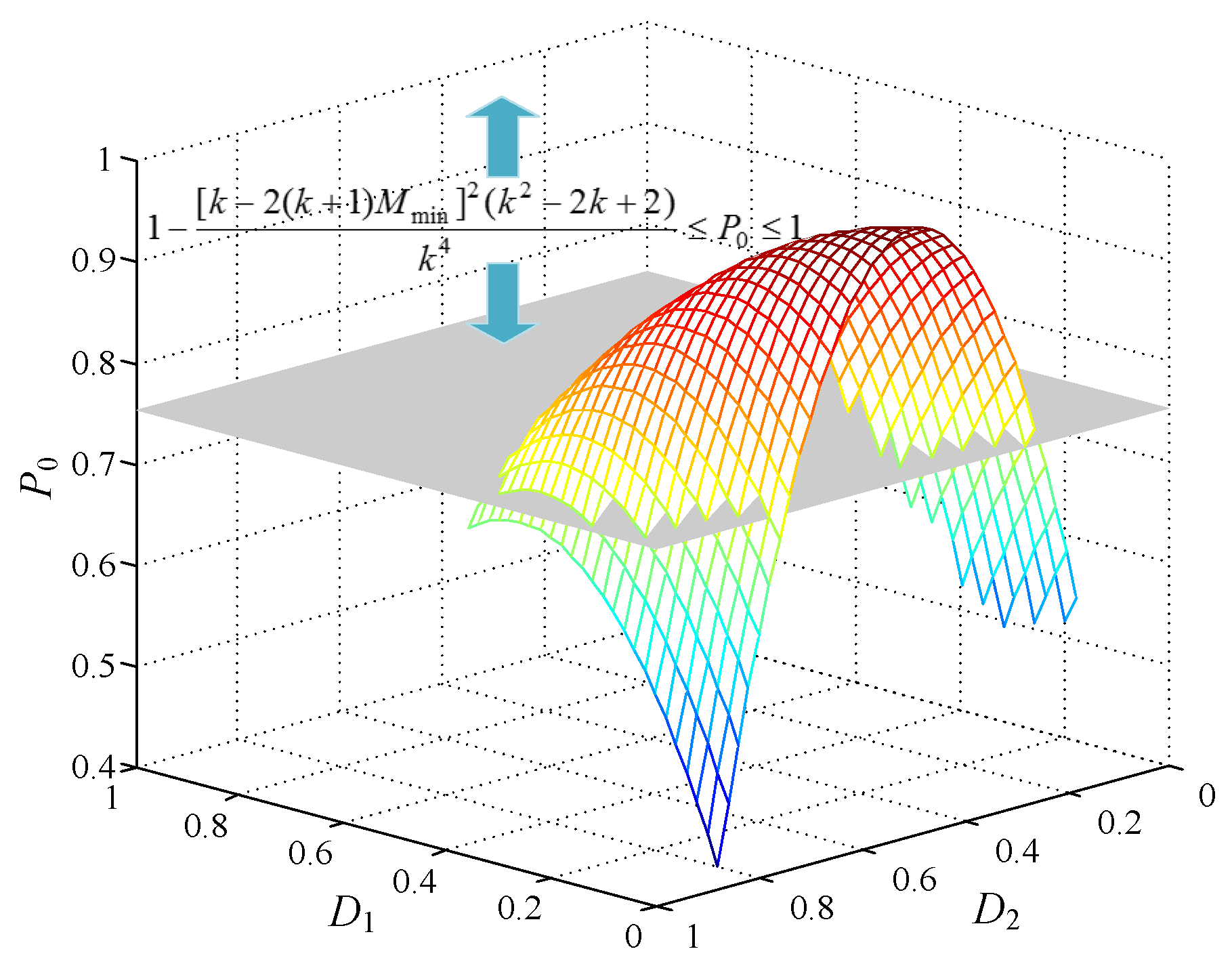
In addition, the power ranges that LMM can be used may be narrower than the whole feasible transmission power range of the sub modes. For instance, Figure 10 gives the feasible power range of M I 1 , in which the gray plane describes the boundary value of Equation (23). By using LMM, the optimal solutions is effective in the power range, as shown in Equation (23). However, from Figure 10, it can be seen that the whole feasible region is wider than Equation (23). Thus, LMM method can only obtain the optimal solutions in partial feasible region. Therefore, by using LMM, the control system can be simplified due to the analytic solutions; however, it cannot guarantee the comprehensiveness of the optimal solutions. In this way, GA is used to compensate the drawbacks of LMM, which can obtain the numerical solutions over the full feasible regions, and the numerical table needs to be generated in practical applications. For guaranteeing the simplicity together with the comprehensiveness of the proposed scheme, the two optimization methods are combined to solve the optimization problem in this paper.
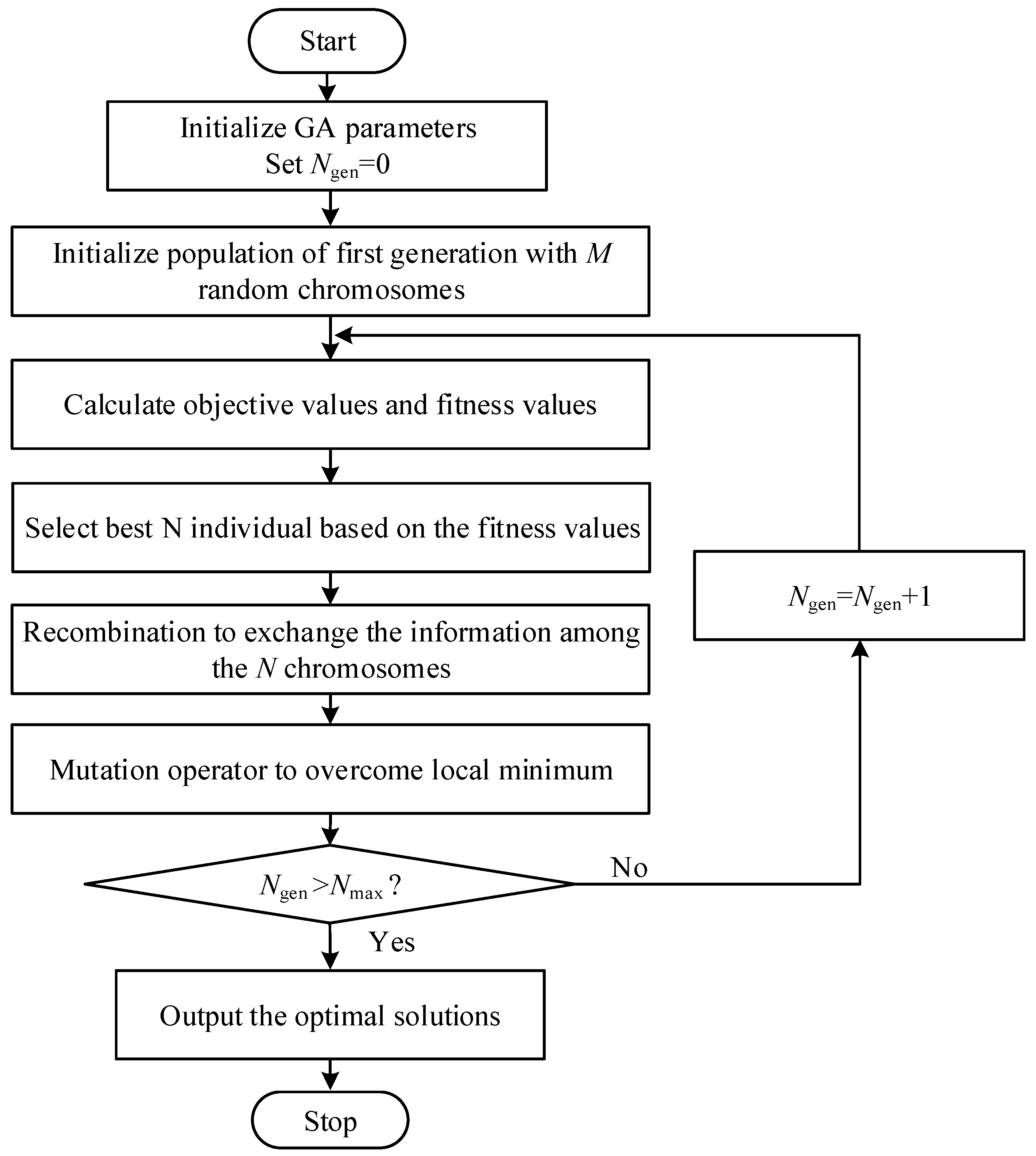
GA is a popular global optimization method due to the advantages of better robustness and parallel characteristics [24]. For the optimization problem, as shown in Equation (17), the GA procedure for acquiring the optimal solutions is shown in Figure 11, in which N gen is the iteration number, and N max is the maximum iteration number. The optimization procedure is operated in the MATLAB R2014a/Optimization Tool, where the current stress model is the fitness function, the reference transmission power and operational-mode constraints are the various constraints. The main parameters of GA such as initial population size and mutation probability are also set in the Optimization Tool.
The relation curves of the minimum current stress i 0 min in each mode with respect to P 0 and k by GA are shown in Figure 12. It should be noted that the feasible power range of M III 1 is too narrow to be considered. In Figure 12, the boundary values of the transmission power obtained by Table 2 are expressed by the dotted lines, which are defined as
{ P A = 1 [ k 2 ( k + 1 ) M min ] 2 ( k 2 2 k + 2 ) k 4 P B = 2 ( k 1 ) ( 1 M min ) 2 k 2
However, the boundary values in M I 3 are not marked in Figure 12. That is because, when k is close to 1, the transmission power range of M I 3 is pretty narrow, and, when k increases, the power range broadens gradually, but the minimum current stress i 0 min is not the least compared with that of other modes. Therefore, M I 3 can be ignored in the optimal scheme. In Figure 12, it can be seen that the power gap between P B and P A becomes wider and wider along with the increase of the safe dead-time ratio M min . When M min approaches to 0, the power gap between P B and P A will disappear, and the optimal scheme will be identical with the traditional ideal scheme. Some information for acquiring the global optimization algorithm can be extracted from Figure 12, which is summarized as follows.
(a) At low power level ( 0 P 0 P B ): In Figure 12, it can be seen that the feasible power range of M III 2 is pretty narrow, especially when M min is relatively large. The values of the minimum current stress of M III 2 are not less than those of the sub modes under M II . In addition, the optimal solutions of M III 2 cannot expressed by analytic solutions, which will bring more inconvenience in practical applications. Therefore, although M III 2 has the ability to make all of the power switches operate at ZVS, it is more meaningful to choose the sub modes under M II during this power range. As can be seen in Table 2, the minimum current stress i 0 min of M II 1 , M II 3 , M II 4 , M II 5 , M II 7 and M II 8 is identical, and the value is less than that of any other mode. Thus, the analytic solutions of M II 1 , M II 3 , M II 4 , M II 5 , M II 7 and M II 8 by LMM are the global optimization algorithm during 0 P 0 P B . Compared with other modes, the voltage distortions will not emerge in M II 5 , which can be seen in the waveforms of 
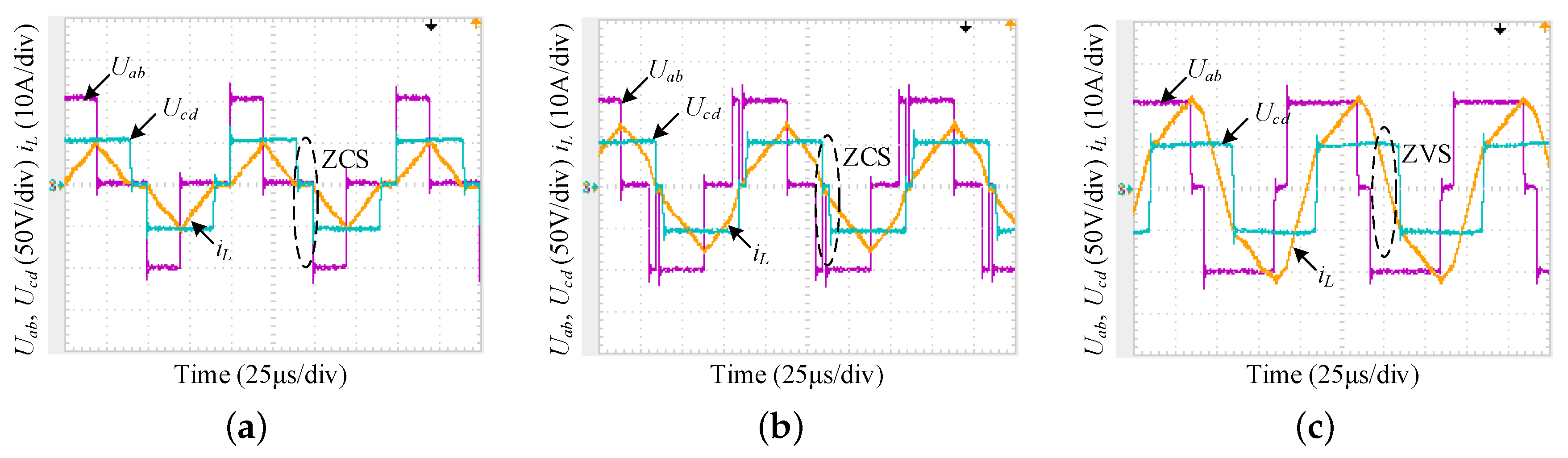
Figure 8e. Therefore, the electromagnetic interference (EMI) and other issues will not be brought by frequent variation of voltage. In addition, as is seen in Table 2, in the optimization algorithm of M II 5 , the dead-time ratio M can be set to M min constantly at low power level, which reduces the complexity of the control system. Therefore, it is meaningful to choose the optimal solutions of M II 5 as the optimization algorithm at low power level. Under the operational-mode constraints of M II 5 , there are various choices of the expressions of D 2 op and D 3 op . Assuming that T 0 = D 2 op and D 2 op + D 3 op = M op + D 1 op , the mode-operational constraints can be easily satisfied. Actually, when choosing the expressions of D 2 op and D 3 op that satisfy D 2 op + D 3 op = M op + D 1 op , the converter actually operates at the boundary of M II 5 and M II 6 . Therefore, the optimization algorithm at low power range can be derived as
{ D 1 op = 1 P 0 2 ( k 1 ) M min D 2 op = ( k 1 ) P 0 2 D 3 op = 1 k P 0 2 ( k 1 ) M op = M min
(b) At high power level ( P A P 0 1 ): With the same analysis of low power level, the analytic solutions of M I 1 calculated by LMM are the global optimization algorithm during this power level. From previous analysis, dead time has no effect on the waveforms of M I 1 . Therefore, to simplify the control system, the dead-time ratio M is set to M min during this power range, and the optimization algorithm in Equation (22) can be rewritten as
{ D 1 op = ( k 1 ) 1 P 0 k 2 2 k + 2 ) D 2 op = k 2 2 1 P 0 k 2 2 k + 2 + 1 2 D 3 op = 0 M op = M min
(c) At middle power level ( P B P 0 P A ): The global optimization algorithm is acquired by GA during this power level. For the required transmission power and voltage conversion ratio, the minimum current stress i 0 of each mode can be obtained. Comparing all the i 0 of each mode, the least value is the optimal current stress, and the control variables realizing the optimal value are the optimal solutions under the required P 0 and k. The optimization algorithm at middle power level cannot be expressed in analytic solutions, therefore, the optimal phase-shift ratios and dead-time ratio require the off-line calculation. Then, the calculated results can be stored in a form of memory of microcontroller, which can be applicable in practical application.
Overall, the optimization algorithm can be expressed in Table 3. As shown in Table 3, at low and high power levels, the dead-time ratio M can be set to M min constantly, and, at middle power level, M can be adaptive in the optimization algorithm.
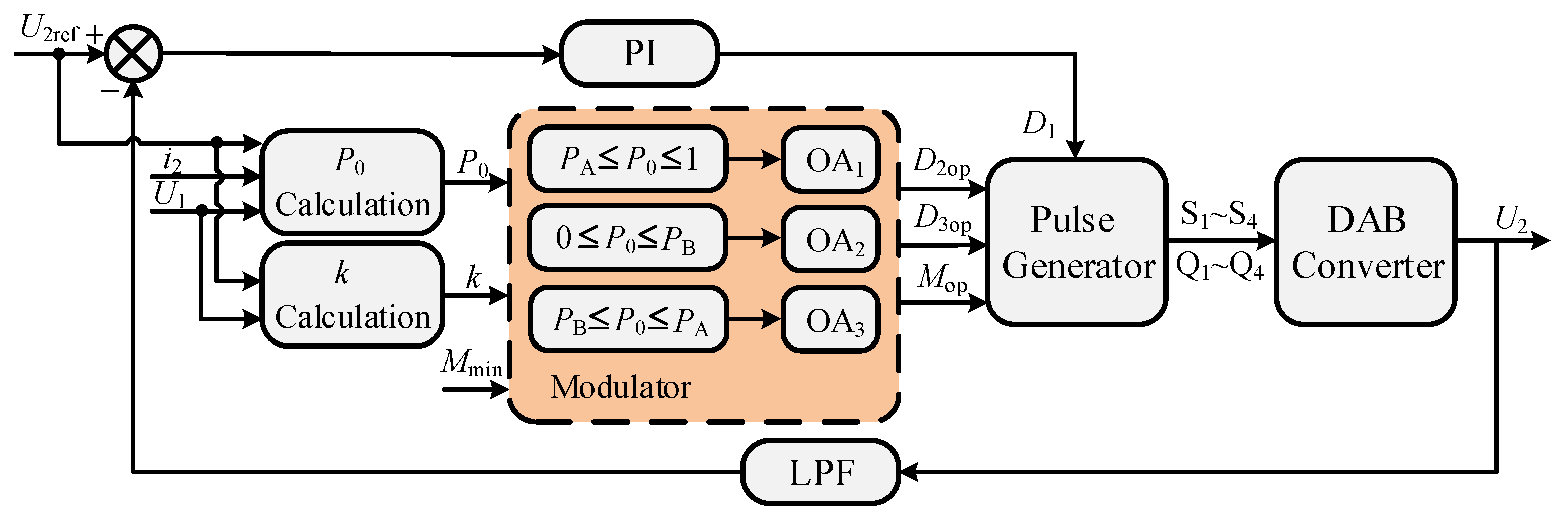
The control diagram of the proposed TPSiDT scheme is shown in Figure 13, in which OA 1 , OA 2 and OA 3 are defined as the optimization algorithm at high power level, low power level, and middle power level, respectively, and U 2 ref is the reference output voltage. In the control diagram, the control system detects the input voltage U 1 , output voltage U 2 , and output current i 2 , and then, the real-time values of the normalized transmission power P 0 and the voltage conversion ratio k can be calculated. To avoid that the voltage conversion ratio k goes to infinity at the start-up stage, U 2 ref is adopted to replace U 2 in k calculation. The safe dead-time ratio M min can be decided by the characteristics of the power devices. Thus, the power boundary values P A and P B can be obtained by Equation (26). Based on the relationships among P 0 , P A and P B , the power level as well as the optimal solutions can be decided. Thereinto, D 2 op , D 3 op , and M op can be determined by the optimization algorithm shown in Table 3, while D 1 is regulated by PI controller to realize the required output voltage and transmission power.

5. Experimental Results

To verify the theoretical analysis mentioned before, a laboratory prototype was constructed based on the TMS320F28335 digital signal processor, and the main parameters are shown in Table 4. In the platform, the safe dead time is 2 μ s, therefore, the dead-time ratio M min is 0.04. However, in many high-switching-frequency DAB converters, the dead-time ratio may reach to 0.2. For instance, in [25], the power devices of primary side are FDMC2610. The switching frequency f s is 1 MHz and the typical dead time is about 100 ns, thus the dead-time ratio M min is 0.2. In [26], the power devices of high-voltage side are IPP65R380FD. The switching frequency f s reaches to 500 kHz, and the dead time of this device is 150∼200 ns, thus the dead-time ratio M min is about 0.15∼0.2. To guarantee the practicability and reasonably evaluate the effectiveness of the proposed scheme in high-switching-frequency converters, the dead-time ratio is varied from 0.04 to 0.24 in [20]. In this study, M min was set to 0.04, 0.1, and 0.15, respectively.

5.1. Power Model Accuracy Experiments

Figure 14 demonstrates the comparative curves of U 2 versus the required transmission power P between the power models of TPSiDT scheme and UTPS scheme. In the experiments, the input voltage U 1 was fixed at 100 V. Under a certain voltage conversion ratio k, the output voltage U 2 was fixed with variable transmission power. For instance, when k = 1 . 5 , the required output voltage U 2 was 66.67 V, which is described by the dotted line. In Figure 14, it can be seen that, in UTPS power model, as the safe dead-time ratio M min increased, the errors between the actual output voltage and the required output voltage increased significantly. Furthermore, the errors became apparent when the converter operated at low loads. However, in TPSiDT power model, the errors were acceptable with various M min and over the full operating range. Therefore, the accuracy of the proposed power model can be explicitly confirmed.

5.2. Optimal Modulation Scheme Experiments

5.2.1. Minimum-Current-Stress Analysis

Figure 15 and Figure 16 illustrate the experimental waveforms of DAB converter under SPS scheme, UTPS scheme and TPSiDT scheme with M min = 0.04 , U 1 = 100 V and P = 300 W. In Figure 15, the voltage conversion ratio k = 1.5 , and it can be seen that the current stress decreased from 11.2 A with SPS scheme, to 10.2 A with UTPS scheme, and to 9.8 A with TPSiDT scheme. On the other hand, in Figure 16, k = 2 , and the current stress decreased from 17.6 A with SPS scheme, to 12 A with UTPS scheme, and to 11.7 A with TPSiDT scheme.
Figure 17 and Figure 18 illustrate the experimental waveforms under SPS scheme, UTPS scheme and TPSiDT scheme with M min = 0.1 , U 1 = 100 V and P = 300 W. In Figure 17, k = 1.5 , and the current stress decreased from 11.7 A with SPS scheme, to 10.8 A with UTPS scheme, and to 9.8 A with TPSiDT scheme. In Figure 18, k = 2 , and the current stress decreased from 15.8 A with SPS scheme, to 13.2 A with UTPS scheme, and to 12.1 A with TPSiDT scheme.
Similarly, Figure 19 and Figure 20 illustrate the experimental waveforms under SPS scheme, UTPS scheme and TPSiDT scheme with M min = 0.15 , U 1 = 100 V and P = 400 W. In Figure 19, k = 1.5 , and it can be seen that the current stress decreased from 12.8 A with SPS scheme, to 12 A with UTPS scheme, and to 11.5 A with TPSiDT scheme. In Figure 20, k = 2 , and the current stress decreased from 17.1 A with SPS scheme, to 15.5 A with UTPS scheme, and to 14.6 A with TPSiDT scheme.

5.2.2. Soft-Switching-Operation Analysis

In Figure 15, Figure 16, Figure 17, Figure 18, Figure 19 and Figure 20, it can also be seen that, in the SPS scheme and UTPS scheme, part of the active switches suffered from HS operation during some power range, which indicates that the soft-switching operation failure occurred in traditional schemes. Figure 21 illustrates the experimental waveforms of DAB with TPSiDT scheme with k = 2 and M min = 0.1 , and the boundary values of the power range could be calculated as P B = 0.405 and P A = 0.755 . The waveforms of low power range, middle power range, and high power range are shown in Figure 21a–c, respectively. It can be seen that the soft-switching constraints of DAB converter could be guaranteed over the full power range; therefore, the converter can operate in soft-switching state in practical applications.

5.2.3. Efficiency and Start-Up Analysis

The current stress and efficiency curves with different M min are shown in Figure 22 and Figure 23, in which the input voltage U 1 is fixed at 100 V, and the voltage conversion ratio is 2. It can be seen that, compared with SPS scheme and UTPS scheme, TPSiDT scheme generated lower current stress and higher efficiency during the whole power range under various M min , especially in light-load condition. Furthermore, with M min increasing, the performance of DAB converter could be improved more significantly, which means that, in the DAB converter that has larger M min , the proposed scheme had better performance on efficiency improvement. Actually, when the safe dead-time ratio M min approached 0, the proposed TPSiDT scheme had the same performance as the traditional optimal TPS scheme, and the range of numerical solutions (middle power level) could be neglected; thus, the control system is not complicated. Therefore, DAB converter would have good performance under various M min by using the proposed scheme.
Figure 24 compares the current stress and efficiency under the three modulation schemes with variable input voltage U 1 . The output voltage was fixed at 50 V and the transmission power was maintained at 300 W. With the increasing of U 1 , the voltage conversion ratio k moved away from unity gradually. It can be seen that, in TPSiDT scheme, the current stress could be reduced under variable k compared with SPS scheme and UTPS scheme. Meanwhile, the efficiency could be improved, especially with high voltage conversion ratio.
The experimental waveforms of the start-up stage under TPSiDT scheme is shown in Figure 25, in which the input voltage is 100 V, the voltage conversion ratio is 2, and the transmission power is 125 W. It can be seen that the optimal modulation scheme could be achieved by the proposed algorithm at steady state.

6. Conclusions

This paper gives a detailed analysis of the phase-shift errors effect caused by dead time, such as output voltage offset, soft-switching failure, optimal scheme failure, etc. To overcome the drawbacks of phase-shift errors, this paper builds an accurate and universal transmission power model incorporating dead time, which serves as a research tool for accurate power prediction and optimal hardware design. Based on the accurate power model and operational-mode constraints, a current stress reduction scheme is proposed based on LMM and GA. Meanwhile, the converter can operate in soft-switching state. In the proposed TPSiDT scheme, the dead-time ratio is regarded as a control variable to guarantee the effectiveness and optimality of the algorithm. Due to the accurate power model, the phase-shift errors will not occur, and the converter can operate in minimum-current stress and soft-switching state in practical applications. Finally, the theoretical analyses were verified by the laboratory prototype, from which the current stress and efficiency of DAB converter were improved in TPSiDT scheme compared with SPS scheme and traditional TPS scheme, especially with high voltage conversion ratio and light load. Furthermore, from the experimental results, it was found that, in a DAB converter that has larger M min , the proposed scheme had better performance on efficiency improvement. The experimental results show the potential advantages of TPSiDT scheme in high-switching-frequency DAB converter by choosing various dead-time ratios; however, they are limited in obtaining the concrete efficiency in high-switching-frequency DAB converter. Actually, if the proposed scheme were applied in high-switching-frequency DAB converter, the performance of the proposed scheme would be better due to more serious dead-time effect. Therefore, the future work is to build a high-switching-frequency experimental platform to verify the proposed scheme more practically, and further analyze the dead-time effect.

Author Contributions

Conceptualization, C.S.; Methodology, C.S.; Software, C.S. and Y.P.; Resources, A.C.; Writing-Review, A.C. and C.D.; Supervision, C.Z. and A.C.

Funding

This work was supported by the National Natural Science Foundation of China (grant numbers 51877128, 61527809) and the Foundation for Innovative Research Groups of National Science Foundation of China (grant number 61821004).

Conflicts of Interest

The authors declare no conflict of interest.

References

  1. Ji, F.F.; Xiang, J.; Li, W.H.; Yue, Q.M. A Feedback Passivation Design for DC Microgrid and Its DC/DC Converters. Energies 2017, 10, 14. [Google Scholar] [CrossRef]
  2. Guo, Z.Q.; Sun, K.; Zhang, L. Analysis and evaluation of dual half-bridge cascaded three-level DC-DC converter for reducing circulating current Loss. IEEE J. Emerg. Sel. Top. Power Electron. 2017, 5, 351–362. [Google Scholar] [CrossRef]
  3. Li, W.H.; Luo, Q.J.; Mei, Y.; Zong, S.; He, X.N.; Xia, C.L. Flying-capacitor-based hybrid LLC converters with input voltage autobalance ability for high voltage applications. IEEE Trans. Power Electron. 2016, 31, 1908–1920. [Google Scholar] [CrossRef]
  4. Li, W.H.; Xu, C.; Luo, H.Z.; Hu, Y.H.; He, X.N.; Xia, C.L. Decoupling-controlled triport composited DC/DC converter for multiple energy interface. IEEE Trans. Ind. Electron. 2015, 62, 4504–4513. [Google Scholar] [CrossRef]
  5. Yu, H.B.; Xiang, X.; Zhao, C.W.; Zhao, Y.; Li, W.H.; He, X.N. Performance analysis of a ZVS bidirectional DC-DC converter with reduced voltage stress on high voltage side. In Proceedings of the 2013 Twenty-Eighth Annual IEEE Applied Power Electronics Conference and Exposition (APEC), Long Beach, CA, 17–21 March 2013; pp. 44–49. [Google Scholar]
  6. Huang, Z.; Sun, K.; Zhang, L. A high light-load efficiency dual active bridge converter with split inductors. In Proceedings of the 2014 IEEE Conference and Expo Transportation Electrification Asia-Pacific (ITEC Asia-Pacific), Beijing, China, 31 August–3 September 2014; pp. 1–5. [Google Scholar]
  7. Shan, Z.Y.; Jatskevich, J.; Iu, H.H.C.; Fernando, T. Simplified load-feedforward control design for dual-active-bridge converters with current-mode modulation. IEEE J. Emerg. Sel. Top. Power Electron. 2018, 6, 2073–2085. [Google Scholar] [CrossRef]
  8. Guo, Z.Q.; Sun, K.; Wu, T.F.; Li, C.B. An Improved modulation scheme of current-fed bidirectional DC-DC converters for loss reduction. IEEE Trans. Power Electron. 2018, 33, 4441–4457. [Google Scholar] [CrossRef]
  9. Wang, L.; Zhu, Q.L.; Yu, W.S.; Huang, A.Q. A medium-voltage medium-frequency isolated DC-DC converter based on 15-kV SiC MOSFETs. IEEE J. Emerg. Sel. Top. Power Electron. 2017, 5, 100–109. [Google Scholar] [CrossRef]
  10. Zong, S.; Luo, H.Z.; Li, W.H.; Deng, Y.; He, X.N. High-power bidirectional resonant DC-DC converter with equivalent switching frequency doubler. IET Renew. Power Gener. 2016, 10, 834–842. [Google Scholar] [CrossRef]
  11. Huang, J.; Wang, Y.; Li, Z.Q.; Lei, W.J. Unified triple-phase-shift control to minimize current stress and achieve full soft-switching of isolated bidirectional DC-DC converter. IEEE Trans. Ind. Electron. 2016, 63, 4169–4179. [Google Scholar] [CrossRef]
  12. Tong, A.P.; Hang, L.J.; Li, G.J.; Jiang, X.C.; Gao, S.Y. Modeling and analysis of dual-active-bridge isolated bidirectional DC/DC converter to minimize RMS current with whole operating range. IEEE Trans. Power Electron. 2018, 33, 5302–5316. [Google Scholar] [CrossRef]
  13. Hou, N.; Song, W.S.; Wu, M.Y. Minimum-current-stress scheme of dual active bridge DC-DC converter with unified-phase-shift control. IEEE Trans. Power Electron. 2016, 31, 8552–8561. [Google Scholar] [CrossRef]
  14. Lu, J.L.; Wang, Y.; Li, X.; Wang, S.D.; Chen, T.J. A boost type control strategy in dual active bridge bidirectional DC-DC converter. In Proceedings of the 2017 IEEE Transportation Electrification Conference and Expo, Asia-Pacific (ITEC Asia-Pacific), Harbin, China, 7–10 August 2017; pp. 1–6. [Google Scholar]
  15. Bai, H.; Mi, C. Eliminate reactive power and increase system efficiency of isolated bidirectional dual-active-bridge DC-DC converters using novel dual-phase-shift control. IEEE Trans. Power Electron. 2008, 23, 2905–2914. [Google Scholar] [CrossRef]
  16. Oggier, G.; García, G.O.; Oliva, A.R. Modulation strategy to operate the dual active bridge dc-dc converter under soft switching in the whole operating range. IEEE Trans. Power Electron. 2011, 26, 1228–1236. [Google Scholar] [CrossRef]
  17. Wu, H.F.; Ding, S.; Sun, K.; Zhang, L.; Li, Y.W.; Xing, Y. Bidirectional soft-switching series-resonant converter with simple PWM control and load-independent voltage-Gain characteristics for energy storage system in DC microgrids. IEEE J. Emerg. Sel. Top. Power Electron. 2017, 5, 995–1007. [Google Scholar] [CrossRef]
  18. Bai, H.; Mi, C.; Gargies, S.Y. The short-time-scale transient processes in high-voltage and high-power isolated bidirectional DC-DC converters. IEEE Trans. Power Electron. 2008, 23, 2648–2656. [Google Scholar] [CrossRef]
  19. Wang, D.Q.; Peng, F.; Ye, J.; Yang, Y.Y.; Emadi, A. Dead-time effect analysis of a three-phase dual-active bridge DC/DC converter. IET Power Electron. 2018, 11, 984–994. [Google Scholar] [CrossRef]
  20. Zhao, B.; Song, Q.; Liu, W.H.; Sun, Y.D. Dead-time effect of the high-frequency isolated bidirectional full-bridge DC-DC converter: Comprehensive theoretical analysis and experimental verification. IEEE Trans. Power Electron. 2014, 29, 1667–1680. [Google Scholar] [CrossRef]
  21. Song, C.C.; Chen, A.L.; Chen, J.; Du, C.S.; Zhang, C.H. Dead-time effect analysis of dual active bridge DC-DC converter with dual-phase-shift control. In Proceedings of the 2017 Chinese Automation Congress (CAC), Jinan, China, 20–22 October 2017; pp. 6545–6550. [Google Scholar]
  22. Xie, Y.H.; Sun, J.; Freudenberg, J.S. Power flow characterization of a bidirectional galvanically isolated high-power DC/DC converter over a wide operating range. IEEE Trans. Power Electron. 2010, 25, 54–65. [Google Scholar] [CrossRef]
  23. Song, C.C.; Chen, A.L.; Chen, J.; Du, C.S.; Zhang, C.H. Current-stress-optimized strategy of dual active bridge DC-DC converter with dead-time effect in single-phase-shift control. In Proceedings of the IECON 2017-43rd Annual Conference of the IEEE Industrial Electronics Society, Beijing, China, 29 October–1 November 2017; pp. 1013–1018. [Google Scholar]
  24. Yang, C.H.; Lin, Y.D.; Chuang, L.Y.; Chang, H.W. Evaluation of Breast Cancer Susceptibility Using Improved Genetic Algorithms to Generate Genotype SNP Barcodes. IEEE/ACM Trans. Comput. Biol. Bioinform. 2013, 10, 361–371. [Google Scholar] [CrossRef] [PubMed]
  25. Costinett, D.; Maksimovic, D.; Zane, R. Design and Control for High Efficiency in High Step-Down Dual Active Bridge Converters Operating at High Switching Frequency. IEEE Trans. Power Electron. 2013, 28, 3931–3940. [Google Scholar] [CrossRef]
  26. He, X.F.; Zhang, Z.L.; Cai, Y.Y.; Liu, Y.F. A variable switching frequency hybrid control for ZVS dual active bridge converters to achieve high efficiency in wide load range. In Proceedings of the 2014 IEEE Applied Power Electronics Conference and Exposition—APEC 2014, Fort Worth, TX, USA, 16–20 March 2014; pp. 1095–1099. [Google Scholar]
Figure 1. Topology of dual active bridge (DAB) converter.
Energies 12 00973 g001
Figure 2. Typical waveforms of DAB converter: (a) ideal triple-phase-shift (TPS) control; and (b) actual TPS control with dead time.
Energies 12 00973 g002
Figure 3. Transient waveforms of DAB converter switching from ideal TPS control to actual TPS control with U 1 = 100 V, P = 125 W, n = 1 , D 1 = 0.68 , D 2 = 0.316 , and D 3 = 0.37 : (a) transient waveform of output voltage; and (b) transient waveform of inductor current.
Energies 12 00973 g003
Figure 4. Simulation waveforms of DAB converter under UTPS scheme with U 1 = 100 V, U 2 = 50 V, and P = 344 W: (a) D 1 = 0.55 , D 3 = 0 , and M = 0 ; and (b) D 1 = 0.55 , D 3 = 0 , and M = 0.1 .
Energies 12 00973 g004
Figure 5. Simulation waveforms of DAB converter with U 1 = 100 V, U 2 = 50 V, and P = 125 W: (a) D 1 = 0.68 , D 3 = 0.37 , and M = 0 ; and (b) D 1 = 0.58 , D 3 = 0.37 , and M = 0.1 .
Energies 12 00973 g005
Figure 6. Waveforms of sub modes under M I : (a) M I 1 ; (b) M I 2 ; and (c) M I 3 .
Energies 12 00973 g006
Figure 7. Operating states under M I : (a) State 1; (b) State 2; (c) State 3; (d) State 4; (e) State 5; and (f) State 6.
Energies 12 00973 g007
Figure 8. Waveforms of sub modes under M II : (a) M II 1 ; (b) M II 2 ; (c) M II 3 ; (d) M II 4 ; (e) M II 5 ; (f) M II 6 ; (g) M II 7 ; and (h) M II 8 .
Energies 12 00973 g008
Figure 9. Waveforms of sub modes under M III : (a) M III 1 ; and (b) M III 2 .
Energies 12 00973 g009
Figure 10. Feasible region of M I 1 with k = 1.5 , M = 0.1 , D 3 = 0 .
Energies 12 00973 g010
Figure 11. Flow chart of genetic algorithm (GA).
Energies 12 00973 g011
Figure 12. Curves of the minimum current stress in each sub modes: (a) M min = 0.02 ; (b) M min = 0.05 ; and (c) M min = 0.1 .
Energies 12 00973 g012
Figure 13. Control diagram of TPSiDT scheme.
Energies 12 00973 g013
Figure 14. Comparative curves of the output voltage: (a) k = 1.5 ; and (b) k = 2 .
Energies 12 00973 g014
Figure 15. Experimental waveforms of DAB converter with M min = 0.04 , k = 1.5 , U 1 = 100 V, P = 300 W: (a) single-phase-shift (SPS) scheme; (b) unified triple-phase-shift (UTPS) scheme; and (c) TPSiDT scheme.
Energies 12 00973 g015
Figure 16. Experimental waveforms of DAB converter with M min = 0.04 , k = 2 , U 1 = 100 V, P = 300 W: (a) SPS scheme; (b) UTPS scheme; and (c) TPSiDT scheme.
Energies 12 00973 g016
Figure 17. Experimental waveforms of DAB converter with M min = 0.1 , k = 1.5 , U 1 = 100 V, P = 300 W: (a) SPS scheme; (b) UTPS scheme; and (c) TPSiDT scheme.
Energies 12 00973 g017
Figure 18. Experimental waveforms of DAB converter with M min = 0.1 , k = 2 , U 1 = 100 V, P = 300 W: (a) SPS scheme; (b) UTPS scheme; and (c) TPSiDT scheme.
Energies 12 00973 g018
Figure 19. Experimental waveforms of DAB converter with M min = 0.15 , k = 1.5 , U 1 = 100 V, P = 400 W: (a) SPS scheme; (b) UTPS scheme; and (c) TPSiDT scheme.
Energies 12 00973 g019
Figure 20. Experimental waveforms of DAB converter with M min = 0.15 , k = 2 , U 1 = 100 V, P = 400 W: (a) SPS scheme; (b) UTPS scheme; and (c) TPSiDT scheme.
Energies 12 00973 g020
Figure 21. Experimental waveforms of DAB converter under TPSiDT scheme with M min = 0.1 , k = 2 , U 1 = 100 V: (a) P = 200 W (low power level); (b) P = 400 W (middle power level); and (c) P = 600 W (high power level).
Energies 12 00973 g021
Figure 22. Current stress curves versus the transmission power P: (a) M min = 0.04 ; and (b) M min = 0.1 ; (c) M min = 0.15 .
Energies 12 00973 g022
Figure 23. Efficiency curves versus the transmission power P: (a) M min = 0.04 ; (b) M min = 0.1 ; and (c) M min = 0.15 .
Energies 12 00973 g023
Figure 24. Experimental curves versus the input voltage U 1 with M min = 0.1 : (a) current stress; and (b) efficiency.
Energies 12 00973 g024
Figure 25. Start-up response of DAB converter under TPSiDT scheme.
Energies 12 00973 g025
Table 1. Operational-Mode Constraints of DAB Converter.
ModeOperational-Mode ConstraintsZero-Crossing-Point Ratio T 0
M I 1 0 D 1 D 2 D 2 + D 3 1
M + D 1 T 0 M + D 2
0 T 0 D 2 k D 1 + 2 D 2 + D 3 + k 1 2 ( k + 1 )
M I 2 D 2 T 0 D 2 + D 3 k D 1 + D 2 + D 3 + k 1 2 k + 1
M I 3 D 2 + D 3 T 0 1 k 1 + k D 1 2 k
M II 1 D 2 M
D 2 + D 3 M + D 1
( k 1 ) ( 1 D 1 M )
M II 2 0 D 2 D 1 D 2 + D 3 1
0 T 0 M + D 2
0 T 0 D 2 D 2 M
D 2 + D 3 M + D 1
( k 1 ) ( 1 D 1 M ) + k ( D 2 + D 3 D 1 M )
M II 3 D 2 M , T 0 M
D 2 + D 3 M + D 1
( k 1 ) ( 1 D 1 M )
M II 4 D 2 M , T 0 M
D 2 + D 3 M + D 1
( k 1 ) ( 1 D 1 M )
M II 5 D 2 T 0 D 1 D 2 + D 3 M + D 1 ( k 1 ) ( 1 D 1 M )
M II 6 D 2 + D 3 M + D 1 ( k 1 ) ( 1 D 1 M ) + k ( D 2 + D 3 D 1 M )
M II 7 D 1 T 0 1 D 2 + D 3 M + D 1 ( k 1 ) ( 1 D 1 M ) + k D 1 k + 1
M II 8 D 2 + D 3 M + D 1 D 2 + D 3 k M + k 1 k + 1
M III 1 0 D 2 D 2 + D 3 D 1 1
0 < T 00 < D 2
D 2 + D 3 + M < T 01 < D 1
D 1 + M < T 02 < 1
T 00 < M T 00 = k D 1 + 2 D 2 + D 3 M + k 1
T 01 = 2 D 2 + D 3 M
T 02 = k D 1 2 D 2 D 3 + M k 1
M III 2 T 00 M T 00 = k D 1 + 2 D 2 + D 3 + k 1 2
T 01 = k D 1 + 2 D 2 + D 3 k + 1 2
T 02 = k D 1 2 D 2 D 3 + k 1 2 ( k 1 )
Table 2. Optimal Solutions of Each Mode Calculated by Lagrange multiplier method (LMM).
ModeRange of P 0 Optimal SolutionsMinimum Current Stress i 0 min
M I 1 1 [ k 2 ( k + 1 ) M min ] 2 ( k 2 2 k + 2 ) k 4 P 0 1 D 1 op = ( k 1 ) 1 P 0 k 2 2 k + 2 ) 2 k 2 ( k 2 2 k + 2 ) ( 1 P 0 )
D 2 op = k 2 2 1 P 0 k 2 2 k + 2 + 1 2
D 3 op = 0
M I 3 k 2 1 ( k 1 2 k M min ) 2 k 2 P 0 k 2 1 k 2 D 1 op = k 2 1 k 2 P 0 k 2 ( k 1 ) ( k + 1 k 2 1 k 2 P 0 ) k
M II 1 , M II 3 ,
M II 4 , M II 5
0 P 0 2 ( k 1 ) ( 1 M min ) 2 k 2 D 1 op + M op = 1 P 0 2 ( k 1 ) 2 2 ( k 1 ) P 0
M II 7 0 P 0 2 ( k 1 ) ( 1 M min ) 2 k 2 D 1 op = ( k 1 ) P 0 2 2 2 ( k 1 ) P 0
M op = 1 k P 0 2 ( k 1 )
M II 8 0 P 0 2 ( k 1 ) ( 1 M min ) 2 k 2 D 1 op = ( k 1 ) P 0 2 2 2 ( k 1 ) P 0
M op = 1 k P 0 2 ( k 1 )
D 2 op + D 3 op = 1 P 0 2 ( k 1 )
Table 3. Optimization Algorithm of TPS incorporating dead time (TPSiDT) Scheme.
Range of P 0 Optimization Algorithm of the Proposed Scheme
Symbol D 1 op D 2 op D 3 op M op
P A P 0 1 OA 1 ( k 1 ) 1 P 0 k 2 2 k + 2 k 2 2 1 P 0 k 2 2 k + 2 + 1 2 0 M min
0 P 0 P B OA 2 1 P 0 2 ( k 1 ) M min ( k 1 ) P 0 2 1 k P 0 2 ( k 1 ) M min
P B P 0 P A OA 3 Look Up Table
Table 4. Main Parameters of DAB Converter.
ParametersValue
DC input voltage U 1 0∼120 V
DC output voltage U 2 0∼100 V
Input DC capacitor C 1 4000 μ F
Output DC capacitor C 2 4000 μ F
Transformer turns ratio n1
Auxiliary inductor L r 100 μ H
Switching frequency f s 10 kHz
Safe dead-time ratio M min 0.04, 0.1, 0.15

