Evaluation of Interconnection Configuration Schemes for PV Modules with Switched-Inductor Converters under Partial Shading Conditions


Abstract
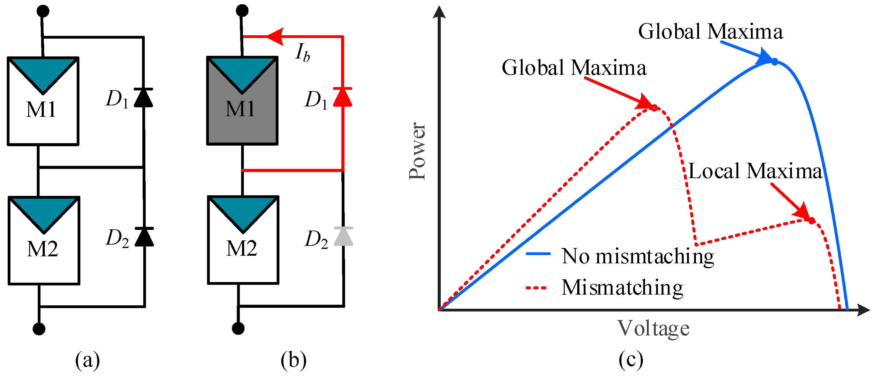
:1. Introduction
2. Configurations and Shading Pattern Designs
2.1. One Module Shading
2.2. Short Wide Shading
2.3. Long Narrow Shading
2.4. Central Shading
2.5. Diagonal Shading
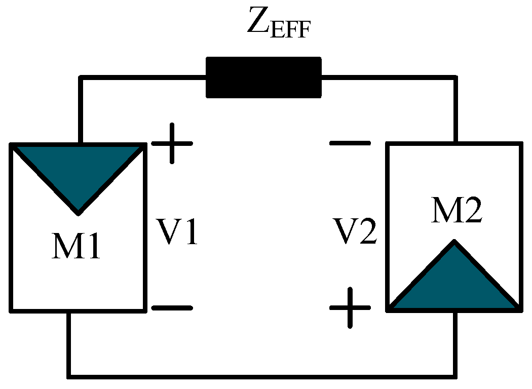
3. Results and Discussion
4. Conclusions
Author Contributions
Funding
Conflicts of Interest
References
- Cancino-Solórzano, Y.; Paredes-Sánchez, J.P.; Gutiérrez-Trashorras, A.J.; Xiberta-Bernat, J. The development of renewable energy resources in the State of Veracruz, Mexico. Utilities Policy 2016, 39, 1–4. [Google Scholar] [CrossRef]
- Fahrenbruch, A.; Bube, R. Fundamentals Of Solar Cells: Photovoltaic Solar Energy Conversion; Elsevier: Amsterdam, The Netherlands, 2012; ISBN 978-0-32-314538-1. [Google Scholar]
- Subudhi, B.; Pradhan, R. A Comparative Study on Maximum Power Point Tracking Techniques for Photovoltaic Power Systems. IEEE Trans. Sustain. Energy 2013, 4, 89–98. [Google Scholar] [CrossRef]
- Sahoo, S.K. Renewable and sustainable energy reviews solar photovoltaic energy progress in India: A review. Renew. Sustain. Energy Rev. 2016, 59, 927–939. [Google Scholar] [CrossRef]
- Ahmed, J.; Salam, Z. A critical evaluation on maximum power point tracking methods for partial shading in PV systems. Renew. Sustain. Energy Rev. 2015, 47, 933–953. [Google Scholar] [CrossRef]
- Niazi, K.A.K.; Yang, Y.; Khan, H.A.; Sera, D. Performance Benchmark of Bypassing Techniques for Photovoltaic Modules. In Proceedings of the 2019 IEEE Applied Power Electronics Conference and Exposition (APEC), Anaheim, CA, USA, 17–21 March 2019. [Google Scholar]
- Pareek, S.; Dahiya, R. Enhanced power generation of partial shaded photovoltaic fields by forecasting the interconnection of modules. Energy 2016, 95, 561–572. [Google Scholar] [CrossRef]
- Niazi, K.; Khan, H.A.; Amir, F. Hot-spot reduction and shade loss minimization in crystalline-silicon solar panels. J. Renew. Sustain. Energy 2018, 10, 1–8. [Google Scholar] [CrossRef]
- Yang, Y.; Kim, K.A.; Blaabjerg, F.; Sangwongwanich, A. Advances in Grid-Connected Photovoltaic Power Conversion Systems; Woodhead Publishing: Cambridge, UK, 2018; ISBN 978-0-08-102342. [Google Scholar]
- Ahsan, S.; Niazi, K.A.K.; Khan, H.A.; Yang, Y. Hotspots and performance evaluation of crystalline-silicon and thin-film photovoltaic modules. Microelectron. Reliab. 2018, 88–90, 1014–1018. [Google Scholar] [CrossRef]
- Ishaque, K.; Salam, Z. A review of maximum power point tracking techniques of PV system for uniform insolation and partial shading condition. Renew. Sustain. Energy Rev. 2013, 19, 475–488. [Google Scholar] [CrossRef]
- Eltawil, M.A.; Zhao, Z. MPPT techniques for photovoltaic applications. Renew. Sustain. Energy Rev. 2013, 25, 793–813. [Google Scholar] [CrossRef]
- Nasir, M.; Zia, M.F. Global maximum power point tracking algorithm for photovoltaic systems under partial shading conditions. In Proceedings of the 16th International Power Electronics and Motion Control Conference and Exposition, Antalya, Turkey, 21–24 September 2014. [Google Scholar]
- Alajmi, B.N.; Ahmed, K.H.; Finney, S.J.; Williams, B.W. A Maximum Power Point Tracking Technique for Partially Shaded Photovoltaic Systems in Microgrids. IEEE Trans. Ind. Electron. 2013, 60, 1596–1606. [Google Scholar] [CrossRef]
- Niazi, K.; Akhtar, W.; Khan, H.A.; Sohaib, S.; Nasir, A.K. Binary Classification of Defective Solar PV Modules Using Thermography. In Proceedings of the 2018 IEEE 7th World Conference on Photovoltaic Energy Conversion (WCPEC), Waikoloa, HI, USA, 10–15 June 2018. [Google Scholar]
- Liu, Y.-H.; Liu, C.-L.; Huang, J.-W.; Chen, J.-H. Neural-network-based maximum power point tracking methods for photovoltaic systems operating under fast changing environments. Sol. Energy 2013, 89, 42–53. [Google Scholar] [CrossRef]
- Daraban, S.; Petreus, D.; Morel, C. A novel MPPT (maximum power point tracking) algorithm based on a modified genetic algorithm specialized on tracking the global maximum power point in photovoltaic systems affected by partial shading. Energy 2014, 74, 374–388. [Google Scholar] [CrossRef]
- Salam, Z.; Ahmed, J.; Merugu, B.S. The application of soft computing methods for MPPT of PV system: A technological and status review. Appl. Energy 2013, 107, 135–148. [Google Scholar] [CrossRef]
- Niazi, K.A.K.; Yang, Y.; Sera, D. Review of mismatch mitigation techniques for PV modules. IET Renew. Power Gener. 2019. [Google Scholar] [CrossRef]
- Kim, K.A.; Shenoy, P.S.; Krein, P.T. Converter Rating Analysis for Photovoltaic Differential Power Processing Systems. IEEE Trans. Power Electron. 2015, 30, 1987–1997. [Google Scholar] [CrossRef]
- Jeon, Y.; Lee, H.; Kim, K.A.; Park, J. Least Power Point Tracking Method for Photovoltaic Differential Power Processing Systems. IEEE Trans. Power Electron. 2017, 32, 1941–1951. [Google Scholar] [CrossRef]
- Khan, O.; Xiao, W. Review and qualitative analysis of submodule-level distributed power electronic solutions in PV power systems. Renew. Sustain. Energy Rev. 2017, 76, 516–528. [Google Scholar] [CrossRef]
- Stauth, J.T.; Seeman, M.D.; Kesarwani, K. Resonant Switched-Capacitor Converters for Sub-module Distributed Photovoltaic Power Management. IEEE Trans. Power Electron. 2013, 28, 1189–1198. [Google Scholar] [CrossRef]
- Tahmasbi-Fard, M.; Tarafdar-Hagh, M.; Pourpayam, S.; Haghrah, A. A Voltage Equalizer Circuit to Reduce Partial Shading Effect in Photovoltaic String. IEEE J. Photovolt. 2018, 8, 1102–1109. [Google Scholar] [CrossRef]
- Jeong, H.; Lee, H.; Liu, Y.; Kim, K.A. Review of Differential Power Processing Converter Techniques for Photovoltaic Applications. IEEE Trans. Energy Convers. 2019, 34, 351–360. [Google Scholar] [CrossRef]
- Karatepe, E.; Boztepe, M.; Çolak, M. Development of a suitable model for characterizing photovoltaic arrays with shaded solar cells. Sol. Energy 2007, 81, 977–992. [Google Scholar] [CrossRef]
- La Manna, D.; Li Vigni, V.; Riva Sanseverino, E.; Di Dio, V.; Romano, P. Reconfigurable electrical interconnection strategies for photovoltaic arrays: A review. Renew. Sustain. Energy Rev. 2014, 33, 412–426. [Google Scholar] [CrossRef]
- Satpathy, P.R.; Jena, S.; Sharma, R. Power enhancement from partially shaded modules of solar PV arrays through various interconnections among modules. Energy 2018, 144, 839–850. [Google Scholar] [CrossRef]
- Kadri, R.; Andrei, H.; Gaubert, J.-P.; Ivanovici, T.; Champenois, G.; Andrei, P. Modeling of the photovoltaic cell circuit parameters for optimum connection model and real-time emulator with partial shadow conditions. Energy 2012, 42, 57–67. [Google Scholar] [CrossRef]
- Satpathy, P.R.; Jena, S.; Jena, B.; Sharma, R. Comparative study of interconnection schemes of modules in solar PV array network. In Proceedings of the 2017 International Conference on Circuit, Power and Computing Technologies (ICCPCT), Kollam, India, 20–21 April 2017. [Google Scholar]
- Velasco-Quesada, G.; Guinjoan-Gispert, F.; Pique-Lopez, R.; Roman-Lumbreras, M.; Conesa-Roca, A. Electrical PV Array Reconfiguration Strategy for Energy Extraction Improvement in Grid-Connected PV Systems. IEEE Trans. Ind. Electron. 2009, 56, 4319–4331. [Google Scholar] [CrossRef]
- Lavado Villa, L.F.; Ho, T.-P.; Crebier, J.-C.; Raison, B. A Power Electronics Equalizer Application for Partially Shaded Photovoltaic Modules. IEEE Trans. Ind. Electron. 2013, 60, 1179–1190. [Google Scholar] [CrossRef]
- Satpathy, P.R.; Sharma, R.; Jena, S. A shade dispersion interconnection scheme for partially shaded modules in a solar PV array network. Energy 2017, 139, 350–365. [Google Scholar] [CrossRef]
- Malathy, S.; Ramaprabha, R. Reconfiguration strategies to extract maximum power from photovoltaic array under partially shaded conditions. Renew. Sustain. Energy Rev. 2018, 81, 2922–2934. [Google Scholar] [CrossRef]
- Rana, A.S.; Nasir, M.; Khan, H.A. String level optimisation on grid-tied solar PV systems to reduce partial shading loss. IET Renew. Power Gener. 2017, 12, 143–148. [Google Scholar] [CrossRef]


| Parameters | Rating |
|---|---|
| Rated Peak Power (Pmax) | 60 W |
| Voltage at MPP (Vmp) | 17.10 V |
| Current at MPP (Imp) | 3.50 A |
| Open Circuit Voltage (Voc) | 21.10 V |
| Short Circuit Current (Isc) | 3.80 A |
© 2019 by the authors. Licensee MDPI, Basel, Switzerland. This article is an open access article distributed under the terms and conditions of the Creative Commons Attribution (CC BY) license (http://creativecommons.org/licenses/by/4.0/).
Share and Cite
Niazi, K.A.K.; Yang, Y.; Nasir, M.; Sera, D. Evaluation of Interconnection Configuration Schemes for PV Modules with Switched-Inductor Converters under Partial Shading Conditions. Energies 2019, 12, 2802. https://doi.org/10.3390/en12142802
Niazi KAK, Yang Y, Nasir M, Sera D. Evaluation of Interconnection Configuration Schemes for PV Modules with Switched-Inductor Converters under Partial Shading Conditions. Energies. 2019; 12(14):2802. https://doi.org/10.3390/en12142802
Chicago/Turabian StyleNiazi, Kamran Ali Khan, Yongheng Yang, Mashood Nasir, and Dezso Sera. 2019. "Evaluation of Interconnection Configuration Schemes for PV Modules with Switched-Inductor Converters under Partial Shading Conditions" Energies 12, no. 14: 2802. https://doi.org/10.3390/en12142802
APA StyleNiazi, K. A. K., Yang, Y., Nasir, M., & Sera, D. (2019). Evaluation of Interconnection Configuration Schemes for PV Modules with Switched-Inductor Converters under Partial Shading Conditions. Energies, 12(14), 2802. https://doi.org/10.3390/en12142802