Article

Experimental Comparison of Two-Level Full-SiC and Three-Level Si–SiC Quasi-Z-Source Inverters for PV Applications

by
Serhii Stepenko
1,2,*,
Oleksandr Husev
1,3,
Dmitri Vinnikov
1,
Carlos Roncero-Clemente
4,
Sergio Pires Pimentel
1,5 and
Elena Santasheva
1,4
1
Department of Electrical Power Engineering and Mechatronics, Tallinn University of Technology, 19086 Tallinn, Estonia
2
Department of Information Measuring Technologies, Metrology and Physics, Chernihiv National University of Technology, 14027 Chernihiv, Ukraine
3
Biomedical Radioelectronic Apparatus and Systems Department, Chernihiv National University of Technology, 14027 Chernihiv, Ukraine
4
Department of Electrical, Electronic and Control Engineering, School of Industrial Engineering, University of Extremadura, 06006 Badajoz, Spain
5
School of Electrical, Mechanical, and Computer Engineering, Federal University of Goias (UFG), Goiania 74690-900, Brazil
*
Author to whom correspondence should be addressed.
Energies 2019, 12(13), 2509; https://doi.org/10.3390/en12132509
Submission received: 6 June 2019 / Revised: 24 June 2019 / Accepted: 25 June 2019 / Published: 28 June 2019

Abstract

:
The paper presents a comparative study of two solar string inverters based on the Quasi-Z-Source (QZS) network. The first solution comprises a full-SiC two-level QZS inverter, while the second design was built based on a three-level neutral-point-clamped QZS inverter with Silicon based Metal–Oxide–Semiconductor Field-Effect Transistors (Si MOSFETs). Several criteria were taken into consideration: the size of passive elements, thermal design and size of heatsinks, voltage stress across semiconductors, and efficiency investigation. The Photovoltaic (PV)-string rated at 1.8 kW power was selected as a case study system. The advantages and drawbacks of both solutions are presented along with conclusions.

1. Introduction

Continuous development and improvements of Photovoltaic (PV) system designs along with related technologies, such as Wide Bandgap (WBG) GaN/SiC devices, Digital Signal Processor (DSP)- and Field-Programmable Gate Array (FPGA)-based control units have gradually decreased their costs. This allows new solutions featuring high efficiency and easy implementation which make them commercially attractive. At the same time, power rates and voltage operation ranges determine the availability of certain PV applications, especially in small-scale installations. In addition to efficiency and power density, the reliability of PV inverters is the key factor influencing the feasibility of single-phase industrial implementations [1,2], where Full-Bridge (FB) Voltage-Source Inverters (VSIs) are mostly used. Many DC–AC solutions for connecting PV modules to a single-phase grid are discussed in Reference [3]. The relative costs assessed based on the calculated ratings, component surveys at different vendors, and linear regression analysis were also taken into account in the evaluation.
The Z-Source Inverter (ZSI) [4] is an alternative to VSIs and Current-Source Inverters (CSIs) due to its ability to provide buck–boost operation within the single stage and its improved reliability based on its natural immunity against short-circuit. Its benefits have made it a promising solution for PV systems and have urged investigations in this area, which has resulted in many DC–DC and DC–AC topologies for single-phase and three-phase applications [5,6,7,8,9,10,11,12,13,14,15].
The Quasi-Z-Source Inverter (QZSI) was derived from the ZSI and has become a desirable topology for PV applications [5] due to its inheritance of all the advantages of ZSI enhanced by lower component ratings and continuous input current. The application of multilevel inverters has advantages in higher power designs, where the high voltage stress on the inverter’s switches can be avoided [16,17,18,19]. The combination of the QZSI with the Three-Level (3L) Neutral-Point-Clamped (NPC) inverter has created a new promising topology, described in detail in Reference [6]. It features certain advantages such as low voltage stress on the power switches, single-stage buck–boost operation, continuous input current, short-circuit immunity, and low total harmonic distortion of the output voltage and current.
A detailed comparative study of basic and derived impedance-source networks for buck–boost inverter applications is provided in Reference [7], mostly for three-phase applications. The investigation of loss distribution was addressed recently in References [8,9] for QZSI-based topologies along with methods for their reduction and efficiency improvement.
Many publications devoted to the ZSI- and QZSI-derived solutions for PV, wind, and Microgrids applications have appeared recently [10,11,12,13,14]. They address certain issues, such as current harmonics reduction, voltage gain improvement, leakage current reduction, etc. The authors of Reference [11] emphasize the use of the coupled-inductor and SiC devices to optimize power density. A good comparison of impedance-source networks suitable for DC and AC applications by means of the passive components’ number and size, semiconductor devices stress, and range of the input voltage variation is provided in Reference [15]. The increased voltage stress across semiconductors was reported as the main drawback of ZSI/QZSI. High-voltage gain solutions with additional magnetics may mitigate this.
An extreme high efficiency of 99.4% was reported for a three-phase 50 kW full-SiC PV string inverter in Reference [20]. Another full-SiC solution for a 25 kW three-phase PV string inverter demonstrated 97.7% peak efficiency [21]. These are examples of extra high efficiency, which, however, can be achieved much easier in high-power systems. The latter includes a detailed step-by-step explanation and design guidelines for all the components of the system.
Some low-power low-voltage designs are presented in References [22,23,24,25,26]. An example of an efficient converter based on the zeta inverter topology using 300 V Si + 1200 V SiC Metal–Oxide–Semiconductor Field-Effect Transistors (MOSFETs) is provided in Reference [22], with efficiency up to 95%; however, the nominal power was 220 W and the maximal was 440 W. A CSI-based single-phase solution for leakage current reduction is shown in Reference [23], where Insulated-Gate Bipolar Transistors (IGBTs) were used.
Several 350–400 W designs based on a quasi-switched-boost inverter with an efficiency of 91.3–94% are reported in References [24,25]. A good analysis of power losses, efficiency, and temperature is provided in Reference [26] for a CSI-based solution with SiC MOSFETs; additionally, power losses for all-SiC and hybrid approaches were analyzed, but the experimental results are not shown in the paper.
A valuable and interesting experimental comparison presented in Reference [27] is devoted to three topologies of a three-phase Two-Level (2L) inverter: a QZSI, a VSI with a boost converter, and a VSI with an interleaved boost converter. A detailed description of the methodology for comparison could be a very good reference for such an analysis. However, since the investigated input voltage range was 400–600 V, the operation of the QZSI was not assessed completely by means of the boost mode and the California Energy Commission (CEC) efficiency was not reported.
The most relevant solutions reported for single-phase and three-phase PV applications and supported by experimental verification are listed in Table 1. It should be mentioned that different solutions have been used to reach certain installed goals and satisfy some specific requirements.
In some cases, different semiconductor technologies were tested. Thus, in Reference [1], different WBG and Si devices were investigated and evaluated (650 V GaN switches by Transphorm, RFMD and GaN Systems, 650 V SiC switches by RoHM, 900 V SiC by Wolfspeed and F5 series IGBT switches by Infineon). The final choice was to use 900 V SiC devices due to the voltage margin of 200% over the maximum DC bus voltage. The power levels of different PV applications could vary significantly. Particularly, the topologies discussed in Table 1, have been verified by experimental prototypes in the range from 220 W to 50 kW.
A 1800 W single-stage distributed PV plant was taken as a case study in Reference [28]. The experimental results of the developed 1 kW two-string prototype with different PV strings at various PV conditions are shown in Reference [29]. The industrial PV-string inverter SMA Sunny Boy 1600TL with a maximum input power of 1700 W was investigated in Reference [30].
The main requirements for off-grid and grid-connected PV systems include efficiency, reliability, and high-power density. These features could be available by providing low-input current ripple as well as low DC-link voltage ripple. This results in high-output current quality with the minimal possible requirements to the output filter. The importance of the power decoupling between the modules and the grid is discussed in Reference [3]. Some theoretical and simulation results for the 2L QZSI and the 3L NPC QZSI are reported in References [31,32,33].
To improve the reliability of the system and achieve higher power density by the reduction of redundant passive components, the approach of interleaving is often used in VSI. It enables significant reduction of the current ripple in QZS-stage inductors and the voltage ripple at the DC-link [27,31,33,34,35]. A topology of the Interleaved QZSI (IQZSI) under the Simple Boost Control (SBC) was proposed in Reference [34] for PV applications. Its certain benefits, including the reduced output THD and QZS-stage passive elements, potentially lead to higher power density of the system. To improve utilization of the DC-link and achieve higher gain, the Maximum Boost Control (MBC) [36] with appropriate modification was required. It smoothes out variation in the Shoot-Through (ST) duty cycle. The operation of MBC in IQZSI revealed the importance and proved the necessity of power decoupling in such PV systems [35]. Additionally, some control approaches for 3l NPC QZSI are proposed in [37,38,39].
Although many solutions were claimed as suitable for PV applications, in most of the listed studies, the case study tasks for PV applications are not positioned in detail. Moreover, there are numerous works that present SiC-based solutions, including those built on QZS network, however, the discussions on the feasibility and experimental investigations of the alternative approaches for 2L and multi-level approaches based on Si, SiC, and Si+SiC designs are absent. The peak and especially the CEC efficiency [40] of the proposed PV solutions are often not analyzed in the papers. The calculation for the passive components is usually significantly simplified and in practical experience, some capacitors or inductors can be smaller or with an increased ripple [15]. Thus, our study aimed to discuss the most urgent peculiarities in the implementation of the 2L full-SiC and the 3L Si–SiC inverters based on the QZS network and to share our experiences to advance the application of these solutions in PV systems.
The paper is organized as follows. Section 2 outlines the main specifications of the case study system, provides the system parameters, and explains both of the converters with the control approach. Section 3 presents the design guidelines for element selection. Section 4 describes the experimental prototypes built based on the 2L QZSI and the 3L NPC QZSI topologies, explains the structure of the experimental setup along with the equipment used, and demonstrates the obtained results, including operation waveforms, measured efficiency, and temperature dependencies. Section 5 presents a comparative evaluation of both topologies followed by the conclusions provided in Section 6.

2. Case Study System

2.1. System Parameters and Specifications

The PV system being considered for PV string application which could comprise 5…10 PV panels with total power up to 1800 W. The PV panel SPR-200-BLK from SunPower was selected for the case study [41]. The main system and PV panels parameters are provided in Table 2 and typical P-V and I-V dependencies are shown in Figure 1. The operating power profile of the design solution according to the case study PV string is also depicted in Figure 1. In the input voltage range from 200 V to 400 V, the converter was assumed to operate with the rated input current of 5 A.
Depending on the operating conditions and the type of panels, the power conversion efficiency can vary, but is aimed to be in the range from 92% to 96%. The converter was aimed to operate at the rated (nominal) power of 1800 W, with its maximum efficiency of 97.1% in the nominal mode, which corresponds to the input voltage of 360 V. In this operating point, the converter has its highest CEC efficiency, which is over 96% for both topologies (2L QZSI and 3L NPC QZSI).

2.2. Description of Topologies

The PV system considered was built based on two different approaches: on the 2L QZSI (Figure 2) and on the 3L NPC QZSI (Figure 3). The 2L QZSI proposed in Reference [5] is described in detail as a three-phase application for PV systems. The main parts of the topology include the QZS network represented by L1, D1, C1, L2, and C2; the FB 2L inverter based on MOSFET switches S1, S2, S3, and S4; and the output filter LF1, CF, and LF2 feeding the load or connected to the grid. Detailed discussions and explanations on the 2L QZSI for a single-phase PV application as well as the control approaches, including SBC, MBC, constant boost control and their modifications, are provided in [31,33,34,35]. In this study, SBC was used for generating the ST states.
The 3L NPC QZSI (Figure 3) was proposed and discussed in detail as a single-phase application in Referene [6]. The study also provides the main design guidelines and the experimental results. The main parts of the topology include the QZS network, which in this case was divided by a neutral point into two symmetrical parts, represented by L1, C1, D1, L2, C2 and L3, C3, D2, L4, and C4; an FB 3L inverter with switches S1, S2, S3, S4, S5, S6, S7, and S8; clamping diodes D3, D4, D5, and D6; and an output filter LF1, CF, and LF2 feeding the load or connected to the grid.
The topology was proved as an efficient PV converter [37,38,39], including maximum power point tracking (MPPT) implementation along with continuous input current [37] and operation in the grid-connected mode [38,39]. The implementation of this topology under different control approaches is discussed in detail in References [6,7,32,38,39]. In our study, the SBC approach was used for generating the ST states.

3. General Design Guidelines

3.1. Selection of Passive Components

The passive element values of the QZS network for both cases were estimated according to the guidelines [6] based on the same approach that includes High-Frequency (HF) and Low-Frequency (LF) ripple analysis. The HF ripple of the input current was taken into account as follows:
L 1 V O U T 2 · ( 1 2 · D s ) 2 · ( 1 D s ) · K L H 1 · P O U T · T s · D s ,
where L1 is the value of QZS network inductance, VOUT is the output voltage, DS is the duration of ST state, TS is the switching period, KLH1 is an assumed HF ripple of input current, and POUT is the output power. The main peculiarities of the calculation and selection process are as follows.
For the 3L NPC QZSI for appropriate inductances L1, L2, L3, L4 chosen according to Equation (1), we assumed the max HF ripple to be limited to 10%, which means KLH1 = 0.1. For the output voltage VOUT = 230 V and max DS = 0.225, the switching period Ts = 1/fs = 1/65 kHz and output power Pout = 900 W. According to Equation (1), it gives us the minimal value of L1 = 0.72 mH.
Since it is a minimal possible value (which provides boundary conduction mode), and assuming possible variation of the inductance under the temperature and other impacts, the value of 0.9 mH was chosen to assure the Continuous Conduction Mode (CCM).
For this value, according to Equation (2), the HF current ripple should be 8%.
K L H 1 = Δ I L 1 2 · I I N V O U T 2 · ( 1 2 · D S ) 2 · ( 1 D S ) · L 1 · P O U T · T S · D S ,
Since inductances in the 3L NPC QZSI are connected in series, the equivalent inductances for the 2L QZSI could be assumed as L1 = L1+L4, L2 = L2 + L3. Thus, equivalent inductances of 1.8 mH were chosen for the 2L QZSI. For QZS capacitances C1 and C2, we assumed the voltage ripple to be limited to 2% and 1% correspondingly:
K C L 1 = v C 1 V C 1 = 8 · P O U T · ( 1 D S ) · ( 4 π · T · L 2 + R · T 2 ) 3 π · V O U T 2 · D S · 16 π 2 · C 1 2 · R 2 + ( 16 π 2 · C 1 · L 2 T 2 ) 2 ,
K C L 2 = v C 2 V C 2 = 8 · P O U T · ( 4 π · T · L 1 + R · T 2 ) 3 π · V O U T 2 · 16 π 2 · C 2 2 · R 2 + ( 16 π 2 · C 2 · L 1 T 2 ) 2 ,
According to Equations (3) and (4), the minimal values C1 = 1000 µF and C2 = 233 µF were selected. Taking into account the maximal RMS current of the capacitors and decreasing the capacitance under the voltage near to the maximal rated level and the temperature impact, the electrolytic capacitances were chosen as C1 = 2700 µF and C2 = 860 µF.
At the same time, one can assess the LF ripple according to Equation (5), which for the chosen value of 0.9 mH, C2 = 860 µF gives us the level of 25%:
K L L 1 = Δ I L 1 I I N Δ I L 1 · V I N P O U T 8 · ( 1 2 · D S ) · T 2 2 π · ( 1 D S ) · 16 π 2 · C 2 2 · R 2 + ( 16 π 2 · C 2 · L 1 T 2 ) 2 ,
Since the capacitances C1, C4, and C2, C3 in the 3l NPC QZSI are connected in the series under ST, the equivalent capacitance of the asymmetrical QZS network will be twice lower. Thus, taking into account maximal possible voltages, the electrolytic capacitances of C1 = 1200 µF and C2 = 680 µF were chosen for the 2L QZSI topology, which is summed up in Table 3.
It should also be mentioned, that in the 3l NPC QZSI prototype, capacitances C1 and C4 were physically installed as a combination of parallel connection of 1200 µF and 1500 µF, while capacitances C2 and C3 were combined as 390 µF and 470 µF in parallel connection.
For the standalone application (off-grid), the simplest L or LC filter could be used. The application of an LC filter could also provide better efficiency due to the fewer losses. However, since the case study of the PV system is considered for grid-connected applications, we used the LCL filter in both cases. This provides better stability in the grid-connected mode.
The values of the passive components of the output filter were assessed and chosen based on the classical approach, which is reported in Reference [42]. Thus, for both converters the same output LCL filters were chosen with LF1 = 560 µH, CF = 15 µF, and LF2 = 200 µH.

3.2. Selection of Semiconductor Devices and Heatsinks

The main difference in the proposed solutions was observed during the selection of semiconductor devices. The peak voltage across the QZSI bridge is increasing with the input voltage decreasing. It is explained by the necessity of ST implementation that deteriorates the DC-link voltage utilization. Thus, 1200 V SiC power switches should be used in the 2L QZSI solution for the case study system. To overcome this limitation, the 3l NPC QZSI is considered as an alternative approach. Eight 650 V Si MOSFETs with a fast body diode were used in it. Also, six 650 V SiC diodes (2 in QZS network + 4 as clamping diodes) were used, representing the Si–SiC approach. The SiC diode and four 1200 V SiC MOSFETs were used in the 2L QZSI representing the full-SiC approach. All semiconductor devices along with chosen passive elements are provided in Table 3.
The selected semiconductors are equivalent by means of conduction losses. At the same time, the main differences between the Si and the SiC technology lie in the switching losses and maximum operation temperature. On the one hand, the full-SiC design may provide lower switching losses, on the other hand, the operation temperature can be higher. The practical benefit of the higher semiconductor temperature limit lies in the reduced size of heatsink required. In the heatsink design, our approach was to select the type and volume that can provide the required operation temperature. The heatsink was collected of several items, whereas the thermal resistance of each was equal to 2.8 °C/W. Taking into account the higher operation temperature of SiC devices, the volume of heatsink for the 2L solution with the full-SiC approach was twice as small. Thus, for the nominal input voltage, the expected maximal temperature of the heatsink in the 2L solution was about 90 °C, while in the case of conventional Si MOSFETs, it was expected up to 70 °C.

4. Experimental Study

4.1. Experimental Setup and Tested Prototypes Description

The general approach to the experimental verification is shown by the structure of the experimental setup in Figure 4, which was intended to facilitate a comparison of the proposed solutions by means of an efficiency study and verification of theoretical statements. The experimental setup includes the following equipment: programmable DC power supply (PV array simulator) Chroma 62150H-1000S [43]; high-performance power analyzer YOKOGAVA WT1800 [44]; oscilloscope Tektronix MSO 4034B [45]; 2L QZSI or 3l NPC QZSI as a PV inverter incorporating output LCL filter (Figure 5); resistive load for up to 3 kW output power; both converters were controlled by FPGA Cyclone IV EP4CE22E22C8 [46]; the temperatures of the inverter switches (Tsw) and heatsinks (Tswh), QZS-stage diodes (TqzsD) and heatsinks (TqzsDh), clamping diodes (TclD) and heatsinks (TclDh) in 3l NPC QZSI, were measured using an infrared thermal camera Fluke Ti10 [47]; passive element values were measured using HM8118 LCR Bridge/Meter [48].

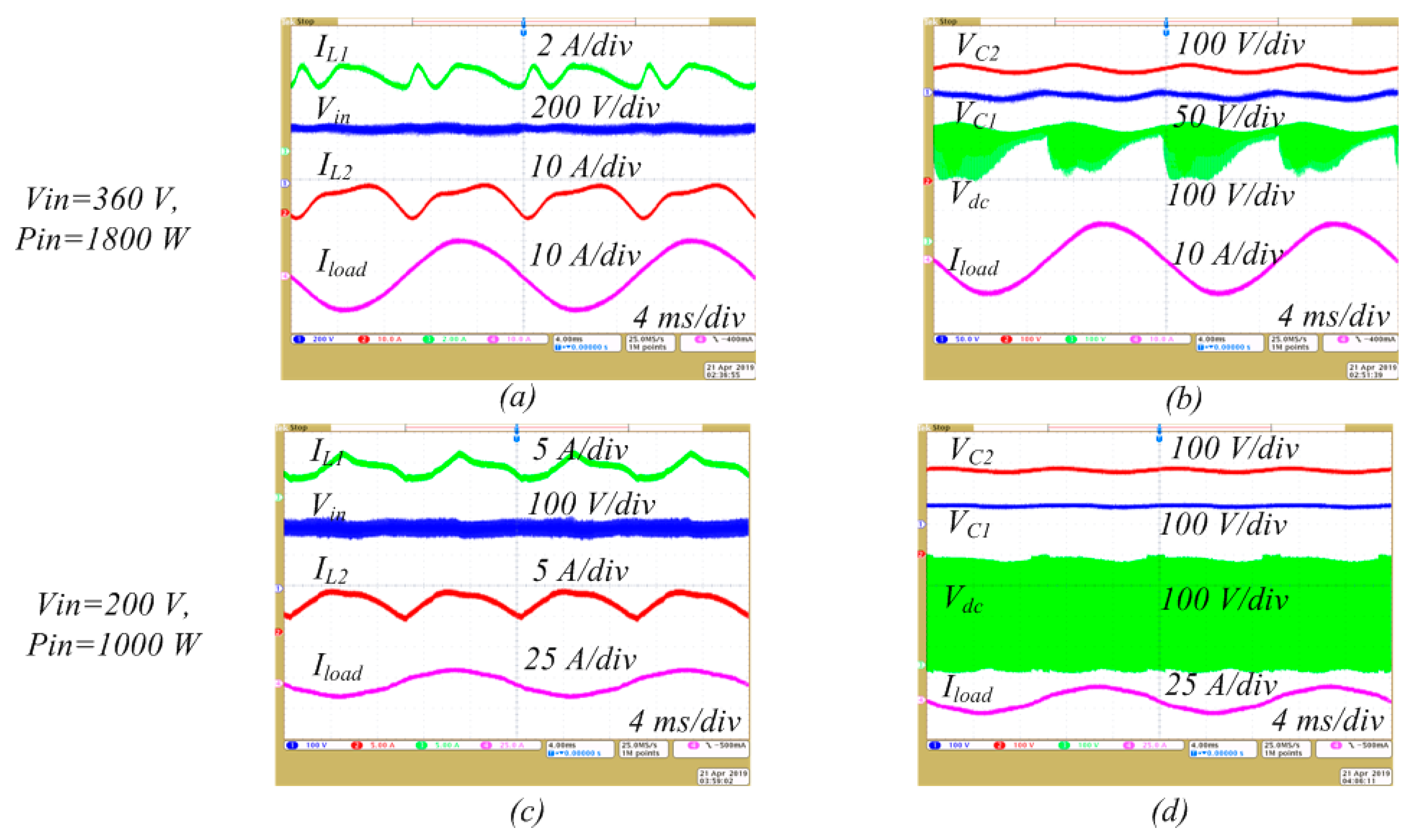
4.2. Operation Waveforms and Characteristics of the Prototypes

The experimental waveforms are shown below in Figure 6 and Figure 7 for both the 2L QZSI and the 3L NPC QZSI. Figure 6 shows the experimental results in the open loop mode of the 2L QZSI. Figure 6a,b correspond to the nominal power point 1800 W with the input voltage 360 V. The operation in the boost mode (power point of 1 kW) is presented in Figure 6c,d. To boost input voltage of 200 V up to 360 V at DC-link, the duty cycle DS = 0.225 was applied. The impact of the ST states on the ripples can be observed.
The appropriate waveforms for 3l NPC QZSI are depicted in Figure 7.
The diagrams presented are similar. The LF ripple of the input current was about 30% for both solutions that slightly exceeded the analytically calculated level of 25%. However, the input currents for both converters were in the CCM and the HF ripples for the 2L QZSI and the 3L NPC QZSI corresponded to the calculated value of 8%. The voltage ripples at C1 are 1.5–1.6% and ripples at C2 were 1.2–1.4%, which completely satisfied or nearly the calculated values of 2% and 1%, correspondingly.
In addition, Figure 8 shows the experimental diagrams of the PV-inverter operation in the closed-loop grid-connected mode for the nominal and reduced input power. It can be observed that the input current ripples had an LF ripple that corresponded to the double-frequency ripple. In the second case (Figure 8b), the current ripple had an HF component. It should be noted that a closed-loop system stabilizes the behavior of the converter. The observed current ripples completely corresponded to the theoretical expectation.

4.3. Efficiency Evaluation

Figure 9a shows the efficiency dependencies versus the input power. It corresponded to the different irradiance levels of the PV-string. It means that different operation points corresponded to the different input voltages and input currents. Since PV inverters are not operating at a nominal power point constantly, the important characteristics of the PV inverter performance is the weighted CEC efficiency [46]. The value of the weighted CEC efficiency was obtained by assigning a probable percentage of time the inverter resides at a certain operating point. If we denote the efficiency at 50% of the nominal power by “Eff50%”, the average EU (European) and CEC efficiency values weighted appropriately are defined as:
η E U =   0.03 · Eff 5 %   +   0.06 · Eff 10 %   +   0.13 · Eff 20 %   +   0.10 · Eff 30 %   +   0.48 · Eff 50 %   +   0.20 · Eff 100 % ,
η C E C =   0.04 · Eff 10 %   +   0.05 · Eff 20 %   +   0.12 · Eff 30 %   +   0.21 · Eff 50 %   +   0.53 · Eff 75 %   +   0.05 · Eff 100 % ,
The CEC efficiency measurement and calculation results corresponding to Figure 9a are shown in Table 4. For both inverters, it exceeds 96%. However, for the 2L QZSI it supersedes by 0.4%. The EU efficiency was also measured and for both converters it exceeded 95%.
It should be mentioned that efficiency curves for the 2L QZSI and the 3L NPC QZSI are characterized by different shapes. Figure 9b shows efficiency dependence versus different input voltage. This case illustrates the efficiency of the converters with different numbers of PV panels or at shadowed conditions. It can be seen that the 2L solution had higher peak efficiency, which corresponds to the nominal operation point, but more significant efficiency decrease occurred at low input voltage. In general, for the zero ST duty cycle, the 2L QZSI demonstrated 0.4…2.3% higher efficiency than the 3L NPC QZSI. The situation changed when a non-zero ST duty cycle was utilized. It can be explained by higher conduction losses in SiC transistors, which take force under higher current rates in ST mode.

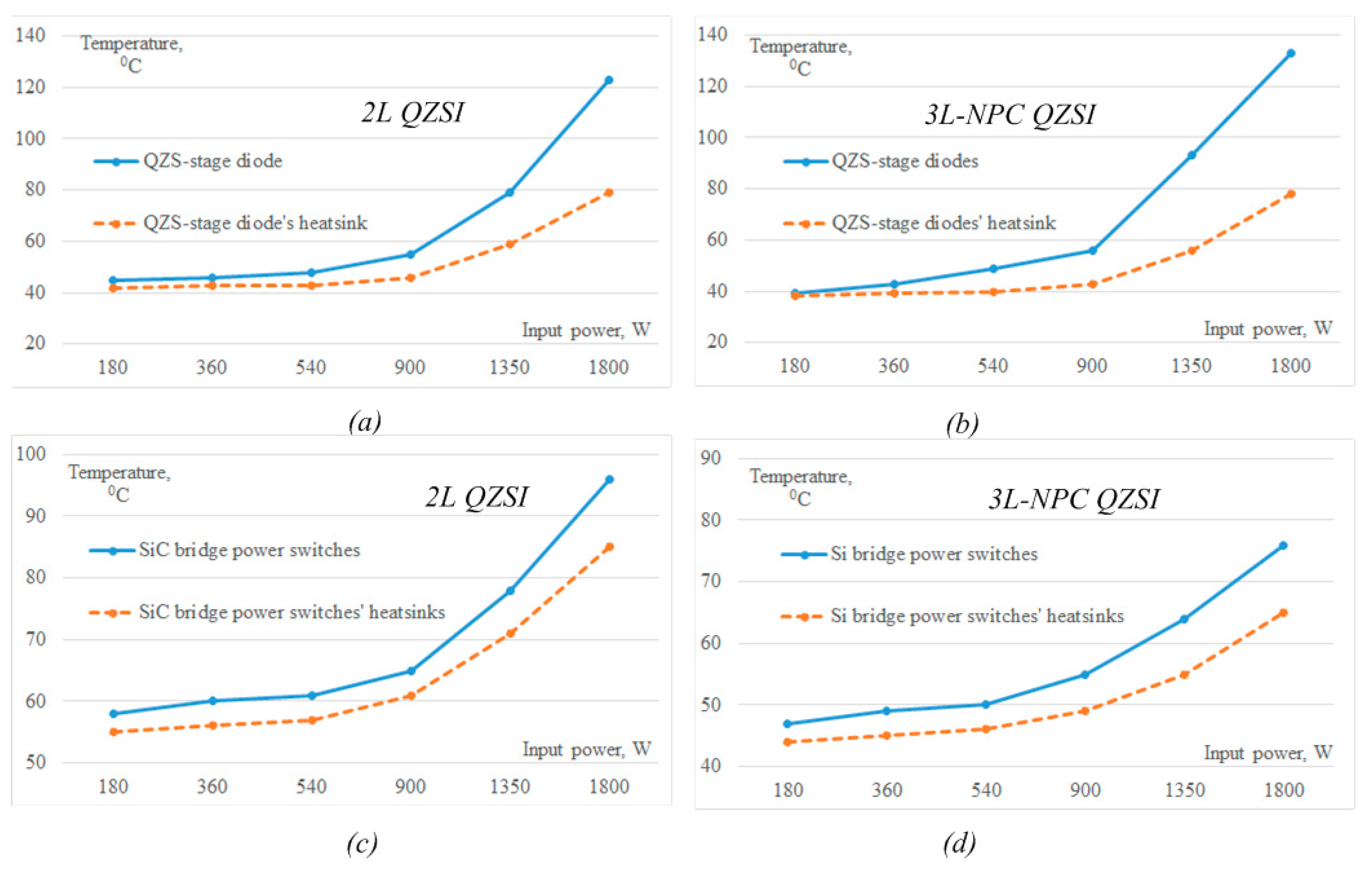
4.4. Evaluation of Temperature Behavior of Semiconductors and Heatsinks

The temperature of semiconductor devices and heatsinks was controlled by an infrared thermal camera Fluke Ti10. The results are presented in Figure 10 and Figure 11. It should be mentioned that clamping diodes and inverter power switches in the 3L NPC QZSI had four common heatsinks, each one intended for two MOSFETs and one clamping diode. One more heatsink was used for two QZS-stage diodes, as can be seen from Figure 5. At the same time, two heatsinks were used in the 2L QZSI for inverter switches and one heatsink for the QZS-stage diode.
Figure 10a shows the temperature of the QZS-stage diode and its heatsink in the 2L QZSI under different power levels. These points correspond to Figure 9a. It can be seen that the diode and the heatsink temperature rose under the power increase. The maximum temperature corresponded to the maximum power and fully corresponded to the theoretical assumptions. Figure 10b shows the temperature of the QZS-stage diodes and their heatsink in the 3L NPC QZSI under different power levels. It can be seen that the diode and heatsink temperature was slightly higher than in the 2L solution. The thermal images of the QZS-stage diode D1 at close to nominal power level (1850 W) are shown in Figure 11a,c. For the 2L QZSI and 3L NPC QZSI, the hottest points were the temperatures 130 °C and 140 °C, respectively.
Figure 10c,d show similar diagrams for SiC power switches in the 2L QZSI and Si power switches in the 3L NPC QZSI. The maximum temperature of the SiC power switches in the nominal mode was not higher than 95 °C in the 2L QZSI, while the maximum temperature of the Si power switches in the 3L NPC QZSI was much lower and did not exceed 75 °C. It should be mentioned, that under the ST states application in the boost mode, the temperature of the bridge power switches rose significantly in both cases.
In the case of the 2L solution, the SiC temperature reaches 160 °C, while in the 3L NPC solution the Si temperature did not exceed 120 °C at the maximum power points. Figure 11b,e show the SiC thermal pictures for two modes at the same power point of 1850 W. It can be seen that under the transient from nominal to boost mode, the temperature of the QZS-stage diodes changed insignificantly in both solutions.
The SiC power switches temperature in the 2L solution rose from 90…110 °C to 130…160 °C, while in the 3L solution based on the Si power switches, the temperature rose from 70…80 °C to 100…110 °C only. Finally, the SiC semiconductor devices can safely operate with higher temperature. It means that the size of the heatsinks in the case of full-SiC design can be smaller.

5. Comparative Analysis

This section presents the results of the comparison of different characteristics discussed and verified above. Figure 12 shows a diagram that includes several parameters for the 2L QZSI and the 3L NPC QZSI: volume of capacitors, volume of inductors, summarized voltage stress across semiconductors, heatsink volume, and CEC efficiency.
As can be seen, the equivalent inductances and capacitances of the QZS-stage are practically equal. It is explained by the same operation conditions of the proposed solutions and the same switching frequency. In the case of the 3L NPC, the capacitors and inductors are split, but the overall size remains the same.
The main difference concerns semiconductors. Overall voltage stress across full bridge transistors remains the same, but the 3L NPC requires additional clamping diodes. It was also clearly shown, that due to the higher operation temperature of the SiC devices in 2L QZSI, the heatsink can be selected significantly smaller.
Finally, the diagram also shows that power losses (1-CEC) are slightly smaller in the 2L QZSI than in the 3L NPC QZSI. It was achieved even under the higher operation temperature of SiC semiconductors.

6. Conclusions

In this study, a PV-string with a nominal power level of 1800 W was chosen as a case study for the evaluation of two PV-inverters based on the 2L QZSI full-SiC solution and the 3L NPC QZSI solution with Si MOSFETs. However, both investigated topologies could be easily up-scaled (with appropriately selected passive components) and safely operated up to twice the higher power level. The main conclusion from our analysis is that the full-SiC 2L QZSI solution has a clear advantage over the 3l NPC QZSI solution with Si MOSFETs. First of all, it simplifies the Printed Circuit Board (PCB) and reduces the number of auxiliary components around switches. Secondly, it may provide higher efficiency along with the lower volume of heatsink. It should be mentioned that efficiency and heatsink volume can be used as trade-off parameters for industrial optimization. The heatsink volume increase will lead to the temperature decreasing and to efficiency improvements correspondingly. On the other hand, the reliability and longtime operation of the full-SiC solution is an open question for discussion and can be a limiting factor in industrial implementation.

Author Contributions

Conceptualization, S.S. and O.H.; methodology, S.S. and C.R.-C.; software, O.H. and S.S.; validation, S.S. and S.P.P.; formal analysis, S.S. and C.R.-C.; investigation, S.S. and E.S.; resources, D.V., O.H. and S.S.; data curation, S.S. and O.H.; writing—original draft preparation, S.S.; writing—review and editing, S.S., O.H. and D.V.; visualization, S.S.; supervision, D.V. and O.H.; project administration, O.H. and S.S.; funding acquisition, S.S.

Funding

This research was carried out with the support of the European Regional Development Fund and the programme Mobilitas Pluss under the project MOBJD126 awarded by the Estonian Research Council. This work was also supported by the Estonian Centre of Excellence in Zero Energy and Resource Efficient Smart Buildings and Districts (ZEBE), grant 2014-2020.4.01.15-0016 funded by the European Regional Development Fund, and by the Estonian Research Council grant PUT1443.

Conflicts of Interest

The authors declare no conflict of interest.

References

  1. Ghosh, R.; Wang, M.; Mudiyula, S.; Mhaskar, U.; Mitova, R.; Reilly, D.; Klikic, D. Industrial Approach to Design a 2-kVa Inverter for Google Little Box Challenge. IEEE Trans. Ind. Electron. 2018, 65, 5539–5549. [Google Scholar] [CrossRef]
  2. Tang, Y.; Yao, W.; Loh, P.C.; Blaabjerg, F. Highly reliable transformerless photovoltaic inverters with leakage current and pulsating power elimination. IEEE Trans. Ind. Electron. 2016, 63, 1016–1026. [Google Scholar] [CrossRef]
  3. Kjaer, S.B.; Pedersen, J.K.; Blaabjerg, F. A Review of Single-Phase Grid-Connected Inverters for Photovoltaic Modules. IEEE Trans. Ind. Appl. 2005, 41, 1292–1306. [Google Scholar] [CrossRef]
  4. Peng, F.Z. Z-Source Inverter. IEEE Trans. Ind. Appl. 2003, 39, 504–510. [Google Scholar] [CrossRef]
  5. Li, Y.; Anderson, J.; Peng, F.Z.; Liu, D. Quasi-Z-Source Inverter for Photovoltaic Power Generation Systems. In Proceedings of the 2009 Twenty-Fourth Annual IEEE Applied Power Electronics Conference and Exposition, Washington, DC, 15–19 February 2009; pp. 918–924. [Google Scholar] [CrossRef]
  6. Husev, O.; Roncero-Clemente, C.; Romero-Cadaval, E.; Vinnikov, D.; Stepenko, S. Single phase three-level neutral-point-clamped quasi-Z-source inverter. IET Power Electron. 2015, 8, 1–10. [Google Scholar] [CrossRef]
  7. Husev, O.; Blaabjerg, F.; Roncero-Clemente, C.; Romero-Cadaval, E.; Vinnikov, D.; Siwakoti, Y.P.; Strzelecki, R. Comparison of Impedance-Source Networks for Two and Multilevel Buck–Boost Inverter Applications. IEEE Trans. Power Electron. 2016, 31, 7564–7579. [Google Scholar] [CrossRef]
  8. Abdelhakim, A.; Davari, P.; Blaabjerg, F.; Mattavelli, P. Switching Loss Reduction in the Three-Phase Quasi-Z-Source Inverters Utilizing Modified Space Vector Modulation Strategies. IEEE Trans. Power Electron. 2017, 33, 4045–4060. [Google Scholar] [CrossRef]
  9. Roncero-Clemente, C.; Romero-Cadaval, E.; Pires, V.F.; Martins, J.F.; Vilhena, N.; Husev, O. Efficiency and Loss Distribution Analysis of the 3L Active NPC qZS Inverter. In Proceedings of the 2018 IEEE 12th International Conference on Compatibility, Power Electronics and Power Engineering (CPE-POWERENG 2018), Doha, Qatar, 10–12 April 2018; pp. 1–6. [Google Scholar] [CrossRef]
  10. Huang, S.; Zhang, Y.; Hu, S. Stator Current Harmonic Reduction in a Novel Half Quasi-Z-Source Wind Power Generation System. Energies 2016, 9, 770. [Google Scholar] [CrossRef]
  11. Wang, B.; Tang, W. A New CUK-Based Z-Source Inverter. Electronics 2018, 7, 313. [Google Scholar] [CrossRef]
  12. Priyadarshi, N.; Padmanaban, S.; Ionel, D.M.; Mihet-Popa, L.; Azam, F. Hybrid PV-Wind, Micro-Grid Development Using Quasi-Z-Source Inverter Modeling and Control—Experimental Investigation. Energies 2018, 11, 2277. [Google Scholar] [CrossRef]
  13. Wang, B.; Tang, W. A Novel Three-Switch Z-Source SEPIC Inverter. Electronics 2019, 8, 247. [Google Scholar] [CrossRef]
  14. Choi, W.-Y.; Yang, M.-K. Transformerless Quasi-Z-Source Inverter to Reduce Leakage Current for Single-Phase Grid-Tied Applications. Electronics 2019, 8, 312. [Google Scholar] [CrossRef]
  15. Husev, O.; Shults, T.; Vinnikov, D.; Roncero-Clemente, C.; Romero-Cadaval, E.; Chub, A. Comprehensive Comparative Analysis of Impedance-Source Networks for DC and AC Application. Electronics 2019, 8, 405. [Google Scholar] [CrossRef]
  16. Noman, A.; A Al-Shamma’a, A.; Addoweesh, K.; Alabduljabbar, A.; Alolah, A. Cascaded Multilevel Inverter Topology Based on Cascaded H-Bridge Multilevel Inverter. Energies 2018, 11, 895. [Google Scholar] [CrossRef]
  17. Hammami, M.; Rizzoli, G.; Mandrioli, R.; Grandi, G. Capacitors Voltage Switching Ripple in Three-Phase Three-Level Neutral Point Clamped Inverters with Self-Balancing Carrier-Based Modulation. Energies 2018, 11, 3244. [Google Scholar] [CrossRef]
  18. Wu, M.; Song, Z.; Lv, Z.; Zhou, K.; Cui, Q. A Method for the Simultaneous Suppression of DC Capacitor Fluctuations and Common-Mode Voltage in a Five-Level NPC/H Bridge Inverter. Energies 2019, 12, 779. [Google Scholar] [CrossRef]
  19. Tran, V.-T.; Nguyen, M.-K.; Ngo, C.-C.; Choi, Y.-O. Three-Phase Five-Level Cascade Quasi-Switched Boost Inverter. Electronics 2019, 8, 296. [Google Scholar] [CrossRef]
  20. Mookken, J.; Agrawal, B.; Liu, J. Efficient and Compact 50kW Gen2 SiC Device Based PV String Inverter. In Proceedings of the PCIM Europe 2014; International Exhibition and Conference for Power Electronics, Intelligent Motion, Renewable Energy and Energy Management, Nuremberg, Germany, 20–22 May 2014; pp. 1–7. [Google Scholar]
  21. Öztürk, S.; Canver, M.; Çadırcı, I.; Ermiş, M. All SiC Grid-Connected PV Supply with HF Link MPPT Converter: System Design Methodology and Development of a 20 kHz, 25 kVA Prototype. Electronics 2018, 7, 85. [Google Scholar] [CrossRef]
  22. Choi, W.-Y.; Yang, M.-K. High-Efficiency Design and Control of Zeta Inverter for Single-Phase Grid-Connected Applications. Energies 2019, 12, 974. [Google Scholar] [CrossRef]
  23. Guo, X.; Zhang, J.; Zhou, J.; Wang, B. A New Single-Phase Transformerless Current Source Inverter for Leakage Current Reduction. Energies 2018, 11, 1633. [Google Scholar] [CrossRef]
  24. Nguyen, M.-K.; Choi, Y.-O. Voltage Multiplier Cell-Based Quasi-Switched Boost Inverter with Low Input Current Ripple. Electronics 2019, 8, 227. [Google Scholar] [CrossRef]
  25. Nguyen, M.; Choi, Y. PWM Control Scheme for Quasi-Switched-Boost Inverter to Improve Modulation Index. IEEE Trans. on Power Electron. 2018, 33(5), 4037–4044. [Google Scholar] [CrossRef]
  26. Fernández, E.; Paredes, A.; Sala, V.; Romeral, L. A Simple Method for Reducing THD and Improving the Efficiency in CSI Topology Based on SiC Power Devices. Energies 2018, 11, 2798. [Google Scholar] [CrossRef]
  27. Wolski, K.; Zdanowski, M.; Rabkowski, J. High-frequency SiC-based inverters with input stages based on quasi-Z-source and boost topologies—Experimental comparison. IEEE Trans. Power Electron. 2019. [Google Scholar] [CrossRef]
  28. Tiku, D. Modular Multilevel MMI(HB) Topology for Single-Stage Grid Connected PV Plant. In Proceedings of the 11th IET International Conference on AC and DC Power Transmission, Birmingham, UK, 2015; pp. 1–8. [Google Scholar] [CrossRef]
  29. Keyhani, H.; Toliyat, H.A. Single-Stage Multistring PV Inverter With an Isolated High-Frequency Link and Soft-Switching Operation. IEEE Trans. Power Electron. 2014, 29, 3919–3929. [Google Scholar] [CrossRef]
  30. Strache, S.; Wunderlich, R.; Heinen, S. A Comprehensive, Quantitative Comparison of Inverter Architectures for Various PV Systems, PV Cells, and Irradiance Profiles. IEEE Trans. Sustain. Energy 2014, 5, 813–822. [Google Scholar] [CrossRef]
  31. Stepenko, S.; Roncero-Clemente, C.; Husev, O.; Makovenko, E.; Pimentel, S.P.; Vinnikov, D. New interleaved single-phase quasi-Z-source inverter with active power decoupling. In Proceedings of the 2018 IEEE 12th International Conference on Compatibility, Power Electronics and Power Engineering (CPE-POWERENG 2018), Doha, Qatar, 10–12 April 2018; pp. 1–6. [Google Scholar] [CrossRef]
  32. Makovenko, E.; Husev, O.; Romero-Cadaval, E.; Vinnikov, D.; Stepenko, S. Single-Phase Three-Level qZ-Source Inverter Connected to the Grid with Battery Storage and Active Power Decoupling Function. In Proceedings of the 2018 IEEE 59th International Scientific Conference on Power and Electrical Engineering of Riga Technical University (RTUCON), Riga, Latvia, 12–13 November 2018; pp. 1–6. [Google Scholar] [CrossRef]
  33. Stepenko, S.; Husev, O.; Pimentel, S.P.; Makovenko, E.; Vinnikov, D. Small Signal Modeling of Interleaved Quasi-Z-Source Inverter with Active Power Decoupling Circuit. In Proceedings of the 2018 IEEE 59th International Scientific Conference on Power and Electrical Engineering of Riga Technical University (RTUCON), Riga, Latvia, 12–13 November 2018; pp. 1–6. [Google Scholar] [CrossRef]
  34. Roncero-Clemente, C.; Husev, O.; Stepenko, S.; Romero-Cadaval, E.; Vinnikov, D. Interleaved single-phase quasi-Z-source inverter with special modulation technique. In Proceedings of the 2017 IEEE First Ukraine Conference on Electrical and Computer Engineering (UKRCON), Kiev, Ukraine, 29 May–2 June 2017; pp. 593–598. [Google Scholar] [CrossRef]
  35. Roncero-Clemente, C.; Stepenko, S.; Husev, O.; Romero-Cadaval, E.; Vinnikov, D. Maximum boost control for interleaved single-phase Quasi-Z-Source inverter. In Proceedings of the IECON 2017-43rd Annual Conference of the IEEE Industrial Electronics Society, Beijing, China, 29 October–1 November 2017; pp. 7698–7703. [Google Scholar] [CrossRef]
  36. Nguyen, M.-K.; Choi, Y.-O. Maximum Boost Control Method for Single-Phase Quasi-Switched-Boost and Quasi-Z-Source Inverters. Energies 2017, 10, 553. [Google Scholar] [CrossRef]
  37. Roncero-Clemente, C.; Stepenko, S.; Husev, O.; Miñambres-Marcos, V.; Romero-Cadaval, E.; Vinnikov, D. Three-Level Neutral-Point-Clamped Quasi-Z-Source Inverter with Maximum Power Point Tracking for Photovoltaic Systems. In Technological Innovation for the Internet of Things. DoCEIS 2013. IFIP Advances in Information and Communication Technology; Camarinha-Matos, L.M., Tomic, S., Graça, P., Eds.; Springer: Berlin/Heidelberg, Germany, 2013; Volume 394, pp. 334–342. [Google Scholar] [CrossRef]
  38. Pimentel, S.P.; Husev, O.; Stepenko, S.; Vinnikov, D.; Roncero-Clemente, C.; Makovenko, E. Voltage Control Tuning of a Single-Phase Grid-Connected 3L qZS-Based Inverter for PV Application. In Proceedings of the 2018 IEEE 38th International Conference on Electronics and Nanotechnology (ELNANO), Kiev, Ukraine, 24–26 April 2018; pp. 692–698. [Google Scholar] [CrossRef]
  39. Pimentel, S.P.; Husev, O.; Vinnikov, D.; Roncero-Clemente, C.; Stepenko, S. An Indirect Model Predictive Current Control (CCS-MPC) for Grid-Connected Single-Phase Three-Level NPC Quasi-Z-Source PV Inverter. In Proceedings of the 2018 IEEE 59th International Scientific Conference on Power and Electrical Engineering of Riga Technical University (RTUCON), Riga, Latvia, 12–13 November 2018; pp. 1–6. [Google Scholar] [CrossRef]
  40. Types of Solar Inverter Efficiency - Peak, Euro, and CEC-Solar Selections. Available online: http://www.solarselections.co.uk/blog/types-of-solar-inverter-efficiency-peak-vs-euro (accessed on 10 May 2019).
  41. SolarHub-PV Module Details: SPR-200-BLK-U-by SunPower. Available online: http://www.solarhub.com/product-catalog/pv-modules/764-SPR-200-BLK-U-SunPower (accessed on 13 May 2019).
  42. Husev, O.; Chub, A.; Romero-Cadaval, E.; Roncero-Clemente, C.; Vinnikov, D. Voltage Distortion Approach for Output Filter Design for Off-Grid and Grid-Connected PWM Inverters. J. Power Electron. 2015, 15, 278–287. [Google Scholar] [CrossRef] [Green Version]
  43. Model 62150h 600s/1000s-Chroma Systems Solutions. Available online: http://www.chromausa.com/pdf/Br-62150H-600S+1000S-dcsupply-112011.pdf (accessed on 24 May 2019).
  44. WT1800 High Performance Power Analyzer | Yokogawa Test & Measurement Corporation. Available online: https://tmi.yokogawa.com/us/solutions/products/power-analyzers/wt1800-high-performance-power-analyzer/ (accessed on 24 May 2019).
  45. MSO/DPO4000B Mixed Signal Oscilloscope | Tektronix. Available online: https://www.tek.com/oscilloscope/mso4000-dpo4000 (accessed on 24 May 2019).
  46. Cyclone IV Device Handbook-Intel. Available online: https://www.intel.com/content/dam/www/programmable/us/en/pdfs/literature/hb/cyclone-iv/cyclone4-handbook.pdf (accessed on 24 May 2019).
  47. Fluke Ti10 Infrared Camera | Fluke. Available online: https://www.fluke.com/en-us/product/thermal-cameras/ti10 (accessed on 27 May 2019).
  48. HM8118 LCR Bridge/Meter | Overview | Rohde & Schwarz. Available online: https://www.rohde-schwarz.com/pk/product/hm8118-productstartpage_63493-44101.html (accessed on 28 May 2019).
Figure 1. PV string characteristics and system power profile.
Energies 12 02509 g001
Figure 2. The 2L QZS inverter.
Energies 12 02509 g002
Figure 3. The 3l NPC QZS inverter.
Energies 12 02509 g003
Figure 4. The structure of the experimental verification setup.
Energies 12 02509 g004
Figure 5. Experimental prototypes of the 2L QZSI (a) and the 3L NPC QZSI (b).
Energies 12 02509 g005
Figure 6. Operation waveforms of 2L QZSI at a nominal power level of 1800 W (a,b) and in boost voltage mode at a reduced power level of 1000 W (c,d).
Energies 12 02509 g006
Figure 7. Operation waveforms of 3L NPC QZSI at a nominal power level of 1800 W (a,b) and in boost voltage mode at a reduced power level of 1000 W (c,d).
Energies 12 02509 g007
Figure 8. Grid-connected operation of 3L NPC QZSI at a nominal power level of 1800 W (a) and in boost voltage mode at a reduced power level of 900 W (b).
Energies 12 02509 g008
Figure 9. Efficiency evaluation of the 2L QZSI and the 3L NPC QZSI under different solar irradiance (power) levels (a) and within input voltage operating range (b).
Energies 12 02509 g009
Figure 10. Temperatures of the QZS-stage diode and heatsink in the 2L QZSI (a) and 3L NPC QZSI (b), temperatures of the SiC bridge power switches and heatsinks in the 2L QZSI (c), and temperatures of the Si bridge power switches and heatsinks in the 3L NPC QZSI (d).
Energies 12 02509 g010
Figure 11. Thermal images in the nominal operation mode: QZS-stage diode (a) and SiC bridge power switches (b) in the 2L QZSI and QZS-stage diode in the 3L NPC QZSI (c); thermal images in the boost mode under ST states application: QZS-stage diode (d) and SiC bridge power switches (e) in the 2L QZSI and QZS-stage diode in the 3L NPC QZSI (f).
Energies 12 02509 g011
Figure 12. Comparative diagram for the 2L QZSI and 3L NPC QZSI.
Energies 12 02509 g012
Table 1. Parameters and characteristics of existing solutions.
ReferencesInverter TopologyRated Power, kWInput Voltage, VSemiconductor Devices and Switching FrequencyOutput Rms Voltage and FrequencyPeak/CEC Efficiency, %
[1]SAF with
FB VSI
2450900 V SiC MOSFET/45 kHz
650V Si IGBT/45 kHz
240 V, 60 Hz97.75/97.2
97.0/96.4
[2]FB VSI0.5280Si MOSFET/19.2 kHz110 V, 60 Hz96/-
[4]3-Phase ZSI4.5150IGBT/10 kHz208 V, 60 Hz-/-
[5]3-Phase QZSI4.3189–400600 V diode &
600 V IGBT/10 kHz
208 V, 60 Hz-/-
[6]3l NPC QZSI1220–325600 V diode and
600 V Si MOSFET/100 kHz
230 V, 50 Hz94/-
[11]CUK-based ZSI0.4901200 V IGBT
K40T1202/20 kHz
110 V, 50 Hz-/-
[13]3-switch ZSI SEPIC0.51001200 V IGBT
K40T1202/20 kHz
124 V, 50 Hz91.7/-
[14]QZSI
+2 bi- directional switches
1250SiC diode C4D20120D and SiC MOSFET C2M0080120D/10 kHz
1200 V IGBT
IKW25T120/10 kHz
220 V, 60 Hz95.1/-
92.9/-
[20]Interleaved boost DC–DC + T-type 3L 3-phase DC–AC50450-8001.2kV SiC C4D20120D + 1.2kV SiC MOSFET C2M0025120D
+ 600V SiC C3D16060D + 1.2kV SiC MOSFET C2M0025120D/75 kHz
480 V, 50 Hz99.4/-
[21]HF link DC–AC–DC + 3-phase 2L VSI 25533SiC HB module CAS120M12BM2 + SiC diodes C4D40120D and 3 Phase SiC module CCS050M12CM2400 V, 50 Hz98.5/-
[22]Zeta
inverter
0.2248300 V MOSFET IXFK150N30P3 + 1200 V SiC MOSFET UJC1206k/50 kHz220 V, 60 Hz95/-
[24]QSBI0.3550–72Diodes STPS60SM200C and IXYS30-60A + MOSFETs IRFP4668 and IRFP460/20 kHz110 V, 50 Hz91.3/-
[25]QSBI0.458–100Diodes DSEP 30–06A + MOSFETs IRFP460/10 and 20 kHz110 V, 50 Hz94/-
[27]QZSI
BC+VSI
IBC+VSI
6400–6001 × C4D20120D diodes + 6 × C2M0080120D/100 kHz
1 × C4D20120D diodes + 1 × C2M0080120D + 6 × C2M0080120D/100 kHz
2 × C4D20120D diodes + 1 × C2M0080120D + 6 × C2M0080120D/100 kHz
220 V, 50 Hz95.97/-
95.96/-
96.11/-
Table 2. Photovoltaic (PV) panel and system parameters.
PV panel parametersValuesSystem parametersValues
Standard Test Conditions (STCs): Air Mass (AM) 1.5, Irradiance 1000 W/m², cell temperature 25 °CNominal power Pnom = 1800 W
Nominal voltageVnom = 200–400 V
Nominal power (+/−5%)Pnom = 200 WNominal currentInom = 5 A
Rated voltageVmpp = 40.0 VLoad RMS voltage Vload = 230 V
Rated currentImpp = 5.00 AOutput current THDTHDI < 3%
Open circuit voltage Voc = 47.8 VMin operating powerPmin = 90 W
Short circuit currentIsc = 5.40 AMax operating powerPmax = 2000 W
Nominal Operating Cell Temperature (NOCT): Air Mass (AM) 1.5, Irradiance 800 W/m², cell temperature 46 °C +/−2 °CMin operating voltageVmin = 180 V
Max operating voltageVmax = 480 V
Nominal powerPnom = 146 WVoltage rippleΔV < 5%
Rated voltageVmpp = 36.5 VMax input currentImax = 10 A
Rated currentImpp = 4.01 ACurrent rippleΔI < 10%
Open circuit voltage Voc = 44.5 VNumber of PV panels N = 5…10
Short circuit currentIsc = 4.38 ACase study PV panelsSPR-200-BLK
Table 3. Selected elements.
Components2L QZSI3l NPC QZSI
QZS-stage inductorsL1 = L2 = 1.8 mHL1 = L2 = L3 = L4 = 0.9 mH
QZS-stage capacitorsEKMS3B1VSN122MA50S,
C1 = 1200 µF, 105 °C, 315 V,
3000 Hrs, 3.25 A,
ESR 100 mΩ;
ALC10(1)681DL500,
C2 = 680 µF, 85 °C, 500 V,
2000 Hrs, 3.65 A,
ESR 244 mΩ
ESMQ201VSN122MQ40S, C1 = C4 = 1200 µF, 85 °C, 200 V, 2000 Hrs, 3.5 A, ESR 166 mΩ;
B43504G2158M80, C1 = C4 = 1500 µF, 105 °C, 200 V, 3000 Hrs, 3.4 A, ESR 100 mΩ;
B43545C9397M000, C2 = C3 = 390 µF, 105 °C, 400 V, 5000 Hrs, 2.3 A, ESR 150 mΩ;
LPW471M2GQ45M, C2 = C3 = 470 µF, 85 °C, 400 V, 2000 Hrs, ESR 420 mΩ
Output filterLF1 = 0.56 mH, LF2 = 0.2 mH, CF = 15 µF
QZS-stage and clamping diodesD1: SiC C4D02120A, VRRM = 1200 VD1–D6: SiC C3D10065A, VRRM = 650 V
Inverter bridge switchesS1–S4: C2M0080120D MOSFETs SiC, VDS = 1200 V, RDS = 80 mΩS1–S8: IPW65R041CFD MOSFETs Si
, VDS = 650 V, RDS = 41 mΩ
Gate driversACPL-H342 (2.5 A max peak output current)
Table 4. The CEC efficiency of 2L QZSI and 3L NPC QZSI.
Power Checkpoints, % of NominalInput Power, W2L QZSI Efficiency, %3l NPC QZSI Efficiency, %
1018090.890.0
2036094.994.0
3054096.295.7
5090097.096.6
75135097.196.8
100180096.596.1
-CEC efficiency96.696.2

