Article

Ripple Vector Cancellation Modulation Strategy for Single-Phase Quasi-Z-Source Inverter

School of Automation, Central South University, Changsha 410083, China
*
Author to whom correspondence should be addressed.
Energies 2019, 12(17), 3344; https://doi.org/10.3390/en12173344
Submission received: 6 August 2019 / Revised: 21 August 2019 / Accepted: 23 August 2019 / Published: 30 August 2019

Abstract

:
The double-frequency (2ω) power flows through the DC side of the single-phase quasi-Z-source inverter (QZSI) leads to the 2ω voltage ripple of capacitors and 2ω current ripple of inductors. This paper proposes a ripple vector cancellation modulation strategy (RVCMS) based on the thought of ripple vector cancellation. By analyzing the mechanism of ripple generation and transmission, we can obtain a variation of a shoot-through duty cycle to generate a compensated 2ω ripple used to cancel the 2ω current ripple of inductors caused by the 2ω ripple of DC link current, and the 2ω compensated variation of a shoot-through duty cycle with a specific amplitude and phase is added to the constant shoot-through duty cycle. Finally, simulation and experimental results demonstrate the correctness and effectiveness of the proposed modulation strategy for the single-phase QZSI.

1. Introduction

The single-phase quasi-Z-source inverter (QZSI) consists of two modules, a quasi-Z-source network, and an H-bridge, and the quasi-Z-source network includes two inductors, two capacitors, and a diode [1]. Different from traditional two-stage inverters, the QZSI reduces the number of active devices, has no dead time, and can realize DC-DC and DC-AC by its unique impedance network and shoot-through modulation method [2,3]. Currently, the QZSI has been widely studied and applied in photovoltaic power generation, AC speed regulation, electric vehicles, and as a module in cascaded multilevel inverters [4,5,6,7].
For the single-phase inverter system, the double-frequency (2ω) power flows between the DC side, and the AC side causes 2ω ripples of capacitor and DC link voltage, 2ω ripples of inductor and DC link current. These 2ω ripples will cause the temperature of passive devices and the DC source to increase, which seriously affects their working life, distort the output voltage of the inverter, and the low frequency current ripple components in the DC side will affect the maximum power point tracking (MPPT) and reduce the efficiency of the photovoltaic system [8,9,10,11,12,13,14]. Therefore, it is necessary to suppress the 2ω ripple in the DC side. The simplest method to reduce the ripple is to increase the value of the quasi-Z-source network to buffer 2ω power in a large capacitor or inductor [8]. In [9], a parameter design method with a dynamic photovoltaic-panel and terminal capacitors for the single-phase quasi-Z-source photovoltaic inverter was proposed to reduce the 2ω ripple. However, these methods will not only lead to large volume, large weight and high cost, but also reduce reliability and efficiency due to the large value of capacitors and inductors in the quasi-Z-source network. In [10], a comprehensive model and an asymmetric quasi-Z-source network design method for a single-phase energy-stored quasi-Z-source-based photovoltaic inverter system were proposed to reduce the 2ω ripple.
The active power filter (APF) technology is usually applied to the ripple suppression for QZSI. In [11], an active-filter-integrated single-phase QZSI was proposed: The APF consists of an extra switch leg and a second-order filter; the 2ω pulsating power of the AC load is transferred to the filter and the extra leg; the capacitor voltage and the inductor current in the DC side will no longer have the 2ω ripple component with this method, but an extra circuit means a higher cost and more complicated control. In [12,13], 2ω ripple control strategies were proposed based on feed-back control. In [12], a low-pass filter was used to obtain the 2ω ripple of the inductor current in the DC side by extracting its DC component, which is used to generate a small variation of the shoot-through duty cycle, and Reference [13] regards the 2ω voltage ripple of the DC source as the feed-back signal. Reference [14] proposes a 2ω ripple suppression method based on feed-forward control: The feed-forward signal is obtained by a ripple observer, which can observe the 2ω current of the DC link by detecting the output current of the inverter. References [12,13,14] can realize the suppression of the 2ω ripple without an extra active filter circuit; we can call it virtual APF technology. However, they still need filters or sensors to detect the 2ω ripple components, which will increase the cost. Therefore, the relationship between the variation of the shoot-through duty cycle and the 2ω ripple in the DC side, and realizing the suppression of the 2ω ripple with less hardware, needs further study.
Reducing the modulation ratio of QZSI can effectively reduce the ripple content in the DC side; however, with the decrease of the modulation ratio and the increase of the shoot-through duty cycle, the harmonic distortion value of the inverter output voltage and the loss of switching devices will increase [15]. Some new modified modulation strategies have been addressed. In [16], a modified modulation strategy was proposed, which was different from the traditional modulation strategy; the shoot-through control lines are modified to a line with a 2ω component. Reference [17] proposes a novel dual switching frequency modulation that combines low-frequency sinusoidal pulse width modulation (SPWM) and high-frequency pulse width modulation (PWM) to remove the interdependence between the shoot-through duty cycle and the inverter modulation index. Reference [18] proposes two new space vector modulation strategies to reduce the inductor current ripple based on the principle of the volt-second balance, which can divide shoot-through times in real time. Reference [19] proposes a PWM strategy with a minimum inductor current ripple; the shoot-through time interval of three phase legs are designed according to the active state and 0 state time. In [20], a finite-control-set model-predictive control algorithm for a quasi-Z-source four-leg inverter based on the discrete time model and a predictive controller was proposed to minimize the 2ω ripple in the DC side. Reference [21] proposed a model-based current control approach based on the inherent relationship between the ripple component inductor and capacitor voltages in the DC side. This approach can reduce the DC side inductor current ripple with active damping and constant virtual time for single-phase grid-tied QZSI with an LCL filter.
This paper mainly focuses on the suppression of the 2ω current ripple of inductors and proposes a new modulation strategy based on ripple vector cancellation. In the modulation strategy, the compensated 2ω variation of the shoot-through duty cycle with a specific amplitude and phase angle is obtained to cancel the 2ω current ripple of inductors. Section 2 focuses on the operation analysis, ripple transmission, and generation mechanism of single-phase QZSI. Section 3 presents the proposed modulation strategy. Simulation and experimental studies are discussed in Section 4. Finally, conclusions are given in Section 5.

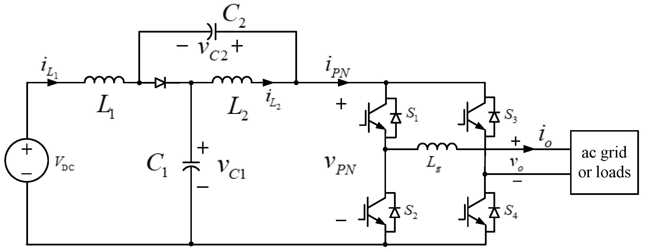
2. Single-Phase QZSI

2.1. Operation and Steady-State Analysis

The topology of single-phase QZSI is shown in Figure 1. Due to the existence of the quasi-Z-source network and the shoot-through state, both of the power switches in a leg can be turned on at the same time, which is used to step up the voltage. During the shoot-through state, the diode turns off, the inverter bridge is short circuited, the DC link voltage is 0, and the inverter does not generate the power to load. In the non-shoot-through state, the diode turns on, and the QZSI operates the same as a conventional voltage source inverter (VSI). In a switching period, the state-space model of QZSI can be obtained by using the state-space average method, as shown in (1), where i L 1 , i L 2 , v C 1 , and v C 2 are the current of inductors L 1 and L 2 , the voltage of the capacitors is C 1 and C 2 , v DC is the voltage of the DC source, d is the shoot-through duty cycle, and i P N is the DC link current, respectively.
Figure 2 shows the conventional modulation strategy (CMS) for the single-phase QZSI using the unipolar modulation strategy; its modulation waveforms are two sinusoidal waves with a difference of 180°. The CMS uses two straight lines v p , v n to generate the shoot-through duty cycle. When the triangular carrier is greater than v p , the switch S 1 or S 3 turns on, and when the carrier is smaller than v n , the switch S 2 or S 4 turns on. V S 1 and V S 2 show the switch state of the switch S 1 S 4 in the H-bridge, respectively.
{ L 1 d i L 1 d t = v DC ( 1 d ) v C 1 + d v C 2 L 2 d i L 2 d t = ( 1 d ) v C 2 + d v C 1 C 1 d v C 1 d t = ( 1 d ) ( i L 1 i P N ) d i L 2 C 2 d v C 2 d t = ( 1 d ) ( i L 2 i P N ) d i L 1
From (1), the DC components of the QZSI in the ideal case can be obtained as (2), where D is the average value of the shoot-through duty cycle d , d = D + d ^ , d ^ is the variation of d , V C 1 and V C 2 are the average voltage of capacitor C 1 and C 2 , I L 1 and I L 2 are the average current of inductor I L 1 and I L 2 , V DC is the average voltage of dc source, and I P N is the average value of the DC link current, respectively.
{ V C 1 = 1 D 1 2 D V DC V C 2 = D 1 2 D V DC I L 1 = I L 2 = 1 D 1 2 D I P N
The average value of the DC link voltage during the non-shoot-through time interval is
V P N = V C 1 + V C 2 = 1 1 2 D V DC

2.2. Ripple Genertation Mechanism

The output voltage and current of the single-phase QZSI inverter can be expressed as (4), where V o and I o are the amplitude of the output voltage and current, ω is the fundamental frequency, and φ is the impedance angle of the load or grid, respectively.
v o = V o sin ( ω t ) ,   i o = I o sin ( ω t φ )
The DC link voltage v P N and the DC link current i P N can be expressed as (5), where V P N , I P N are the average value and v ^ P N , i ^ P N are the 2ω components of v P N , i P N , respectively.
v P N = V P N + v ^ P N ,   i P N = I P N + i ^ P N
From (4) and (5), the input power p P N and output power p o of the H-bridge can be calculated as (6) and (7), respectively.
p P N = ( 1 D ) v P N i P N = ( 1 D ) ( V P N I P N + V P N i ^ P N + I P N v ^ P N + i ^ P N v ^ P N )
p o = 1 2 V o I o cos φ 1 2 V o I o cos ( 2 ω t φ )
The 2ω component of the DC link current can be given as (8), where I 2 ω is its amplitude and α is the phase angle.
i ^ P N = I 2 ω cos ( 2 ω t α )
From p P N = p o and Reference [12], the amplitude and phase angle of i ^ P N can be calculated as
I 2 ω = V o I o [ 4 ω 2 L C ( 1 2 D ) 2 ] 2 ( 1 D ) [ 4 ω 2 L C ( 1 2 D ) 2 ] 2 V P N 2 + [ 4 ω L I P N ( 1 D ) ] 2
α = φ + arctan 4 ω L I P N ( 1 D ) [ 4 ω 2 L C ( 1 2 D ) 2 ] V P N
In (9), 4 ω L I P N ( 1 D ) is much smaller than [ 4 ω 2 L C ( 1 2 D ) 2 ] V P N and can be ignored, therefore, the 2ω component of the DC link current can be expressed as
i ^ P N = V o I o 2 ( 1 D ) V P N cos ( 2 ω t α )
From (6) and (7), I P N can be calculated as
I P N = V o I o 2 ( 1 D ) V P N cos φ

2.3. Ripple Transmission Mechanism

When the shoot-through duty cycle is a variable value, from (1), the small-signal model of single-phase QZSI can be obtained as (13) using the small signal analysis method with a constant DC source voltage, where i ^ L 1 , i ^ L 2 , v ^ C 1 , v ^ C 2 are the 2ω components of the inductor current i L 1 , i L 2 , the capacitor voltage v C 1 , v C 2 , respectively.
{ L 1 d i ^ L 1 d t = ( 1 D ) v ^ C 1 + D v ^ C 2 + ( V C 1 + V C 2 ) d ^ L 2 d i ^ L 2 d t = ( 1 D ) v ^ C 2 + D v ^ C 1 + ( V C 1 + V C 2 ) d ^ C 1 d v ^ C 1 d t = ( 1 D ) i ^ L 1 D i ^ L 2 ( 1 D ) i ^ P N + ( I P N I L 1 I L 2 ) d ^ C 2 d v ^ C 2 d t = ( 1 D ) i ^ L 2 D i ^ L 1 ( 1 D ) i ^ P N + ( I P N I L 1 I L 2 ) d ^
The small signal model can be simplified as (14) under L 1 = L 2 = L and C 1 = C 2 = C , which means i ^ L = i ^ L 1 = i ^ L 2 and v ^ C = v ^ C 1 = v ^ C 2 referring to [8].
{ L d i ^ L d t = ( 1 2 D ) v ^ C + ( V C 1 + V C 2 ) d ^ C d v ^ C d t = ( 1 2 D ) i ^ L ( 1 D ) i ^ P N + ( I P N 2 I L 1 ) d ^
From (2), (3) and (14), the transmission mechanism model of the inductor current ripple (15) and capacitor voltage ripple (16) can be obtained with Laplace transforms.
i ^ L ( s ) = ( 1 2 D ) ( 1 D ) L C s 2 + ( 1 2 D ) 2 i ^ P N ( s ) + C s V DC + ( 1 2 D ) I P N ( 1 2 D ) [ L C s 2 + ( 1 2 D ) 2 ] d ^ ( s )
v ^ C ( s ) = ( 1 D ) L s L C s 2 + ( 1 2 D ) 2 i ^ P N ( s ) + ( 1 2 D ) V DC L s I P N ( 1 2 D ) [ L C s 2 + ( 1 2 D ) 2 ] d ^ ( s )
In (15), the transfer functions can be expressed as (17) and (18), where G i ^ P N i ^ L represents the transfer function of i ^ P N to i ^ L 1 , and G d ^ i ^ L represents the transfer function of d ^ to i ^ L .
G i ^ P N i ^ L ( s ) | d ^ = 0 = ( 1 D ) ( 1 2 D ) L C s 2 + ( 1 2 D ) 2
G d ^ i ^ L ( s ) | i ^ P N = 0 = C s V DC + ( 1 2 D ) I P N ( 1 2 D ) [ L C s 2 + ( 1 2 D ) 2 ]
From (2), (11), (12), (15), and (16), in the steady state, assuming a constant shoot-through duty cycle, we can get
{ i L 1 = I L 1 + i ^ L 1 = V o I o 2 ( 1 2 D ) V P N cos φ + ( 1 2 D ) V o I o 2 [ 4 ω 2 L C ( 1 2 D ) 2 ] V P N cos ( 2 ω t α ) i L 2 = I L 2 + i ^ L 2 = V o I o 2 ( 1 2 D ) V P N cos φ + ( 1 2 D ) V o I o 2 [ 4 ω 2 L C ( 1 2 D ) 2 ] V P N cos ( 2 ω t α ) v C 1 = V C 1 + v ^ C 1 = 1 D 1 2 D V DC + ω L V o I o [ 4 ω 2 L C ( 1 2 D ) 2 ] V P N sin ( 2 ω t α ) v C 2 = V C 2 + v ^ C 2 = D 1 2 D V DC + ω L V o I o [ 4 ω 2 L C ( 1 2 D ) 2 ] V P N sin ( 2 ω t α )
From (19), the 2ω current ripple ratios of i L 1 and i L 2 , the 2ω voltage ripple ratios of v C 1 and v C 2 can be defined as (20), (21), and (22), respectively.
a = | i ^ L 1 | I L 1 × 100 % = | i ^ L 2 | I L 2 × 100 % = ( 1 2 D ) 2 [ 4 L C ω 2 ( 1 2 D ) 2 ] cos φ × 100 %
b 1 = | v ^ C 1 | V C 1 × 100 % = ( 1 2 D ) ω L V o I o ( 1 D ) [ 4 ω 2 L C ( 1 2 D ) 2 ] V P N V DC × 100 %
b 2 = | v ^ C 2 | V C 2 × 100 % = ( 1 2 D ) ω L V o I o D [ 4 ω 2 L C ( 1 2 D ) 2 ] V P N V DC × 100 %

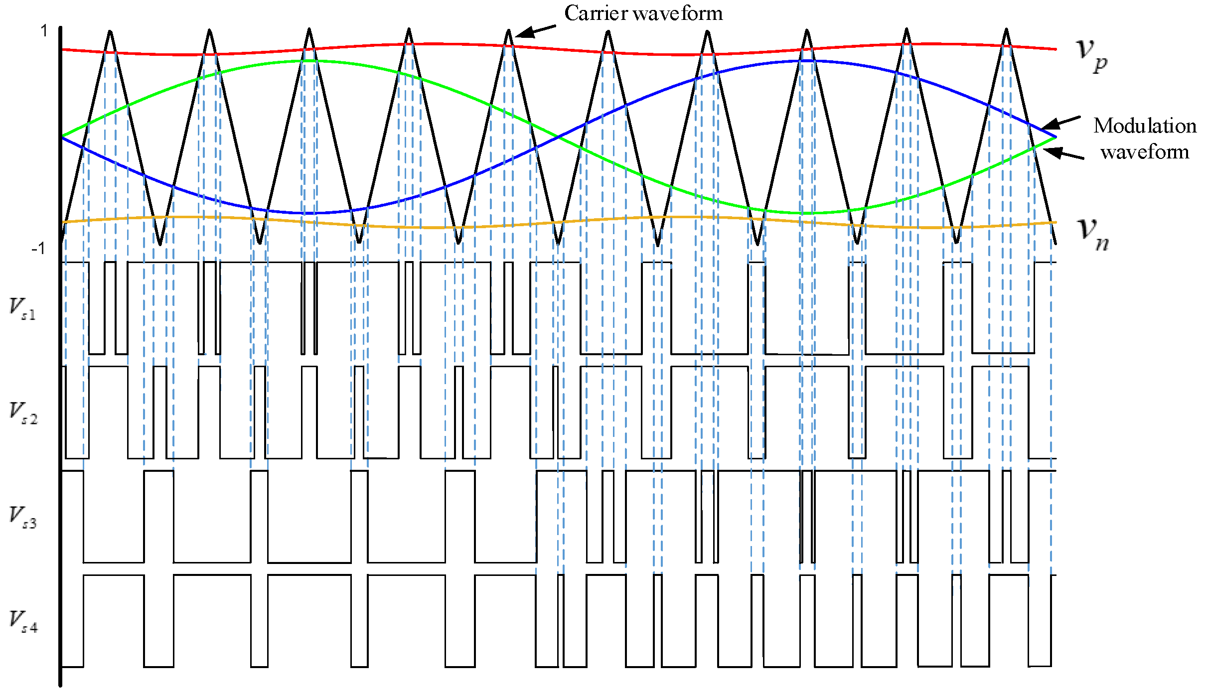
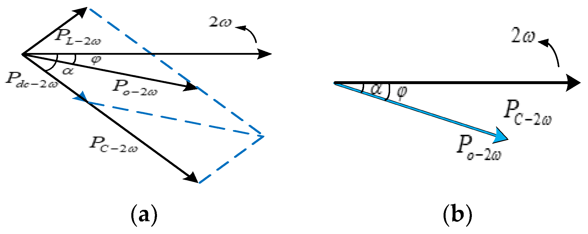
3. Modulation Strategy Based on Ripple Vector Cancellation

The ripple transmission models (15) and (16) show that the 2ω inductor current ripple and the capacitor voltage ripple in the DC side are related to the variation i ^ P N and d ^ . If the shoot-through duty cycle or the DC link current has a variation, the current of the inductors will contain variation i ^ L * and v ^ C * . This paper mainly focuses on the reducing of the 2ω current ripple in the DC side. Therefore, regarding i ^ L * caused by i ^ P N as the disturbance, which caused by d ^ as the compensation, theoretically, the 2ω current ripple will be suppressed to 0 with an appropriate d ^ . A 2ω shoot-through duty cycle d ^ = d ^ 2 ω with specific amplitude and phase angle, according to the magnitude of the 2ω inductors current ripple, can then be calculated based on the thought of the ripple vector cancellation. Adding the 2ω compensation variation d ^ 2 ω to the constant shoot-though duty cycle D , at this time, the shoot-through duty cycle can be expressed as
d = D + d ^ 2 ω
From (23), the shoot-through duty cycle consists of a constant value and a 2ω component, where D is determined by the output voltage of the inverter and the DC source voltage and d ^ 2 ω is determined by the actual 2ω current ripple in the DC side. Different from the CMS, as shown in Figure 3, the proposed ripple vector cancellation modulation strategy (RVCMS) uses two sine waveforms with 2ω components to generate the shoot-through duty cycle, where v p = 1 d and v n = 1 + d .
The 2ω compensated shoot-through duty cycle can be expressed as (24).
d ^ 2 ω = A sin ( 2 ω t + β )
From (17) and (18), the transfer function of i ^ P N to d ^ used to cancel the 2ω current ripple of inductors can be calculated as
G ( s ) = G i ^ P N i ^ L ( s ) G d ^ i ^ L ( s ) = ( 1 D ) ( 1 2 D ) 2 C s V DC + ( 1 2 D ) I P N
and d ^ 2 ω can be calculated by (26), where represents the convolution.
d ^ 2 ω = i ^ P N L 1 [ G ( s ) ]
From (3), (10), (11), (24)–(26), the amplitude A and phase angle β of d ^ 2 ω can be calculated as
A = V o I o ( 1 2 D ) 3 2 V DC 4 ω 2 C 2 V DC 2 + I P N 2 ( 1 2 D ) 2
β = arctan [ ( 1 2 D ) I P N 2 ω C V DC ] arctan ( 1 2 D ) ( 1 D ) 4 ω L I P N [ 4 ω 2 L C ( 1 2 D ) 2 ] V DC φ
When the proposed d ^ 2 ω is applied, the entire 2ω power is buffered by the capacitors and there is no 2ω power in the inductors and DC source. It should be noted that the 2ω voltage ripple of capacitors will reduce slightly when the 2ω current ripple of the inductors are limited to 0. The phasor diagram of the 2ω power flows with a different modulation strategy are shown in Figure 4, where P L 2 ω , P C 2 ω , P d c 2 ω , and P o 2 ω express the 2ω power of two inductors, two capacitors, and DC source and loads, respectively; the derivation and demonstration are given in Reference [12].

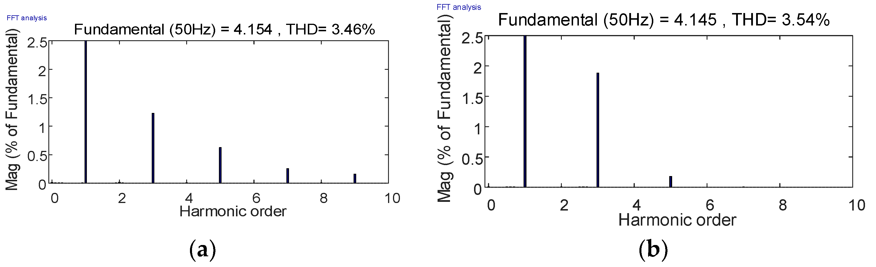
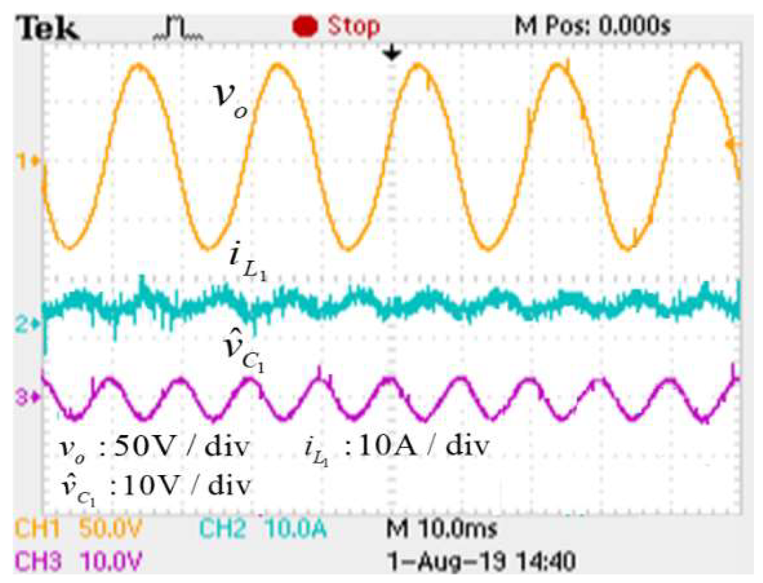
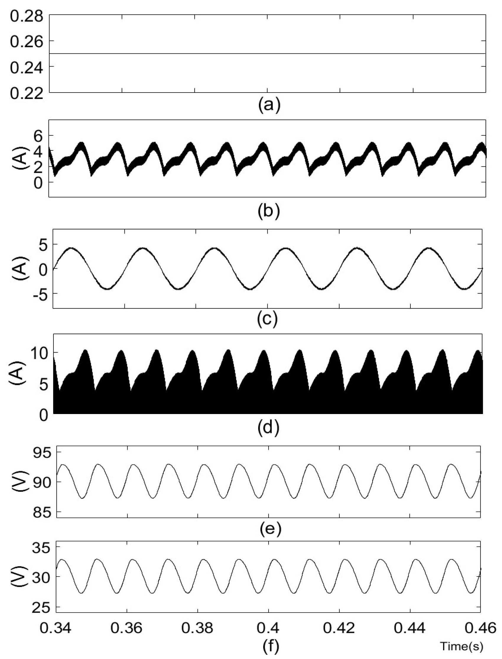
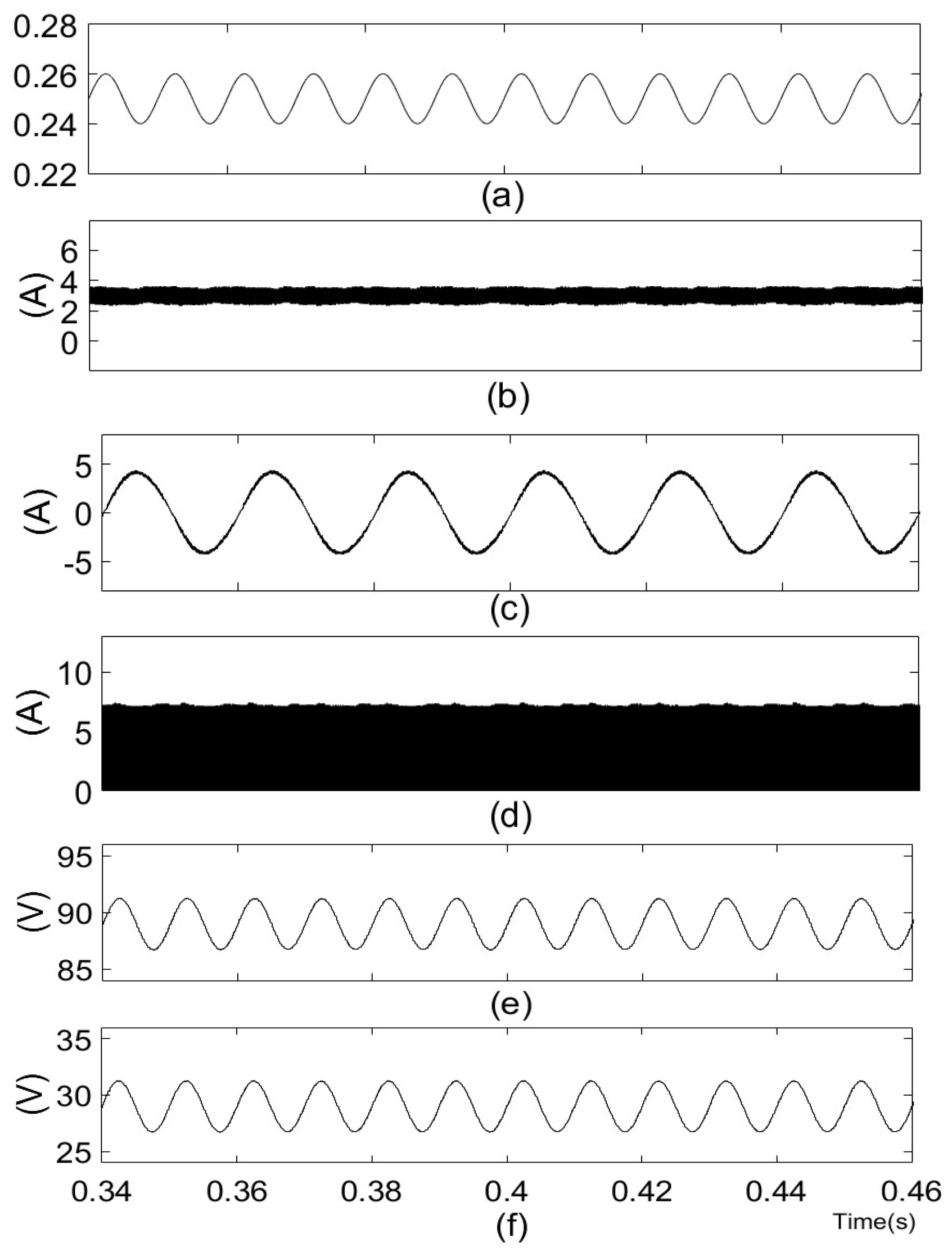
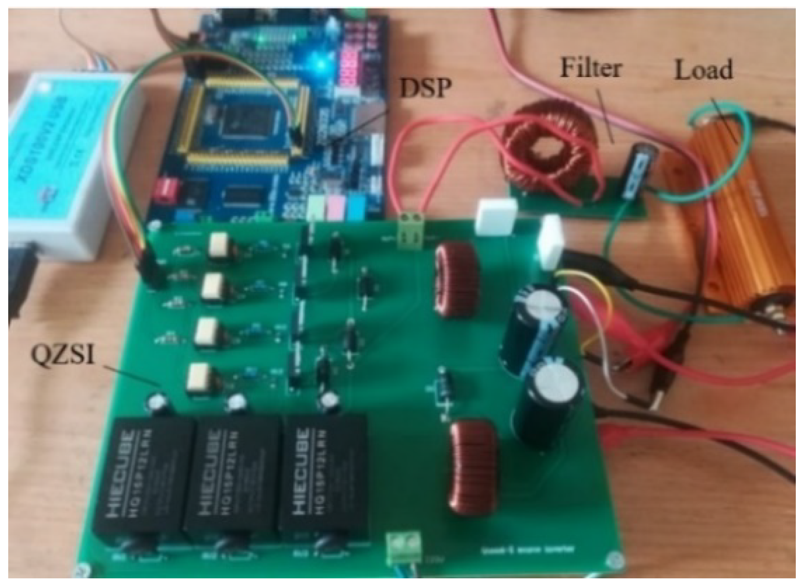
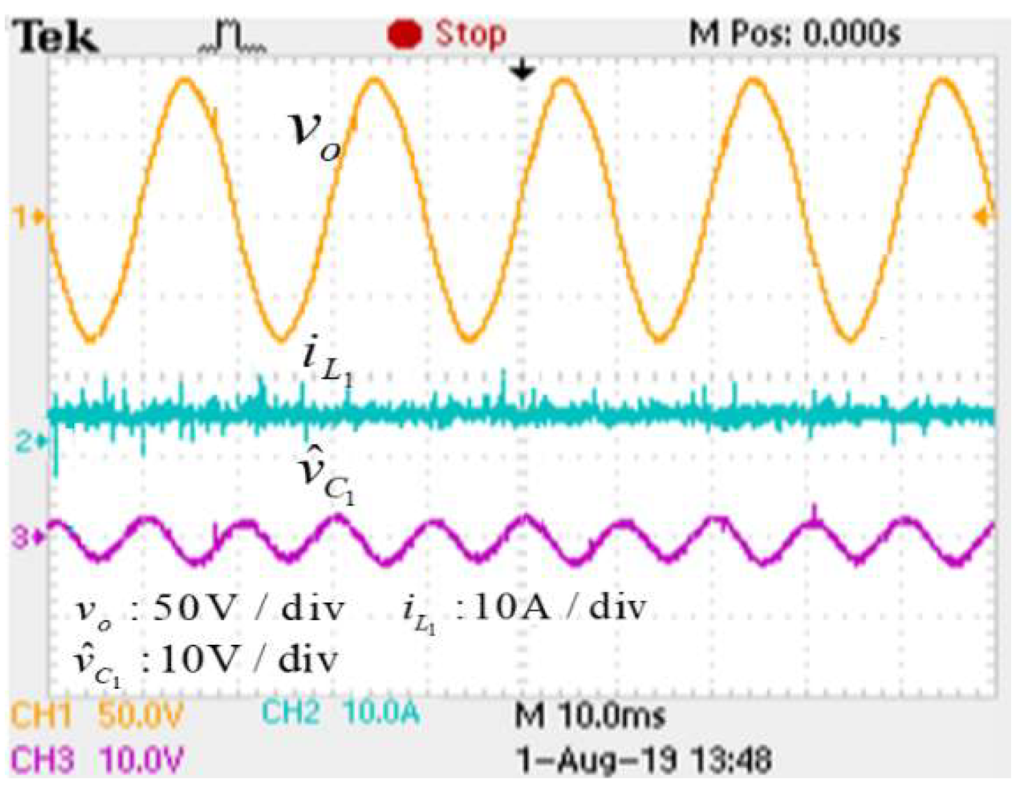
4. Simulation and Experimental Results

In order to verify the correctness and demonstrate the effectiveness of the proposed modulation strategy for the ripple suppression effect, the 2ω inductor current ripple must be large enough with the CMS, and in Reference [8] the simulation model was built, and its parameters are shown in Table 1. Figure 5 shows the simulation waveforms of d (a), i L 1 (b), i o (c), i P N (d) v C 1 (e), and v C 2 (f) with the CMS. The average values of i L 1 , i P N , v C 1 , and v C 2 are 3.014 A, 3.022 A, 90.21 V, and 30.21 V, and the amplitude of i o is 4.154 A, respectively. From Figure 5a, the shoot-through duty cycle is a constant; Figure 5b,d–f show the 2ω ripple of the inductor current and the DC link current, the capacitor voltage are quite large with the CMS.
Figure 6 shows the simulation results of d (a), i L 1 (b), i o (c), i P N (d), v C 1 (e), and v C 2 (f) with the RVCMS. With the proposed modulation strategy, the shoot-through duty cycle is a sine wave with a 2ω component; the current of inductor and the DC link have a little 2ω ripple. Figure 6e,f show the 2ω voltage ripple of capacitors reduced slightly compared to Figure 5e,f. The average values of i L 1 , i P N , v C 1 , and v C 2 are 2.993 A, 2.995 A, 88.98 V, and 28.98 V, and the amplitude of i o is 4.145 A, respectively. The simulation results show that the proposed RVCMS can effectively suppress the 2ω current ripple of inductors and can suppress the capacitor voltage ripple slightly compared to the CMS.
Table 2 lists the 2ω ripple ratios with the CMS and RVCMS. It can be seen that the 2ω inductor current ripple ratios decreased from 40.15% to 1.69%; the 2ω voltage ripple ratios of v C 1 decreased from 3.14% to 2.53%, and v C 2 decreased from 9.40% to 7.75%. If low 2ω ripple ratios in the DC side with the CMS are required, the large inductance and capacitance are necessary. From (20) and (21), assuming that a = 1.69 % and b 1 = 2.53 % , the inductance and capacitance of quasi-Z-source network will be L = 36.89   mH and C = 1.03   mF , respectively, and the inductance is much larger than the value with the RVCMS, achieving the same ripple suppression effect. Figure 7 shows the FFT spectrum of the AC output current with the CMS and the RVCMS, and the total harmonic distortion (THD) are 3.46% and 3.54%, respectively. It can be seen that the proposed RVCMS has little effect on the output power quality.
A single-phase QZSI experimental prototype was built in the laboratory, as shown in Figure 8. The PWM control signals of the proposed RVCMS and CMS for switches were generated by a TMS320F28335 DSP. Figure 9 and Figure 10 show the experimental results with the CMS and RVCMS, respectively. The experimental results show that the 2ω current ripple of inductors reduced greatly and the 2ω ripple of capacitors reduced slightly with the RVCMS compared to the CMS. Simulation and experimental results verify that the proposed RVCMS can realize the suppression of 2ω ripples in addition to the functions of the DC-AC and voltage boost for the single-phase QZSI.

5. Conclusions

This paper proposed a minimum 2ω inductor current ripple modulation strategy based on the thought of ripple vector cancellation. The ripple generation and transmission mechanism models for single-phase QZSI are built, which reveals the causes of the 2ω ripple in the DC side. The 2ω-compensated variation of the shoot-through duty cycle used to cancel the 2ω ripple of inductors was obtained and added to the constant shoot-through duty cycle. The proposed modulation strategy in this paper can effectively reduce the 2ω current ripple of inductors and slightly reduce the 2ω voltage ripple of capacitors without adding any active or passive filter branches, and a small value of inductors and capacitors are used to receive the same effect of the ripple suppression compared to the CMS. Some comparative evaluation of simulation and experimental results demonstrated the effectiveness and validity of the proposed RVCMS for the 2ω ripple suppression of single-phase QZSI.

Author Contributions

Y.T., conceptualization, methodology, and writing—original draft; Z.L., resources and writing—review and editing; Y.C., supervision and technical analysis; R.W., formal analysis and investigation.

Funding

This research was funded by Fundamental Research Funds for the Central Universities of Central South University Central South University, grant number: 502211922.

Conflicts of Interest

The authors declare no conflict of interest.

References

  1. Li, Y.; Anderson, J.; Peng, F.Z.; Liu, D. Quasi-z-source inverter for photovoltaic power generation systems. In Proceedings of the 2009 Twenty-Fourth Annual IEEE Applied Power Electronics Conference and Exposition, Washington, DC, USA, 15–19 February 2009; pp. 918–924. [Google Scholar]
  2. Anderson, J.; Peng, F.Z. Four quasi-Z-source inverters. In Proceedings of the IEEE Power Electronics Specialists Conference, Rhodes, Greece, 15–19 June 2008; pp. 2743–2749. [Google Scholar]
  3. Ayad, A.; Kennel, R. A comparison of quasi-Z-source inverters and conventional two-stage inverters for PV applications. EPE J. 2017, 27, 43–59. [Google Scholar] [CrossRef]
  4. Battiston, A.; Martin, J.P.; Miliani, E.H.; Nahid-Mobarakeh, B.; Pierfederici, S.; Meibody-Tabar, F. Comparison criteria for electric traction system using Z-source/quasi Z-source inverter and conventional architectures. IEEE J. Emerg. Sel. Top. Power Electron. 2014, 2, 467–476. [Google Scholar] [CrossRef]
  5. Battiston, A.; Miliani, E.H.; Pierfederici, S.; Meibody-Tabar, F. Efficiency improvement of a quasi-Z-source inverter-fed permanent-magnet synchronous machine-based electric vehicle. IEEE Trans. Transp. Electrific. 2016, 2, 14–23. [Google Scholar] [CrossRef]
  6. Liu, Y.; Ge, B.; Abu-Rub, H.; Peng, F.Z. An effective control method for quasi-Z-source cascade multilevel inverter-based grid-tie single-phase photovoltaic power system. IEEE Trans. Ind. Informat. 2014, 10, 399–407. [Google Scholar] [CrossRef]
  7. Liang, W.H.; Liu, Y.; Ge, B.; Wang, X.L. DC-Link voltage balance control strategy based on multidimensional modulation technique for quasi-Z-source cascaded multilevel inverter photovoltaic power system. IEEE Trans. Ind. Informat. 2018, 14, 4905–4915. [Google Scholar] [CrossRef]
  8. Sun, D.; Ge, B.; Yan, X.; Bi, D.; Zhang, H.; Liu, Y.; Abu-Rub, H.; Ben-Brahim, L.; Peng, F. Modeling, impedance design, and efficiency analysis of quasi-Z-source module in cascade multilevel photovoltaic power system. IEEE Trans. Ind. Electron. 2014, 61, 6108–6117. [Google Scholar] [CrossRef]
  9. Liu, Y.; Ge, B.; Abu-Rub, H.; Sun, D. Comprehensive modeling of single-phase quasi-Z-source photovoltaic inverter to investigate low-frequency voltage and current ripple. IEEE Trans. Ind. Electron. 2015, 62, 4194–4202. [Google Scholar] [CrossRef]
  10. Liang, W.H.; Liu, Y.; Ge, B.; Abu-Rub, H.; Balog, R.S.; Xue, Y.S. Double-line-frequency ripple model, analysis, and impedance design for energy-stored single-phase quasi-Z-source photovoltaic system. IEEE Trans. Ind. Electron. 2018, 65, 3198–3209. [Google Scholar] [CrossRef]
  11. Ge, B.; Abu-Rub, H.; Liu, Y.; Balog, R.S.; Peng, P.Z. An active filter method to eliminate dc-side low-frequency power for a single-phase quasi-z-source inverter. IEEE Trans. Ind. Electron. 2016, 63, 4838–4848. [Google Scholar] [CrossRef]
  12. Ge, B.; Liu, Y.; Abu-Rub, H.; Balog, R.S.; Peng, F.Z.; McConnell, S.; Li, X. Current Ripple Damping Control to Minimize Impedance Network for Single-Phase Quasi-Z Source Inverter System. IEEE Trans. Ind. Inform. 2016, 12, 1043–1054. [Google Scholar] [CrossRef]
  13. Zhou, Y.; Li, H.; Li, H. A single-phase PV quasi-Z-source inverter with reduced capacitance using modified modulation and double-frequency ripple suppression control. IEEE Trans. Power Electron. 2016, 31, 2166–2173. [Google Scholar] [CrossRef]
  14. Wei, R.Y.; Tang, Y.F.; Wang, S.J.; Li, Z.Y. A ripple suppression strategy based on virtual self-injection APF for quasi-Z source inverter. In IOP Conference Series: Earth and Environmental Science, Proceedings of the 2018 International Conference on New Energy and Future Energy System, Shanghai, China, 21–24 August 2018; IOP: London, UK, 2018; Volume 188, 012065. [Google Scholar] [CrossRef]
  15. Nguyen, M.K.; Choi, Y.O. Maximum boost control method for single-phase quasi-switched-boost and quasi-z-source inverters. Energies 2017, 10, 553. [Google Scholar] [CrossRef]
  16. Yu, Y.; Zhang, Q.; Liang, B.; Cui, S. Single-phase Z-source inverter: Analysis and low-frequency harmonics elimination pulse width modulation. In Proceedings of the IEEE Energy Conversion Congress and Exposition (ECCE), Phoenix, AZ, USA, 17–22 September 2011; pp. 2260–2267. [Google Scholar]
  17. Mohammadi, M.; Moghani, J.S.; Milimonfared, J. A Novel Dual Switching Frequency Modulation for Z-Source and Quasi Z-Source Inverters. IEEE Trans. Ind. Electron. 2018, 65, 5167–5176. [Google Scholar] [CrossRef]
  18. He, Y.; Xu, Y.; Chen, J. New space vector modulation strategies to reduce inductor current ripple of z-source inverters. IEEE Trans. Power Electron. 2018, 33, 2643–2654. [Google Scholar] [CrossRef]
  19. Tang, Y.; Xie, S.; Ding, J. Pulsewidth modulation of Z-source inverters with minimum inductor current ripple. IEEE Trans. Ind. Electron. 2014, 61, 98–106. [Google Scholar] [CrossRef]
  20. Bayhan, S.; Trabelsi, M.; Abu-Rub, H.; Malinowski, M. Finite-control-set model-predictive control for a quasi-Z-source four-leg inverter under unbalanced load condition. IEEE Trans. Ind. Electron. 2016, 64, 2560–2569. [Google Scholar] [CrossRef]
  21. Komurcugil, H.; Bayhan, S.; Bagheri, F.; Kukrer, O.; Abu-Rub, H. Model-based current control for single-phase grid-tied quasi-Z-source inverters with virtual time constant. IEEE Trans. Power Electron. 2018, 65, 8277–8286. [Google Scholar] [CrossRef]
Figure 1. Single-phase quasi-Z-source inverter (QZSI).
Energies 12 03344 g001
Figure 2. Conventional modulation strategy (CMS).
Energies 12 03344 g002
Figure 3. Proposed ripple vector cancellation modulation strategy (RVCMS).
Energies 12 03344 g003
Figure 4. Phasor diagram of double-frequency (2ω) power flows with the CMS (a) and RVCMS (b).
Energies 12 03344 g004
Figure 5. Simulation results of d (a), i L 1 (b), i o (c), i P N (d), v C 1 (e), and v C 2 (f) with the CMS.
Energies 12 03344 g005
Figure 6. Simulation results of d (a), i L 1 (b), i o (c), i P N (d), v C 1 (e), and v C 2 (f) with the RVCMS.
Energies 12 03344 g006
Figure 7. FFT spectrum of the AC output current with the CMS (a) and RVCMS (b).
Energies 12 03344 g007
Figure 8. Experimental prototype in the laboratory.
Energies 12 03344 g008
Figure 9. Experimental results with the CMS.
Energies 12 03344 g009
Figure 10. Experimental results with the RVCMS.
Energies 12 03344 g010
Table 1. Parameters of the single-phase QZSI.
ParametersValue
Capacitors of QZS network C 1 , C 2 1 mF
Inductors of QZSI network L 1 , L 2 1 mH
Filter inductor L g 4 mH
Voltage of DC source V DC 60 V
Load R 20 Ω
Average shoot-through duty cycle D 0.25
Modulation ratio M 0.7
Output frequency f 50 HZ
Carrier frequency f C 10 kHZ
Table 2. The 2ω ripple ratios with a different modulation strategy.
Strategy i L 1 v C 1 v C 2
CMS40.15%3.14%9.40%
RVCMS1.69%2.53%7.75%

