Article

Analysis and Mitigation of Stray Capacitance Effects in Resistive High-Voltage Dividers

by
Jordi-Roger Riba
1,*,
Francesca Capelli
2 and
Manuel Moreno-Eguilaz
3
1
Electrical Engineering Department, Universitat Politècnica de Catalunya, 08222 Terrassa, Spain
2
Department of Research & Development, SBI Connectors España, 08635 Sant Esteve Sesrovires, Spain
3
Electronic Engineering Department, Universitat Politècnica de Catalunya, 08034 Barcelona, Spain
*
Author to whom correspondence should be addressed.
Energies 2019, 12(12), 2278; https://doi.org/10.3390/en12122278
Submission received: 15 May 2019 / Revised: 6 June 2019 / Accepted: 10 June 2019 / Published: 14 June 2019
(This article belongs to the Section F: Electrical Engineering)

Abstract

:
This work analyzes the effects of the parasitic or stray distributed capacitance to ground in high-voltage environments and assesses the effectiveness of different corrective actions to minimize such effects. To this end, the stray capacitance of a 130 kV RMS high-voltage resistive divider is studied because it can severely influence the behavior of such devices when operating under alternating current or transient conditions. The stray capacitance is calculated by means of three-dimensional finite element analysis (FEA) simulations. Different laboratory experiments under direct current (DC) and alternating current (AC) supply are conducted to corroborate the theoretical findings, and different possibilities to mitigate stray capacitance effects are analyzed and discussed. The effects of the capacitance are important in applications, such as large electrical machines including transformers, motors, and generators or in high-voltage applications involving voltage dividers, conductors or insulator strings, among others. The paper also proves the usefulness of FEA simulations in predicting the stray capacitance, since they can deal with a wide range of configurations and allow determining the effectiveness of different corrective configurations.

1. Introduction

It is a recognized fact that the capacitance to ground and between objects at different potentials must be considered in high-voltage applications [1]. However, in the technical literature, the studies and analyses of formulas for calculating the capacitance are scarce [2,3]. This is in part because at low frequency, capacitive effects appear at higher voltages than inductive effects, and in part, because analytical solutions to determine the capacitance only exist for a very reduced number of geometries, which have very limited applications [1]. Such empirical formulas often only consider stray capacitances to ground, thus ignoring the influence of grounded elements, walls or nearby objects. Since capacitance calculations are complex, even when dealing with simple configurations, computational methods are required to solve such problem [1]. Precise methods to determine the capacitance rely on the computation of the electrostatic field due to the charged objects analyzed [4].
Capacitance exists between nearby surfaces at different electric potential, even when separated by atmospheric air. The effects of such unwanted capacitance are boosted when dealing with high-voltages or high-frequencies. The effects of stray capacitance are of interest in different areas, including physical sciences, radio engineering, or electrical engineering, among others [4]. In [5] it is shown that when dealing with high-voltage switching mode power supplies with several series connected modules, the unwanted stray capacitance to ground has a considerable effect on the voltage of every single module to the overall output voltage. A similar effect occurs with insulator strings. The stray capacitance to the line conductors and the grounded supporting tower affects the electric field distribution around the insulator strings, producing an uneven voltage pattern across each insulator unit [6,7]. As a result of stray capacitance, the length of the insulator string increases with the transmission voltage, but the effectiveness of each extra insulator unit tends to decrease due to the irregular voltage distribution [8]. The stray capacitance of each insulator to the high-voltage conductor, and to the grounded tower depends on the specific location of the insulator in the string [9]. The string elements nearer to the power line are exposed to higher electrical stress than those nearer to the grounded tower. Grading rings are usually employed at the terminals of the string to reduce such an effect [10].
Internal and external stray capacitances affect the transient response of high-voltage devices, including transformers [11] or voltage dividers [12], among others. However, measurement of the stray capacitance is usually difficult due to the small signal to be measured and the low immunity to noise [13]. It is a recognized fact that numerical methods are well suited to deal with complex 2D and 3D electrical problems [14,15]. Stray capacitance effects can be modeled by means of numerical simulations using finite element analysis (FEA) since it is a recognized and well-suited method to deal with complex geometries [16] and with high-voltage environments [17,18].
In this paper, a comprehensive analysis of the effects of the stray capacitance to ground is carried out, and the performance of corrective measures proposed in the literature is analyzed. To this end, three-dimensional FEA simulations are applied to study stray capacitance effects of a resistive high-voltage divider. The influence of the size of the laboratory is also analyzed, and possible corrective actions to minimize stray capacitance effects are explored. Experimental results obtained in the AMBER high-voltage laboratory of the Universitat Politècnica de Catalunya (UPC) are used to validate the results of the proposed models.
This paper contributes in different aspects. First, it provides a detailed discussion about the origin of stray capacitance and its effects in high-voltage environments. Second, it evaluates from experimental data acquired in a high-voltage laboratory the distortion in the output voltage of the divider due to the effects of stray capacitance. Third, this paper analyzes and quantifies the effects of the size of the laboratory and evaluates the effectiveness of different mitigation strategies to minimize the effects of stray capacitance. Finally, the results and advice provided in this paper can be useful to adapt high-voltage DC dividers for AC measurements, specifically for applications in which the dynamic performance is not an issue.
This paper is structured as follows: Section 2 discusses the stray capacitance effects in resistive high-voltage dividers. Section 3 describes the characteristics of the voltage divider analyzed in this paper and details a circuital model that includes the effects of stray capacitance. 
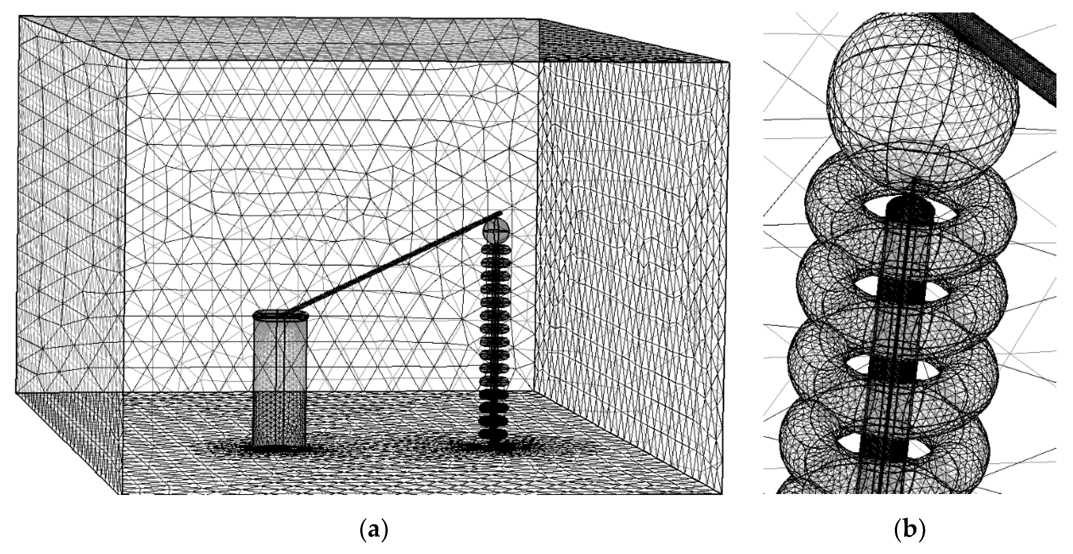
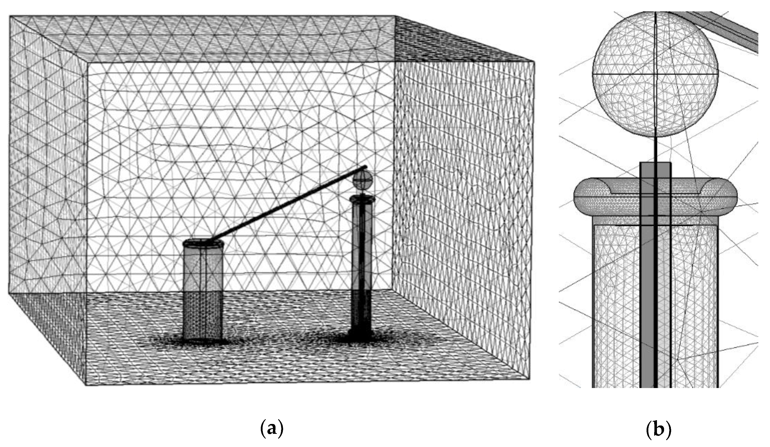
Section 4 develops the FEA model used to analyze the machine and validates this model by means of experimental data. Section 5 summarizes the experimental results, analyzes the effects of several parameters, including the size of the laboratory, and validates the performance of different corrective actions to minimize the effects of the stray capacitance. Finally, Section 6 condenses the conclusions of this paper.

2. Stray Capacitance Effects in Resistive High-Voltage Dividers and Circuital Model

Due to the increasing importance of high-voltage DC transmission systems, the development of accurate high-voltage DC measurement systems, which can be achieved with resistive dividers [19], is required. High-voltage dividers allow measuring the voltage between a high-voltage terminal and ground by reducing this value to an appropriate low-voltage on the low-voltage side of the divider. To this end, the transformation ratio must be known and must remain constant over a suitable frequency range. However, variables, such as frequency, temperature, or humidity, among others, can also affect the transformation ratio [20]. The main drawbacks of resistive dividers are related to power losses and stray capacitance, which often limit their use at voltages below 100 kV–50/60 Hz [21].
It is a recognized fact that resistive dividers offer good DC response, stability, and accuracy [19], although power dissipation, parasitic inductances, and capacitances can degrade the transient response and the accuracy of the measurements [22]. The high resistance of the voltage divider together with the stray capacitance to ground acts as a low-pass filter, whose cut-off frequency alters the frequency response of the divider [23]. Even so, the traditional design of precision high-voltage DC dividers is based on a resistive design, although they are only suitable for direct-current voltage measurements [24] if no appropriate shielding measures are applied.
The stray capacitance originates from the electric field lines directed from the divider to ground. Such lines can be contoured by using a big toroidal or circular-shaped shielding electrode placed at the high-voltage terminal, with a diameter comparable to the length of the divider, so for large dividers, this solution is unpractical. It is also possible to place different toroidal shielding electrodes at different heights along the high-voltage arm. The shielding electrodes force the electric field lines to follow the same direction throughout the whole divider, thus generating a quasi-uniform electric field distribution along the divider, thus minimizing the stray capacitance to ground [25].
The divider often requires a high-voltage grading electrode with suitable shape and dimensions to prevent the possibility of corona discharges. However, such electrode generates a capacitance to ground, which is often higher than the stray capacitance of the divider itself, thus affecting the voltage distribution along the resistors [26]. Stray capacitance appears between the divider and ground or between the divider and grounded objects. Therefore, the grounded objects and structural elements surrounding the measurement area can affect the stray capacitance and the precision of the measurement, thus altering the divider ratio [27]. The divider ratio in a DC voltage divider can be calculated as [24]
r = U 2 U 1 = R 2 n 1 · R 1 + R 2
n1 is the number of series-connected resistors R1 in the high-voltage arm of the resistor and R2 the resistance in the low-voltage arm, as shown in Figure 1a.
It is well-known that air is the dielectric that contributes most to stray capacitances [28]. In addition, practical resistors exhibit some amount of parasitic capacitance, since the metal leads or other parts have a certain ability to store charge.
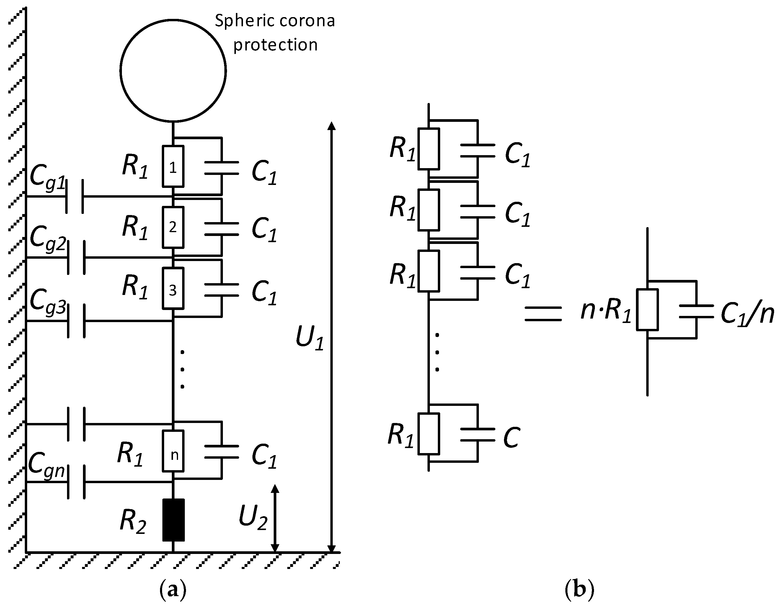
Figure 1 shows a circuit model of the divider, which includes the effects of the stray capacitances to ground and the parasitic capacitance of the resistors.
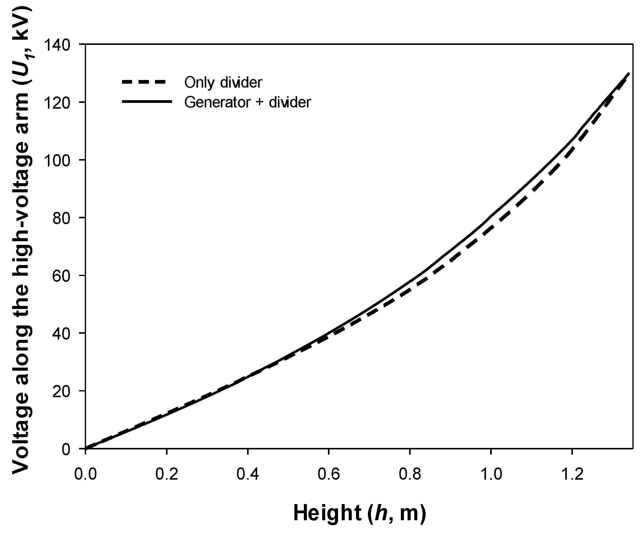
According to Figure 1a, due to the distributed stray capacitance to ground, the current through the top resistor is higher than the current through the bottom resistor, and thus, the voltage drop across the bottom resistor is lower than that across the top resistor (see Figure 7).
The exact calculation of the stray capacitance of the voltage divider is not simple since it depends on the exact location of the voltage divider with respect to all nearby conductor surfaces and objects [30]. However, according to [31], for a divider consisting of several sections, the stray capacitance to ground of each section can be calculated as [31]
C g = 2 π ε 0 l ln [ 2 l D ( 4 h + l 4 h + 3 l ) 1 / 2 ] = ( 55.6   pF / m ) l ln [ 2 l D ( 4 h + l 4 h + 3 l ) 1 / 2 ]
ε = 8.854 pF/m being the absolute permittivity of air, and l and D being, respectively, the length and diameter of each section of the metallic cylinder acting as a screen, which is supposed to be connected to the bottom of each section.
A similar formula to Equation (2) is found in [29]. These formulas are based on series-connected resistors enclosed in a metallic cylindrical shield. However, they present inherent limitations due to the assumptions that they are based on, and because they do not take into account several aspects, including the size of the laboratory, the distance to the grounded walls, floor and ceiling, or the influence of other metallic and grounded objects in the laboratory, such as the high-voltage generator or different measuring instruments which are already present in the laboratory.
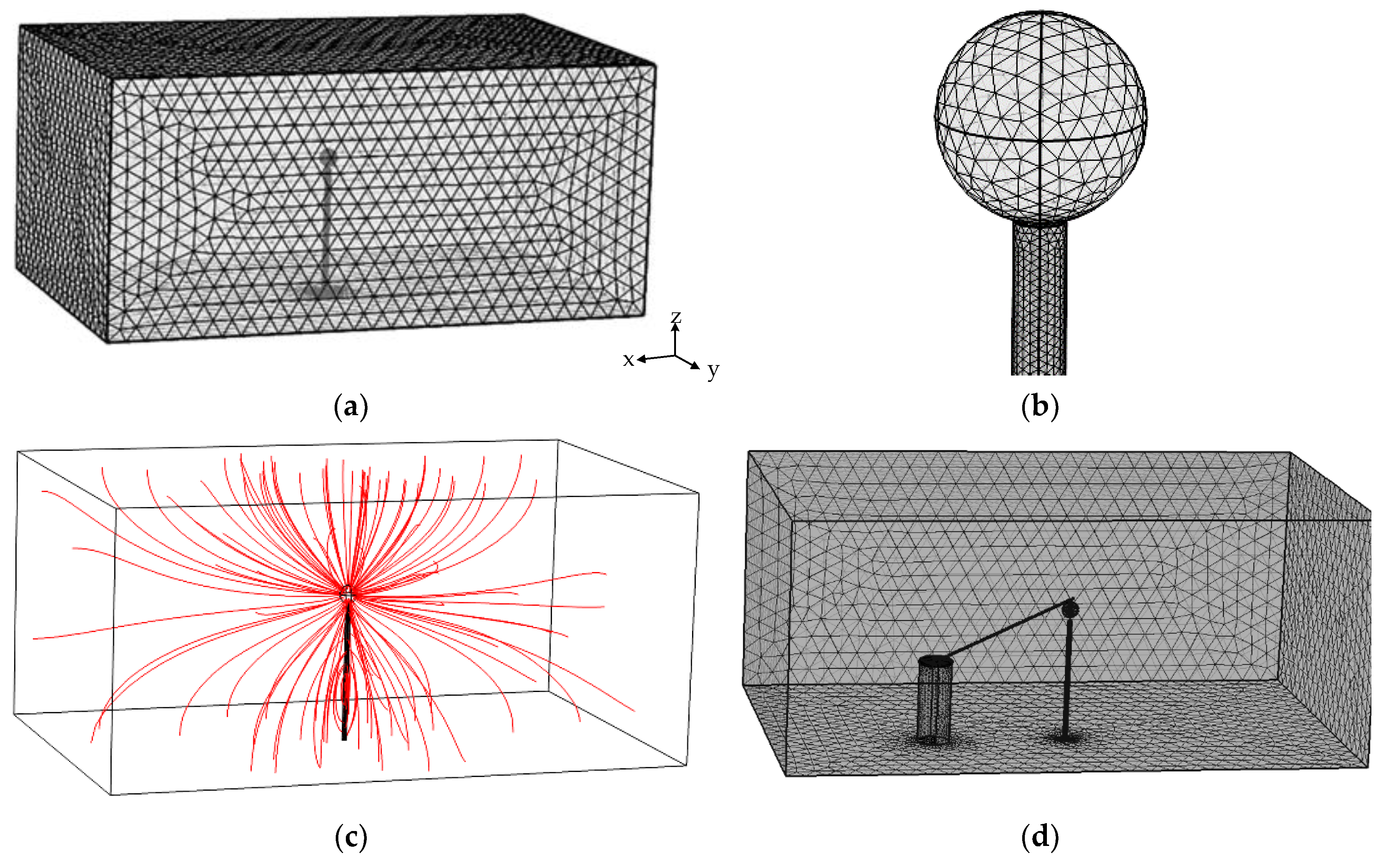
3. The Analyzed Resistive High-Voltage Divider

The resistive divider analyzed in this work comprises the high-voltage terminal, and the high-voltage and low-voltage arms, as shown in Figure 2. The high-voltage arm is composed of 60 non-inductive metal-oxide film-resistors [29] (Ohmite MOX-4-12, 40 MΩ each, 1%, <2 PPM/V, 25 PPM/°C, 0.30–0.75 pF) connected in series, whereas the low-voltage arm includes a low-ohmic resistor of 120 kΩ (metal film Welwyn/ TT Electronics PR5Y-120KBI, 1%, 25 PPM/°C). It results in a nominal voltage ratio of 1/20001, corresponding to 20.001 kV:1 V.

4. FEA Simulations to Determine the Effects of Stray Capacitance

The stray or parasitic capacitance to ground is closely related to the electric field distribution around the divider [25]. It can be calculated by using computer programs based on the charge distribution of the conductors [20], such as those based on FEA [12,23]. FEA models were developed using the Comsol Multiphysics® software package by conducting a frequency domain study at 50 Hz.

4.1. The FEA Formulation to Determine the Stray Capacitance

The effects of the parasitic or stray capacitance, are often unwanted and are especially notorious in high-voltage and high-frequency applications.
The capacitance is calculated by applying three steps. For low-frequency cases, it is enough to consider only the electrostatic field energy. First, the potential at the surface of the studied conductor is calculated, taking into account the quasi-static approximation, which disregards the displacement current. The next step consists of calculating the outer electric potential and the electric field in the points of the domain surrounding the high-voltage conducting body, by applying the known potential as the boundary condition [32,33]. To conclude, the capacitance of the system under analysis is computed from (8).
The Gauss law can be expressed as
· ( ε · E ) = ρ
E (V/m) being the electric field and ρ (C/m3) the charge density. Replacing E = · U in Equation (3), it results in Poisson’s equation for electrostatics [34].
2 U = ρ / ε
By solving Equation (4), the electric potential and the electric field in all points of the analyzed domain can be found [35]. Next, supposing the air as an isotropic medium, the energy density (J/m3) in the points of the domain is calculated.
u E ( x , y , z ) = 1 2 · ε o · E ( x , y , z ) 2
The stored electrostatic energy is obtained from the integral of the energy density over the volume of the analyzed domain.
W E = 1 2 v ε o · E ( x , y , z ) 2 d x d y d z
The energy stored within a capacitor is as follows:
W E = 1 2 · C · U 2
U (V) being the potential between the two terminals of the capacitor. Then, the capacitance between two terminals of the system can be calculated as in (8) [33].
C = 2 · W E / U 2
The capacitance is computed from the electric energy stored in the air due to the effect of U. When analyzing low-frequency applications, WE represents the energy stored in the electric field outside the conductive body [32].

4.2. FEA Application

The stray capacitance to ground Cg of the voltage divider has been simulated using the dimensions of the high-voltage laboratory of the UPC, which are 7.07 × 4.3 × 3.07 m3 (x, y, and z dimensions, respectively), as shown in Figure 3a, with the floor, walls, and ceiling at ground potential.
Figure 3 shows the mesh of the analyzed domains as well as streamline plots of the electric field lines around the divider and the generator, which provide information about the distributed capacitance between the high-voltage objects and the grounded elements of the laboratory.

5. Results

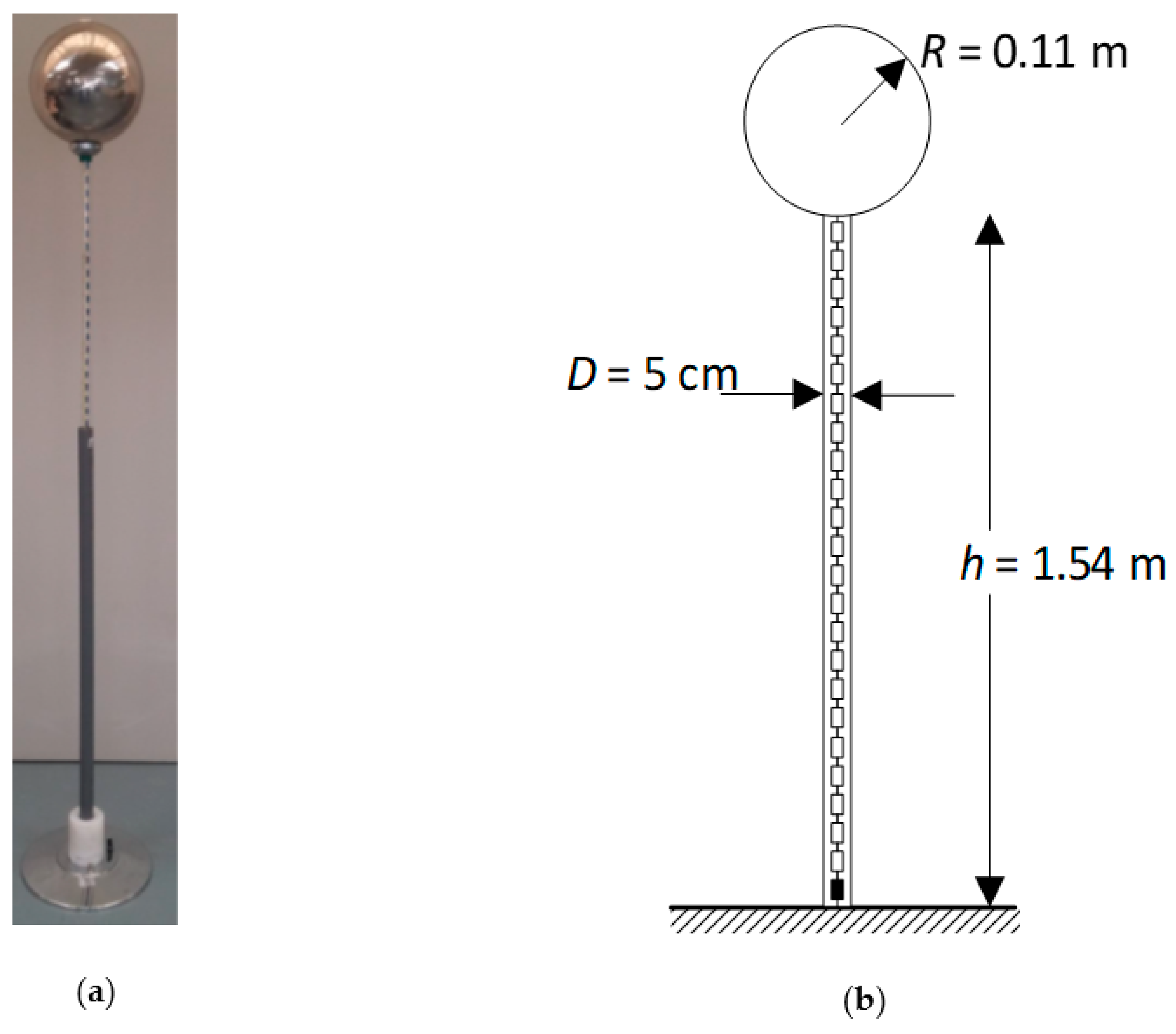
This section presents experimental and FEA results to study and evaluate stray capacitance effects. The capacitive effects are analyzed by analyzing the behavior of a 130 kV RMS high-voltage resistive divider under both AC and DC supply.
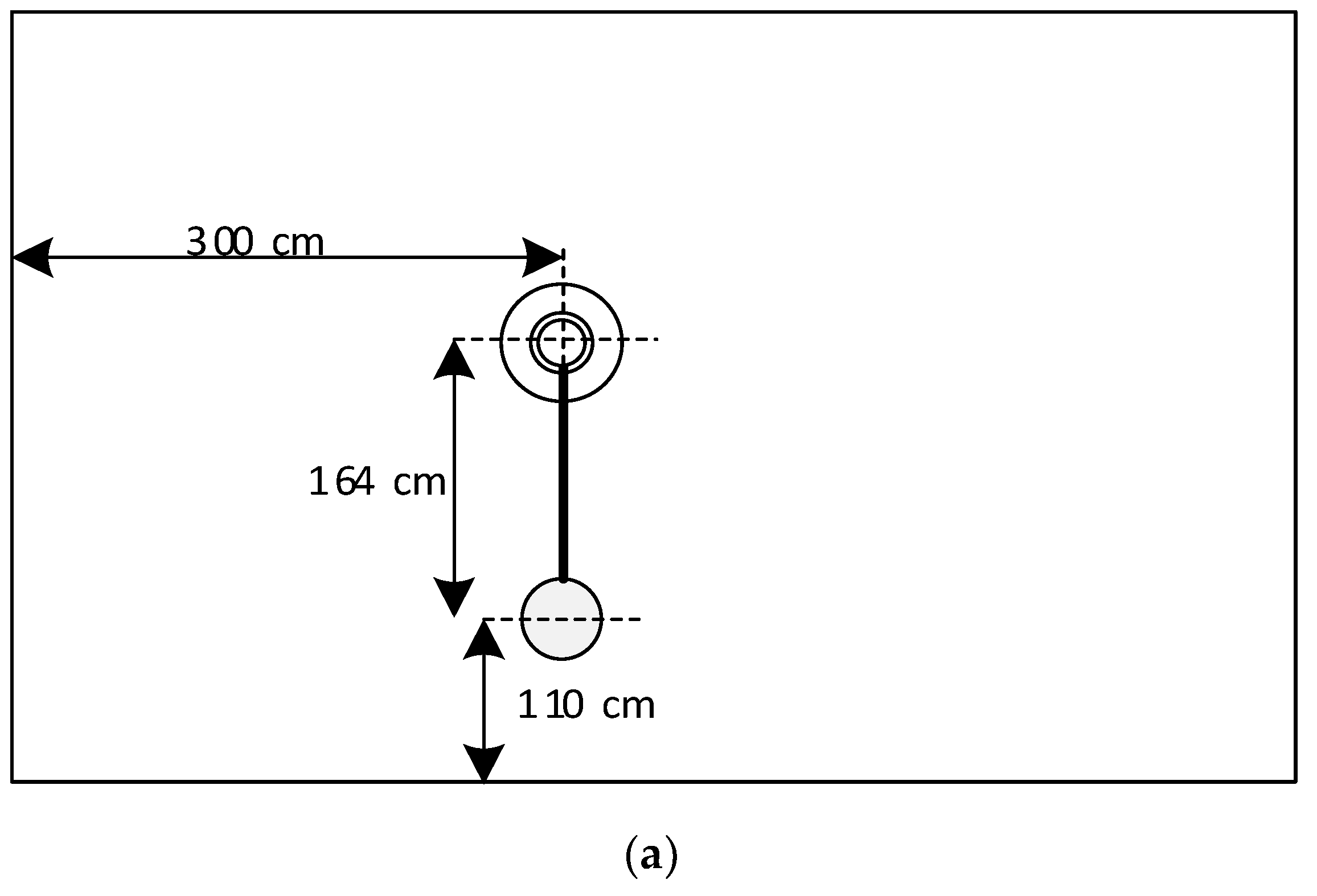
A DC high-voltage generator (PHENIX 4120-10, max. voltage + 120 kVDC), an AC voltage generator (PHENIX BK-130, max. voltage 130 kV RMS) and a Fluke 289 true RMS multi-meter were used to test the divider under DC and AC supply, respectively.
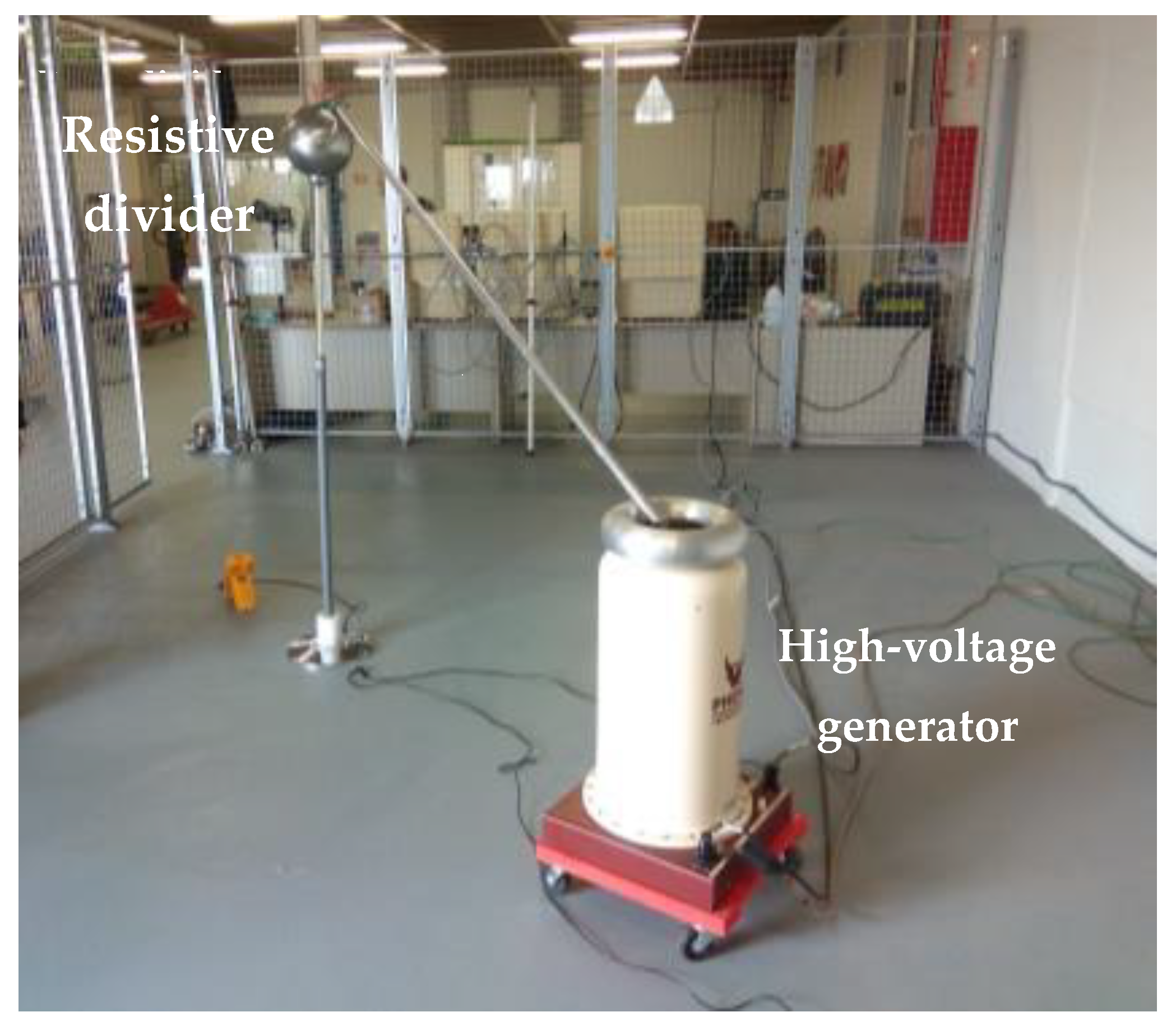
Figure 4 shows the AC high-voltage generator and the resistive divider inside the grounded laboratory.
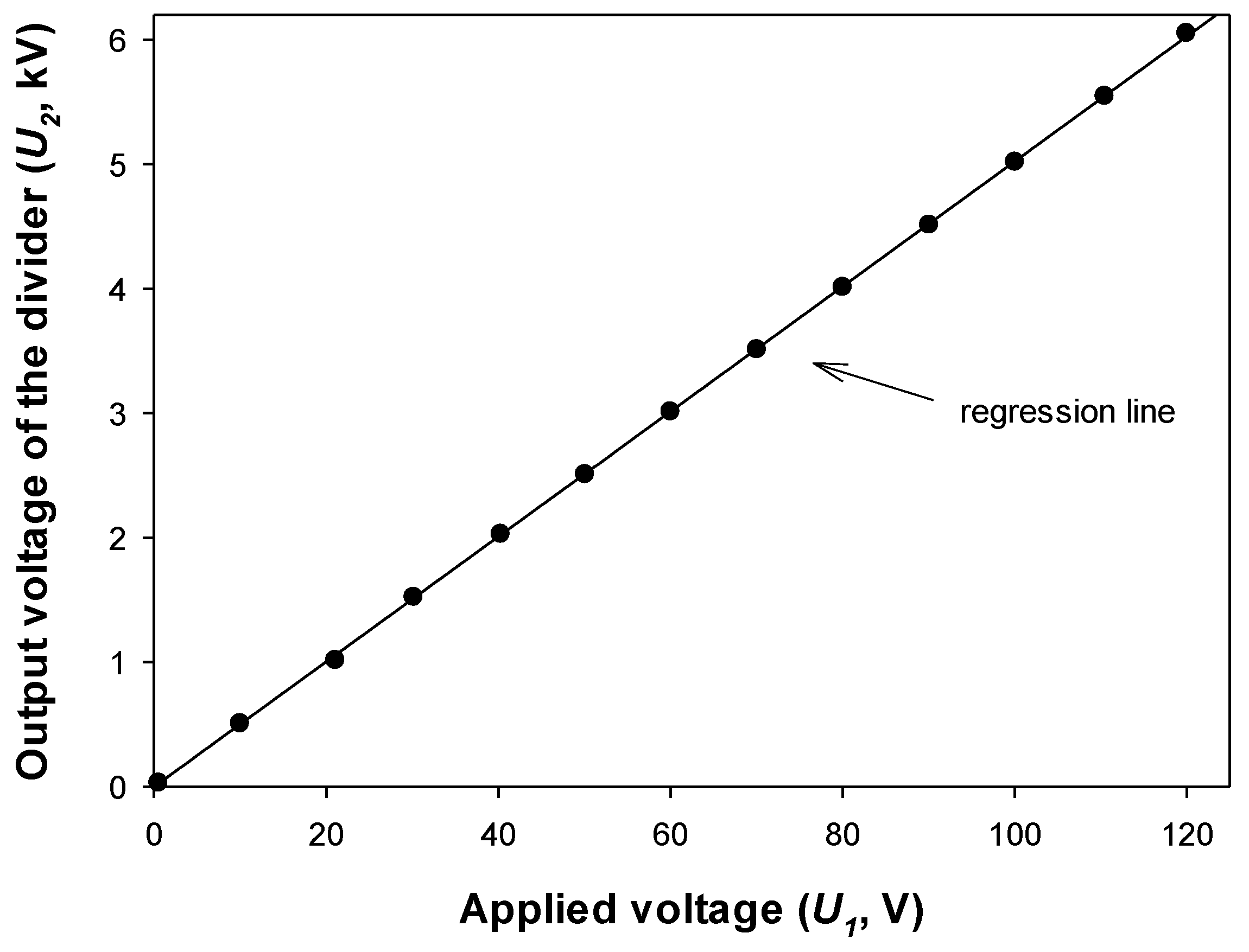
Figure 5 shows the experimental calibration made under positive DC supply using the 120 kV DC generator, which was carried out at the high-voltage laboratory of the Universitat Politècnica de Catalunya (UPC) under 12.2 °C, 58.0% RH and 976 hPa weather conditions.
Results presented in Figure 5 show that U1 and U2 follow a linear relationship given by U1 = 30.215 + 19,907.006·U2, with a coefficient of determination R2 = 0.999954. It is worth noting that the experimental slope of this straight line, corresponding to the voltage ratio, is almost 20,001, the nominal value, as expected. The difference (0.5%) lies within the 1% tolerance of the resistors used in the high-voltage divider.
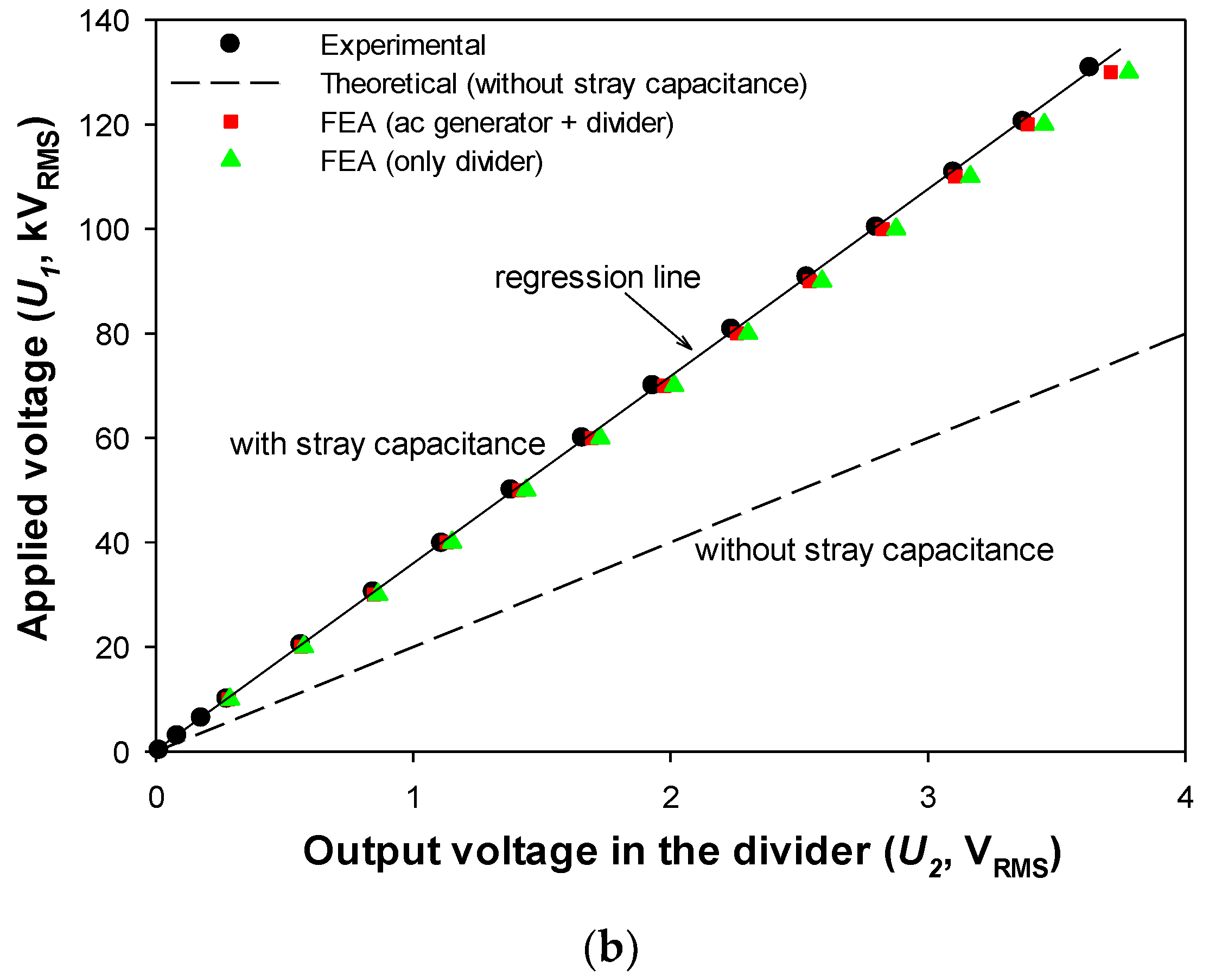
Figure 6 presents the experimental layout during the calibration carried out under AC supply using the 130 kV RMS AC generator. The atmospheric conditions during the test were 12.2 °C, 58.0% RH, and 976 hPa.
Results presented in Figure 6 show that U1 and U2 follow a linear relationship given by U1 = 130.947 + 35,877.873·U2, with a coefficient of determination R2 = 0.999937. The experimental slope of this straight line (35,877.873) is far from the nominal value of 20,001, due to the effects of the stray capacitance, thus severely affecting the divider ratio and the accuracy of the voltage divider. Therefore, when applying 130 kV RMS and assuming the layout shown in Figure 6a, the output voltage of the low-voltage arm of the divider is 3.62 V RMS instead of the theoretical value of 6.50 V RMS.
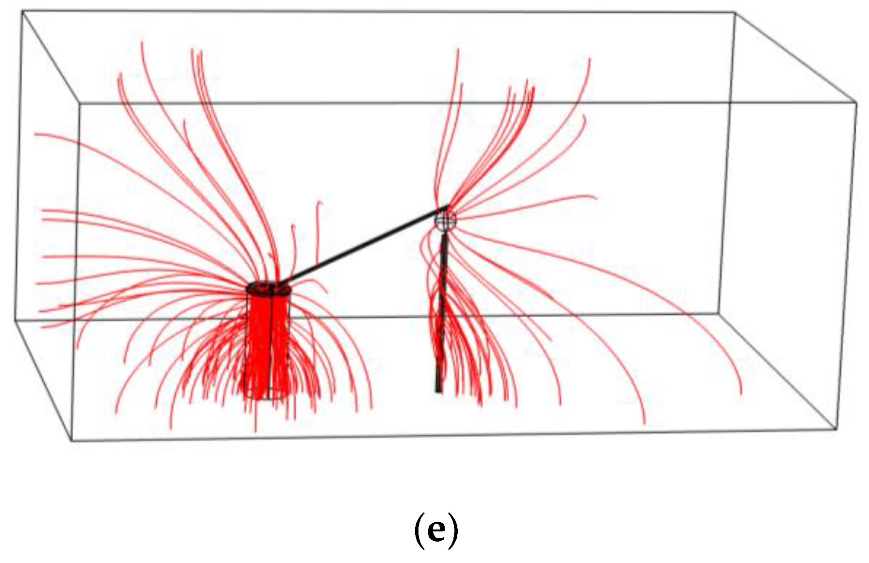
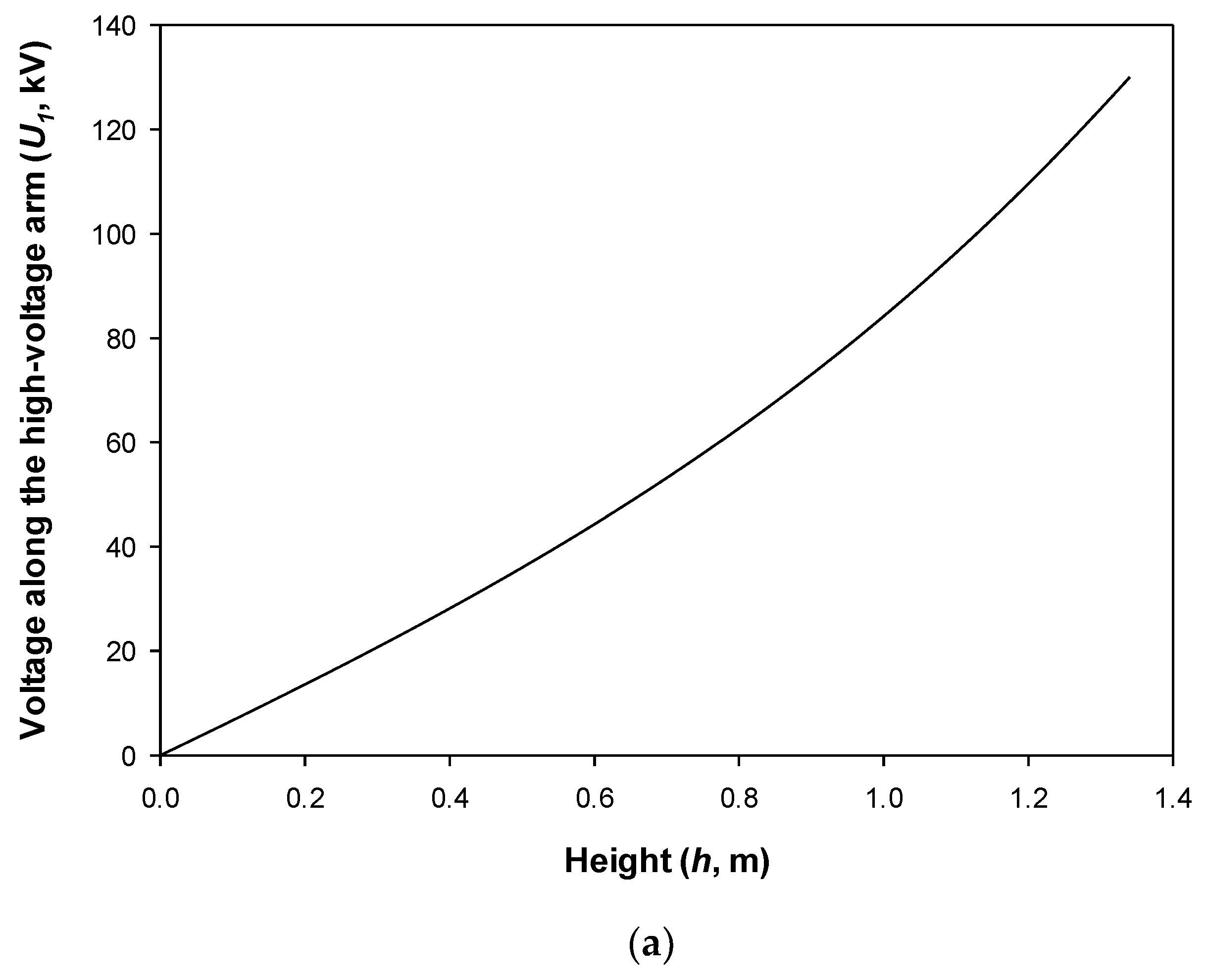
Figure 7 shows the uneven voltage distribution along the length of the high-voltage arm of the resistive divider, obtained by means of FEA simulations. Due to the distributed stray capacitance to ground, the current through the upper resistors of the high-voltage arm of the divider is higher than that through the lower resistors. Therefore, the voltage drop in the resistors farthest from the ground is greater than in those closest to the ground. This effect depends on the geometry of the high-voltage arrangement.
Although a guard electrode configuration can be used to minimize the impact of the stray capacitance on the measured voltage U2 [31,36], this configuration has not been used in the results above to stress the effect of the stray capacitance.

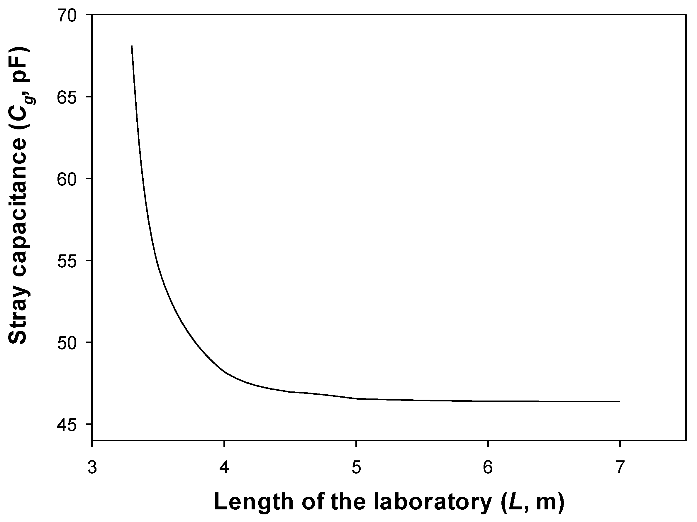
5.1. The Effect of the Laboratory Dimensions

According to (6) and (7), the stored electrostatic energy and thus, the capacitance, is influenced by the size of the laboratory.
In this section, this influence is investigated by means of FEA simulations, by changing the length of the laboratory from 3.3 m to 7 m. The results attained are summarized in Figure 8.
Results presented in Figure 8 clearly show that the stray capacitance Cg decreases when increasing the size of the laboratory; its value tending to stabilize when the size of the laboratory is beyond a determined value

5.2. Evaluation of Possible Corrective Strategies

As already explained, the large dimensions of high-voltage dividers generate distributed stray capacitances between the divider and high-voltage electrodes to ground. Several solutions can be applied to eliminate or minimize the impact of stray capacitance in high-voltage resistive dividers, including metal screens (grounded concentric electrodes) [28] or guard electrode configurations [31,36]. Another option is to use capacitive dividers for alternating current tests and switching impulse tests or damped capacitive dividers for switching impulse and lightning impulse tests [31].
Due to the stray capacitance, the dynamic behavior of the divider can change, the rate of change being affected by the frequency of the test voltage. This is an issue in applications involving fast, impulse signals, which are composed of a wide spectral range, in which the dynamic response of voltage dividers can be significantly affected [28].
Therefore, a solution to lessen the effects of stray capacitance is highly appealing, especially cases requiring the use of DC dividers for AC measurements, since high-voltage dividers are expensive devices.

5.2.1. Using Grading Rings to Minimize the Stray Capacitance

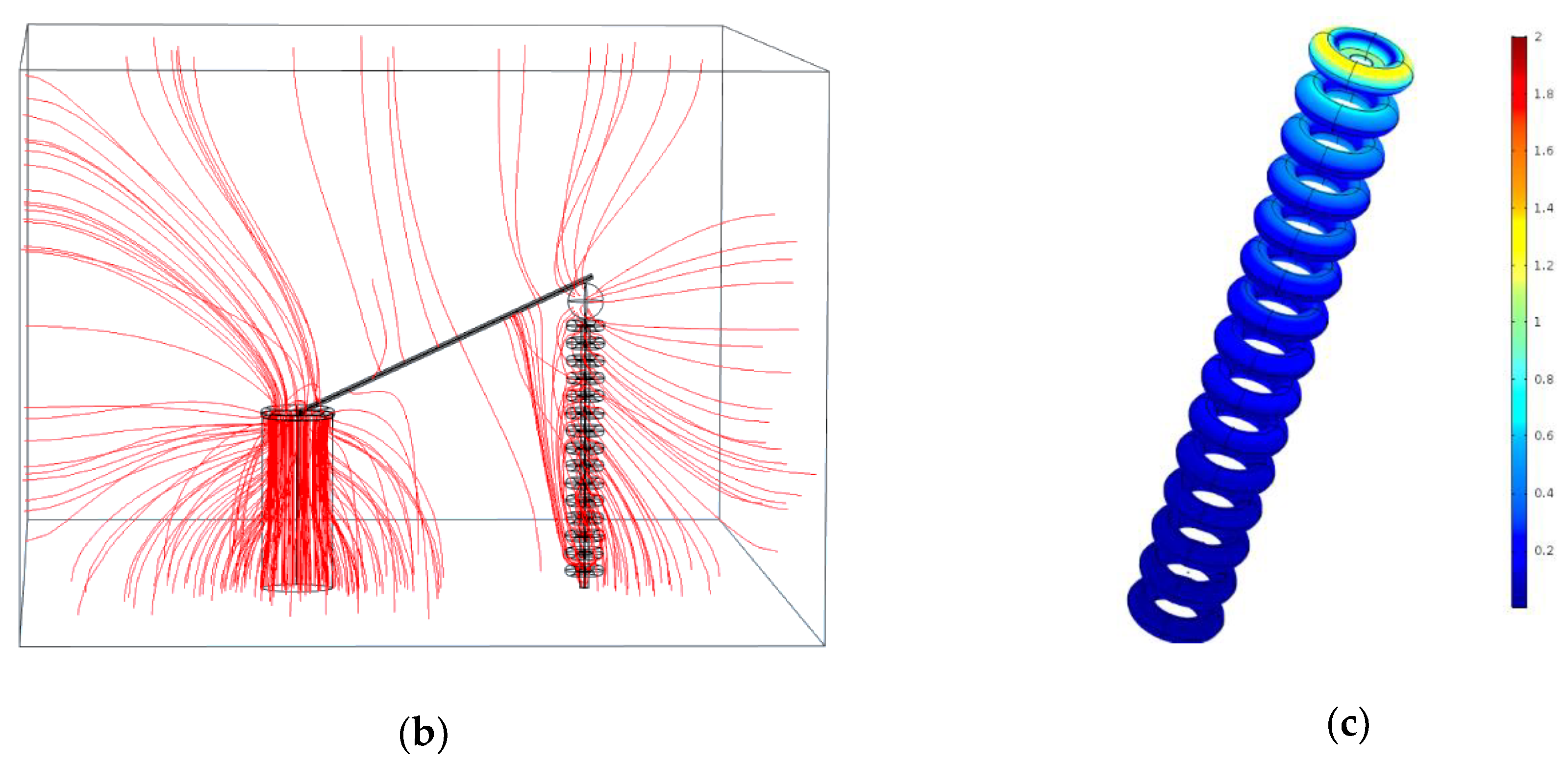
One possibility found in the technical literature is to use grading rings to limit the stray capacitance effect. To prove the performance of the addition of the grading rings, 15 aluminum grading rings equally spaced were added to the high-voltage divider, as shown in Figure 9. The inner and outer radiuses of the rings are 30 and 80 mm, respectively.
Figure 10 shows that despite using a row of 15 aluminum grading rings, the voltage distribution along the high-voltage arm of the resistive divider is still not linear due to the effects of the remaining stray capacitance not blocked by the rings.
The stray capacitance obtained according to the geometry proposed in Figure 10 is Cg = 46.54 pF, and the output voltage of the high-voltage resistive divider at 130 kV RMS is 4.42 V RMS, which is still far from the theoretical value of 6.50 V RMS, thus resulting in an error around 32.0%. This is because there are still many electric field lines departing from the divider arms to ground, as shown in Figure 10b. Figure 10c displays the electric field strength on the surface of the grading rings, thus proving that there is no corona effect on the outer surface of the grading rings inception.

5.2.2. Using a Grading Hollow Cylinder to Minimize the Stray Capacitance

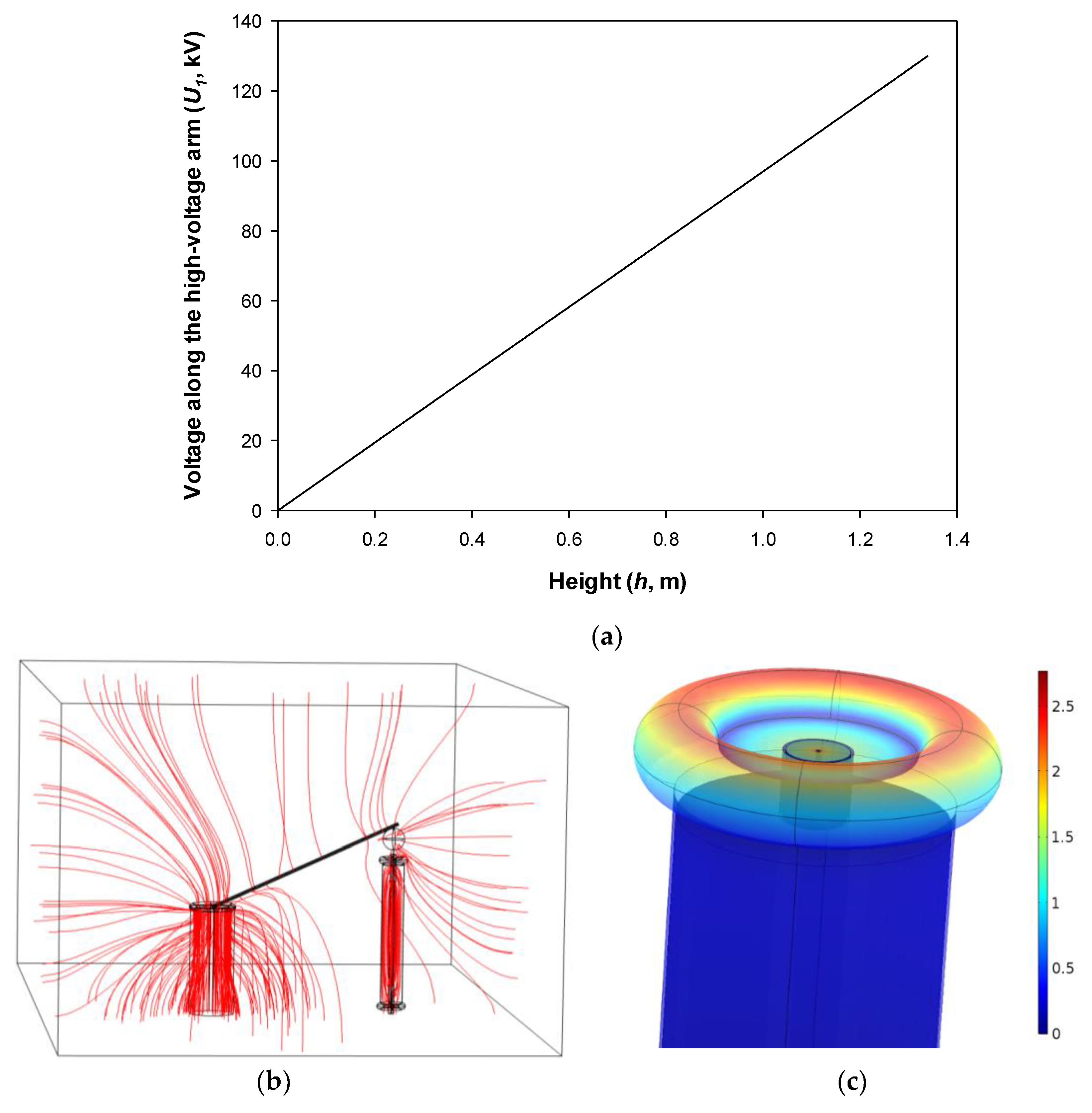
Another possible solution to limit the effects of stray capacitance in resistive high-voltage dividers is the use of a grading hollow cylinder, which acts as a Faraday cage for the electric field lines departing from the arms of the divider. This solution is shown in Figure 11.
Figure 12 shows that when using an aluminum grading hollow cylinder, the voltage distribution along the high-voltage arm of the resistive divider is very linear, thus verifying the excellent performance of such a solution. This is because the electric field lines departing from the divider arms are self-contained inside the inner volume of the grading hollow cylinder, as shown in Figure 12b. Figure 12c displays the distribution of the electric field strength on the surface of the hollow cylinder, whose values are below the corona inception threshold.
The stray capacitance obtained according to the geometry proposed in Figure 11 is Cg = 6.28 × 10⁻³ pF, this being a very low value that proves the usefulness of this solution. In addition, the output voltage of the high-voltage resistive divider when applying 130 kV RMS is 6.53 V RMS, which is very close to the theoretical value of 6.50 V RMS, resulting in an error around 0.5%, below the tolerance of the resistors of the divider. This reduced stray capacitance allows improving the dynamic response of the divider since it depends on the RCg product.
The results presented in this section clearly show that the use of an array of grading rings is not the most suitable alternative, since stray capacitance effect is only partially removed, and a certain free space around the divider must be left, where no objects can be placed. The dimensions of this area depend on the geometry of the divider and the rings and must be either identified by means of direct experimentation or calculated.
Instead, a grading hollow cylinder is a cost-effective solution that allows minimizing the effects of stray capacitance, and thus, when well designed, it almost removes all capacitive effects. In addition, the region around the divider has less influence.

6. Conclusions

This paper has analyzed the effect of the distributed stray capacitance to ground in the accuracy of resistive high-voltage dividers operating under DC and AC supply by means of experimental data and three-dimensional FEA simulations. It has been shown that FEA simulations allow calculating both the stray capacitance and the distortion in the output voltage of the divider, thus allowing the quantification of their effects. The work has also analyzed the impact of several parameters on the accuracy of the resistive high-voltage divider, including the size of the laboratory and two types of grading electrodes added to the body of the resistive divider to mitigate the effects of the stray capacitance, namely toroidal grading rings and a grading hollow cylinder. It has been shown that, whereas the addition of toroidal grading rings provides only a partial correction and thereby, partial improvement in the behavior of the resistive divider, the addition of a grading hollow cylinder performs much better, being an excellent solution, which allows improving the dynamic response of the divider. The results and data shown in this work can be used as a reference for determining the effects of stray capacitance in high-voltage dividers, thus allowing the design of corrective actions in resistive high-voltage dividers for AC measurements.

Author Contributions

J.-R.R. conceived and designed the numerical tests, performed the experimental tests, analyzed the data, and wrote the paper; M.M.-E. performed the experimental tests and analyzed the data; F.C. performed the simulations.

Funding

This research was funded in part by the Generalitat de Catalunya under Project 2017 SGR 967 and in part by the Spanish Ministry of Economy and Competitiveness under Project RTC-2017-6297-3.

Conflicts of Interest

The authors declare no conflict of interest.

References

  1. Maruvada, P.S.; Hylten-Cavallius, N. Capacitance calculations for some basic high voltage electrode configurations. IEEE Trans. Power Appar. Syst. 1975, 94, 1708–1713. [Google Scholar] [CrossRef]
  2. Capelli, F.; Riba, J.-R.R. Analysis of formulas to calculate the AC inductance of different configurations of nonmagnetic circular conductors. Electr. Eng. 2017, 99, 827–837. [Google Scholar] [CrossRef]
  3. Riba, J.-R.; Capelli, F. Analysis of capacitance to ground formulas for different high-voltage electrodes. Energies 2018, 11, 1090. [Google Scholar] [CrossRef]
  4. Iossel, Y.Y.; Kochanov, E.S.; Strunskiy, M.G. The Calculation of Electrical Capacitance; DTIC: Springfield, VA, USA, 1969. [Google Scholar]
  5. Ganuza, D.; García, F.; Zulaika, M.; Perez, A.; Jones, T.T.C. 130 kV 130 A high voltage switching mode power supply for neutral beam injectors—Control issues and algorithms. Fusion Eng. Des. 2005, 75–79, 253–258. [Google Scholar] [CrossRef]
  6. Tonmitr, N.; Tonmitr, K.; Kaneko, E. The Effect of Controlling Stray and Disc Capacitance of Ceramic String Insulator in the Case of Clean and Contaminated Conditions. Procedia Comput. Sci. 2016, 86, 333–336. [Google Scholar] [CrossRef] [Green Version]
  7. Ilhan, S.; Ozdemir, A. Voltage Distribution Effects of Non-Uniform Units in Suspension Strings. In Proceedings of the 2007 IEEE Lausanne Power Tech, Lausanne, Switzerland, 1–5 July 2007; pp. 801–806. [Google Scholar]
  8. Wu, C.; Cheng, T.; Rodriguez-Pena, A. A Study on the Use of Internal Grading to Improve the Performance of Insulators. IEEE Trans. Electr. Insul. 1981, EI-16, 250–257. [Google Scholar] [CrossRef]
  9. Kontargyri, V.T.; Gonos, I.F.; Stathopulos, I.A. Measurement and simulation of the electric field of high voltage suspension insulators. Eur. Trans. Electr. Power 2009, 19, 509–517. [Google Scholar] [CrossRef]
  10. Heylen, A.E.D.; Hartles, S.E.; Noltsis, A.; Dring, D. Low and High Voltage Distribution Along a Cap and Pin Insulator String Subjected to AC and Impulse Voltages. In Gaseous Dielectrics VI; Springer: Boston, MA, USA, 1991; pp. 267–272. [Google Scholar]
  11. Dalessandro, L.; da Silveira Cavalcante, F.; Kolar, J.W. Self-Capacitance of High-Voltage Transformers. IEEE Trans. Power Electron. 2007, 22, 2081–2092. [Google Scholar] [CrossRef]
  12. Song, J.K.; Lv, D.; Zhang, H.H. The Modeling and Magnetic Simulation of Resistance High-Voltage Divider Based on AutoCAD and Maxwell. Appl. Mech. Mater. 2013, 307, 231–235. [Google Scholar] [CrossRef]
  13. Permata, D.; Nagaoka, N. Modeling method of fast transient for unsymmetrical stray capacitance to ground. IEEJ Trans. Electr. Electron. Eng. 2015, 10, S28–S33. [Google Scholar] [CrossRef]
  14. Dolinko, A.E. Kirchhoff and Ohm in action: Solving electric currents in continuous extended media. Eur. J. Phys. 2018, 39, 025201. [Google Scholar] [CrossRef]
  15. Girwidz, R. V Visualizing dipole radiation. Eur. J. Phys. 2016, 37, 065206. [Google Scholar] [CrossRef]
  16. Riba, J.-R. Calculation of the ac to dc resistance ratio of conductive nonmagnetic straight conductors by applying FEM simulations. Eur. J. Phys. 2015, 36, 1–10. [Google Scholar] [CrossRef]
  17. Yang, J.; Zhang, W.; Zou, L.; Wang, Y.; Sun, Y.; Feng, Y.; Yang, J.; Zhang, W.; Zou, L.; Wang, Y.; et al. Research on Distribution and Shielding of Spatial Magnetic Field of a DC Air Core Smoothing Reactor. Energies 2019, 12, 937. [Google Scholar] [CrossRef]
  18. Alharbi, H.; Khalid, M.; Abido, M.; Alharbi, H.; Khalid, M.; Abido, M. A Novel Design of Static Electrostatic Generator for High Voltage Low Power Applications Based on Electric Field Manipulation by Area Geometric Difference. Energies 2019, 12, 802. [Google Scholar] [CrossRef]
  19. Li, Y.; Ediriweera, M.K.; Emms, F.S.; Lohrasby, A. Development of Precision DC High-Voltage Dividers. IEEE Trans. Instrum. Meas. 2011, 60, 2211–2216. [Google Scholar] [CrossRef]
  20. Kaane, H.L. Calculation of the response time of shielded high voltage resistive dividers. Eur. Trans. Electr. Power 2007, 1, 73–77. [Google Scholar] [CrossRef]
  21. Abdel-Salam, M. High-Voltage Engineering: Theory and Practice; CRC Press: Boca Raton, FL, USA, 2000. [Google Scholar]
  22. Boggs, S.A.; FitzPatrick, G.J.; Kuang, J. Transient errors in a precision resistive divider. In Proceedings of the Conference Record of the 1996 IEEE International Symposium on Electrical Insulation, Montreal, QC, Canada, 16–19 June 1996; Volume 2, pp. 482–485. [Google Scholar]
  23. Klüss, J.; Hällström, J.; Elg, A.-P. Optimization of field grading for a 1000 KV wide-band voltage divider. J. Electrostat. 2015, 73, 140–150. [Google Scholar] [CrossRef]
  24. Küchler, A. High Voltage Engineering Fundamentals—Technology—Applications; Springer: Berlin/Heidelberg, Gremany, 2018. [Google Scholar]
  25. Naidu, S.R.; Neto, A.F.C. The Stray-Capacitance Equivalent Circuit for Resistive Voltage Dividers. IEEE Trans. Instrum. Meas. 1985, IM-34, 393–398. [Google Scholar] [CrossRef]
  26. Rizk, F.A.M.; Trinh, G.N. High Voltage Engineering; CRC Pr I LLC: Boca Raton, FL, USA, 2017. [Google Scholar]
  27. Yang, C.; Wu, M.; Jian, C.; Yu, J. The stray capacitance on precision of high-voltage measurement. In Proceedings of the 2009 IEEE Intrumentation and Measurement Technology Conference, Singapore, 5–7 May 2009; pp. 249–253. [Google Scholar]
  28. Arora, R.; Mosch, W. High Voltage and Electrical Insulation Engineering; John Wiley & Sons: Hoboken, NJ, USA, 2011. [Google Scholar]
  29. Kuffel, J.; Zaengl, W.S.; Kuffel, P. High Voltage Engineering Fundamentals, 2nd ed.; Newnes: Oxford, UK, 2000. [Google Scholar]
  30. Hermach, F.L.; Dziuba, R.F. Precision Measurement and Calibration. Electricity—Low Frequency—Google Libros; Astin, A.V., Ed.; National Bureau of Standards, United States Department of Commerce: Washington, DC, USA, 1968.
  31. Hauschild, W.; Lemke, E. High-Voltage Test and Measuring Techniques; Springer: New York, NY, USA, 2014. [Google Scholar]
  32. Yu, Q.; Holmes, T.W. A study on stray capacitance modeling of inductors by using the finite element method. IEEE Trans. Electromagn. Compat. 2001, 43, 88–93. [Google Scholar]
  33. Chen, Y.; Yuan, J.S. Calculation of Single Conductor Capacitance by Estimating the Electrostatic Field. Adv. Mater. Res. 2012, 542–543, 1242–1247. [Google Scholar] [CrossRef]
  34. Hernández-Guiteras, J.; Riba, J.-R.; Romeral, L. Redesign process of a 765 kVRMS AC substation connector by means of 3D-FEM simulations. Simul. Model. Pract. Theory 2014, 42, 1–11. [Google Scholar] [CrossRef]
  35. Riba, J.-R.; Abomailek, C.; Casals-Torrens, P.; Capelli, F. Simplification and cost reduction of visual corona tests. IET Gener. Transm. Distrib. 2018, 12, 834–841. [Google Scholar] [CrossRef] [Green Version]
  36. Seanor, D.A. Electrical Properties of Polymers; Academic Press: Cambridge, MA, USA, 1982. [Google Scholar]
Figure 1. (a) Circuital model of the resistive divider, including the distributed stray capacitances Cgi between the divider and ground, (b) Equivalent circuit of the resistors including the effect of their own capacitance C1, (c) Equivalent circuit (circuital model) with concentrated stray capacitances to ground of a network of series-connected resistors, where theoretically k = 0.67 for equal response times, and k = 0.44 for equal bandwidth when enclosed in a metallic cylindrical shield [24,29].
Energies 12 02278 g001aEnergies 12 02278 g001b
Figure 2. (a) High-voltage resistive divider analyzed in this work, (b) Main dimensions of the resistive divider.
Energies 12 02278 g002
Figure 3. (a) Mesh of the entire domain of the resistive divider. (b) Mesh in the surface of the divider. (c) Streamline plot of the electric field lines around the divider within the analyzed domain. (d) Mesh of the entire domain, including the AC generator. (e) Streamline plot of the electric field lines around the divider and the generator.
Energies 12 02278 g003aEnergies 12 02278 g003b
Figure 4. High-voltage resistive divider analyzed in this work and AC generator.
Energies 12 02278 g004
Figure 5. Response of the resistive divider under positive DC supply. Experimental points.
Energies 12 02278 g005
Figure 6. Behavior of the resistive divider under power frequency AC supply (50 Hz). (a) Layout showing the divider and the AC generator (not in scale), (b) Experimental points and finite element analysis (FEA) simulations considering the AC generator (it results in Cg = 47.07 pF, k = 0.16) and without the generator (only the divider, Cg = 12.98 pF, k = 0.58).
Energies 12 02278 g006aEnergies 12 02278 g006b
Figure 7. Uneven voltage distribution along the high-voltage arm of the divider considering full assembly (including the AC generator and divider) and only considering the divider.
Energies 12 02278 g007
Figure 8. Effects of the length of the laboratory on the stray capacitance Cg calculated by means of a parametric FEA simulation. The dimensions of the laboratory are (7.07 m, [3.3–7.0] m, 3.07 m) in the (x,y,z) axes, respectively.
Energies 12 02278 g008
Figure 9. Grading rings added to the resistive high-voltage divider to minimize the effects of the stray capacitance. (a) Mesh of the full layout, including the high-voltage source, the divide, and the grading rings, (b) Detail of the aluminum grading rings.
Energies 12 02278 g009
Figure 10. Grading rings added to the resistive high-voltage divider to minimize the effects of the stray capacitance. (a) Voltage distribution along the high-voltage arm of the divider, (b) Streamline plot of the electric field lines around the divider, (c) Electric field strength on the surface of the cylindrical protection at 130 kV RMS.
Energies 12 02278 g010aEnergies 12 02278 g010b
Figure 11. Vertical grading cylinder (aluminum, R = 0.1 m) with a top corona protection toroid to minimize the effects of the stray capacitance. (a) Mesh of the full layout, including the high-voltage source, the divider, and the grading cylinder, (b) Detail of the aluminum grading cylinder.
Energies 12 02278 g011
Figure 12. Grading hollow cylinder added to the resistive high-voltage divider to minimize the effects of the stray capacitance. (a) Voltage distribution along the high-voltage arm of the divider, (b) Streamline plot of the electric field lines around the divider, (c) Electric field strength on the surface of the cylindrical protection at 130 kV RMS.
Energies 12 02278 g012

