Interleaved High Step-Up DC-DC Converter Based on Voltage Multiplier Cell and Voltage-Stacking Techniques for Renewable Energy Applications †


Abstract
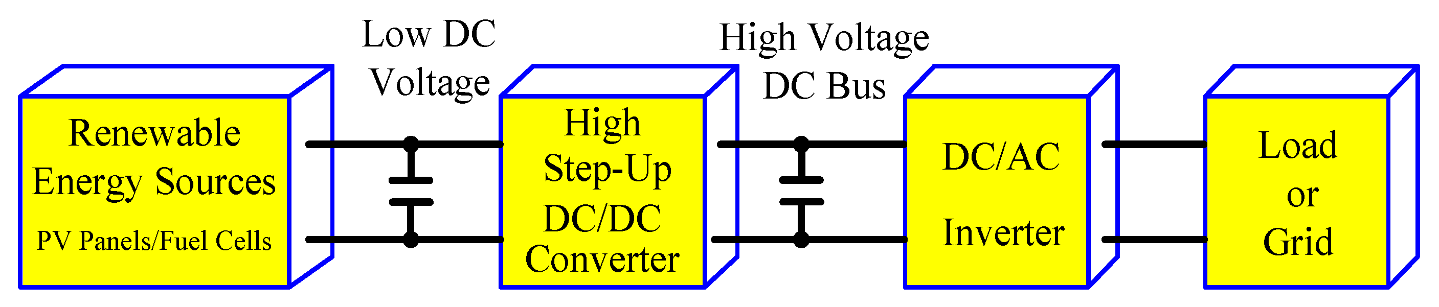
:1. Introduction
- (1)
- The converter has high step-up voltage gain without operating at extreme large duty ratio.
- (2)
- The voltage stress on the power switches is significantly lower than the output voltage. The low-voltage-rated MOSFETs with low on-resistances can thereby be adopted to reduce the conduction losses.
- (3)
- The diode reverse-recovery problem can be alleviated by the leakage inductances of the coupled inductors for most of the diodes.
- (4)
- Dual passive clamp circuits help to recycle the leakage energy of the coupled inductors and clamp the voltage stress of the power switches to a lower level.
- (5)
- The input current ripple, reduces is minimized due to the current ripple cancellation in the interleaved operation. Additionally, increases power level can be increased due to the current-sharing performance in high current applications.
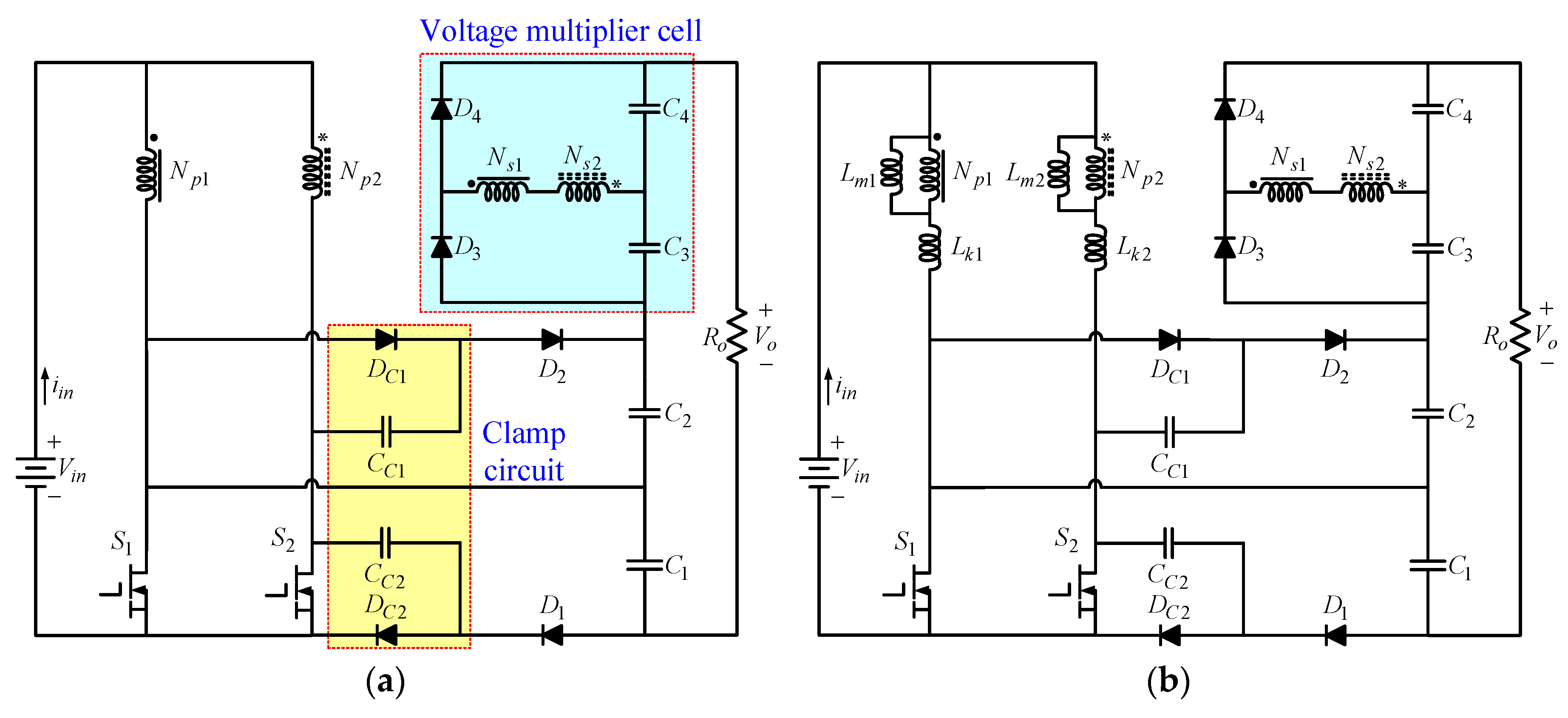
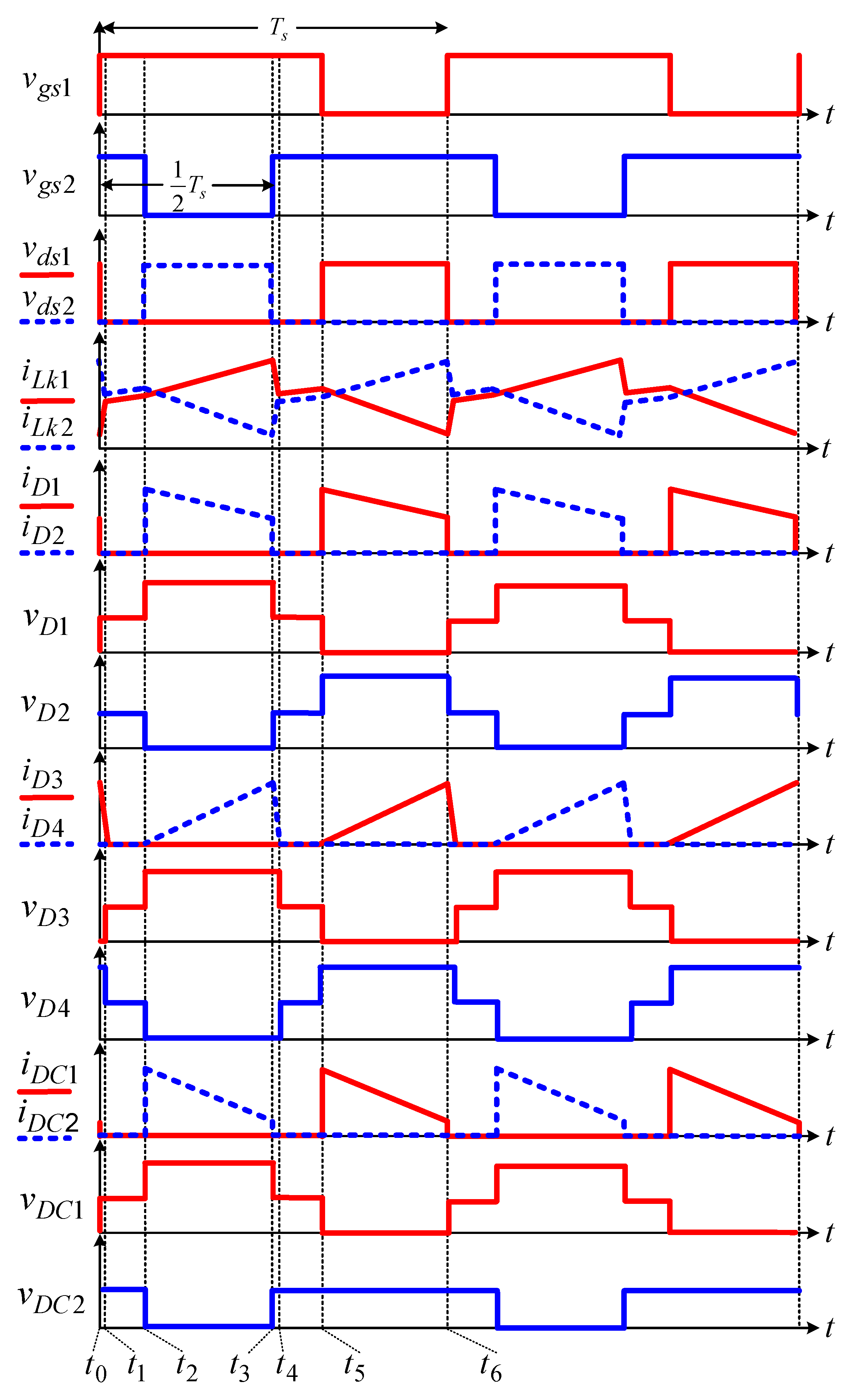
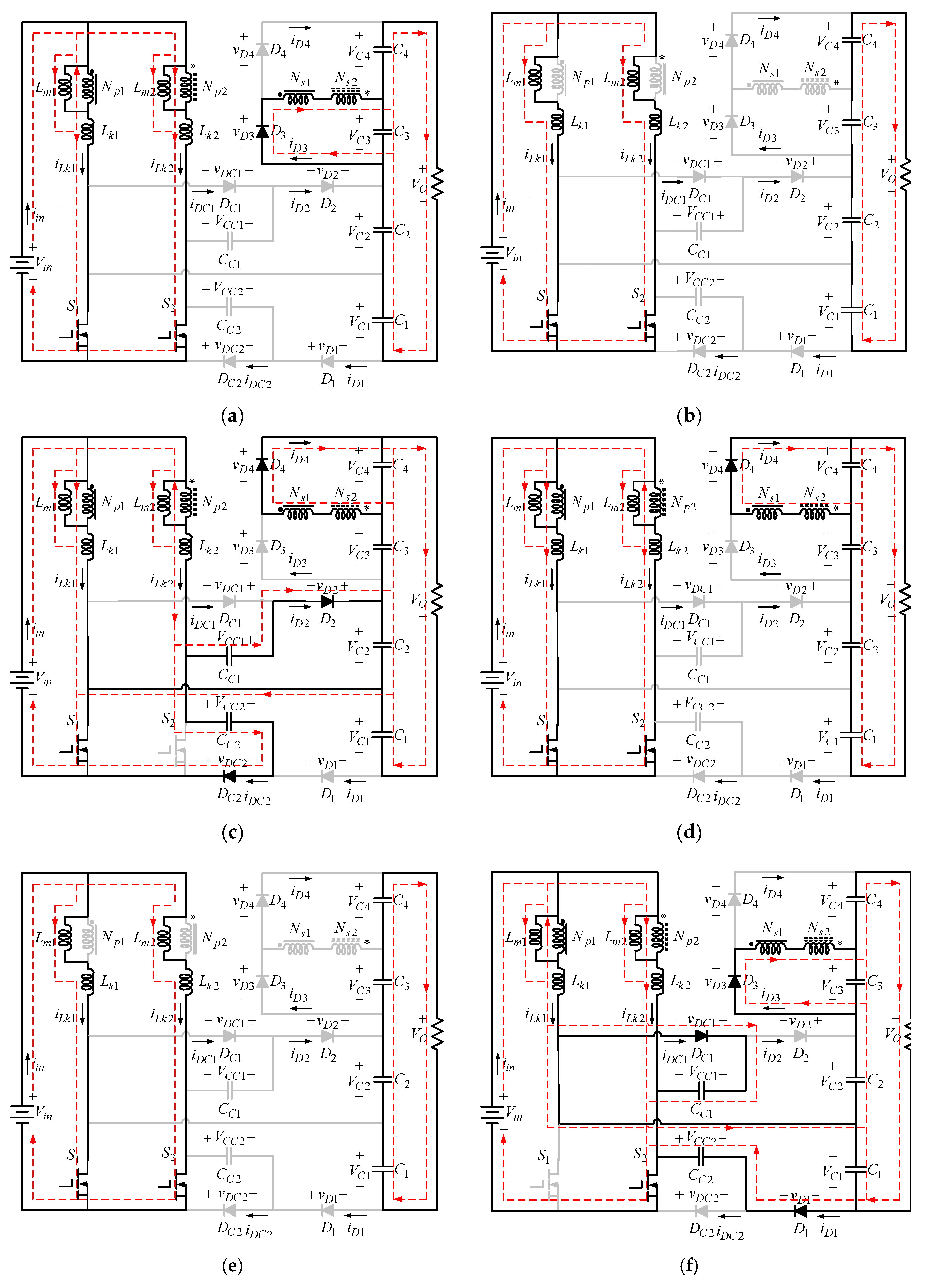
2. Proposed Converter and Operating Principle
3. Steady-State Analysis and Design Guidelines
- (1)
- Voltages on the capacitors are regarded as constant over one switching period due to their sufficiently large capacitances.
- (2)
- All of the power devices are ideal. The on-resistance and parasitic capacitances of the power switches are ignored, and the forward voltage drops of the diodes are neglected.
- (3)
- The leakage inductances of the couple inductors are much smaller than the magnetizing inductances, and, therefore, they are neglected.
- (4)
- The switching period is . The power switches operate with the same duty ratio D and out of phase.
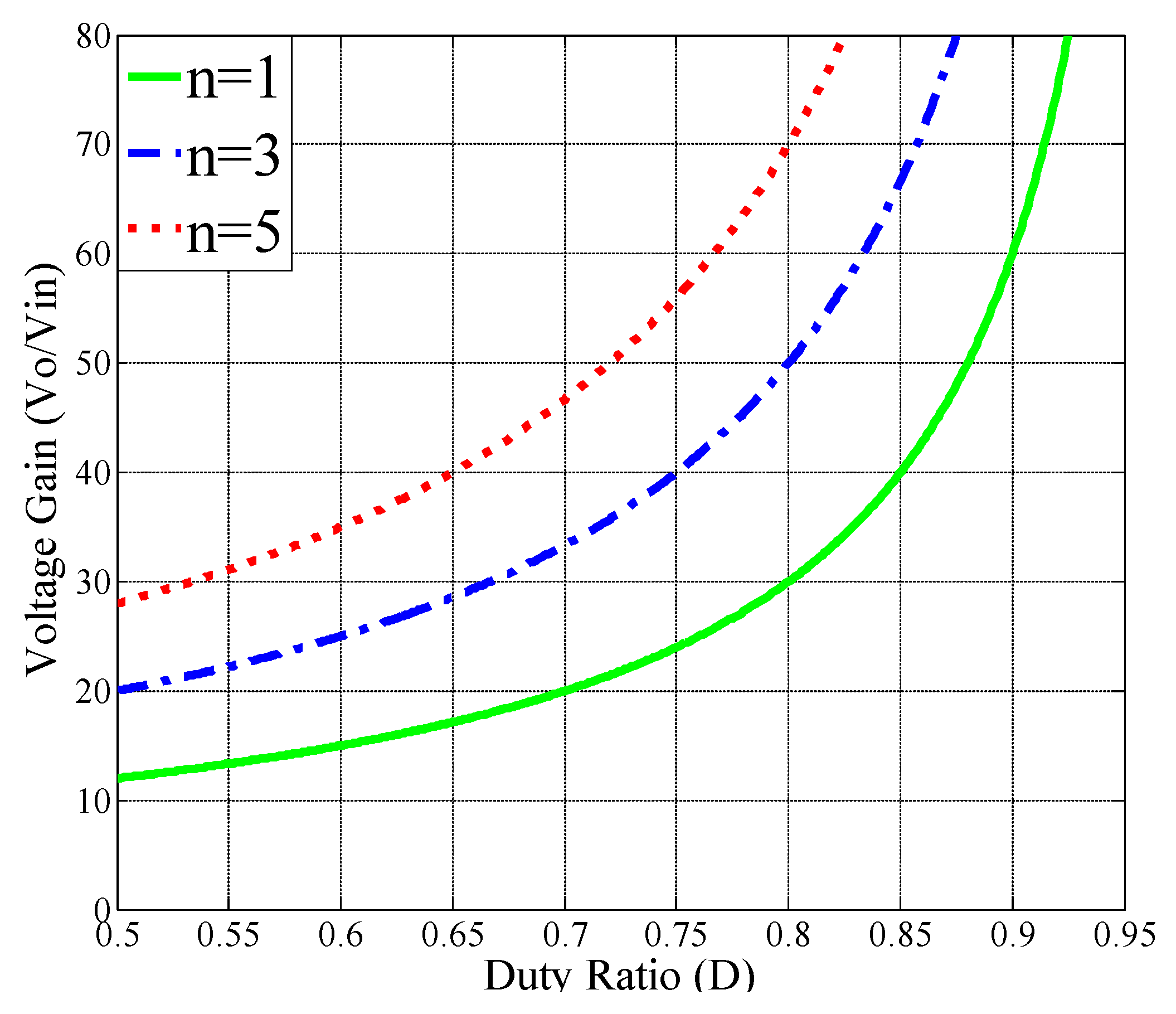
3.1. Voltage Gain
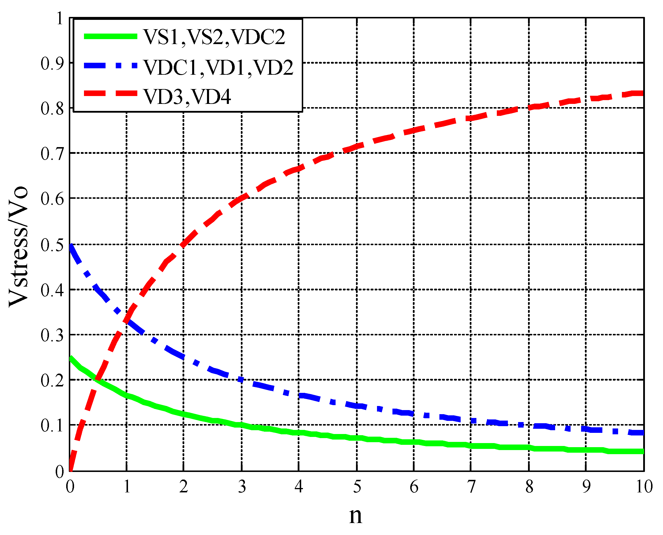
3.2. Voltage Stresses on Semiconductor Devices
3.3. Design Guidelines
3.3.1. Turns Ratio Design
3.3.2. Power Switches and Diodes Selection
3.3.3. Coupled Inductor Design
3.3.4. Capacitor Design
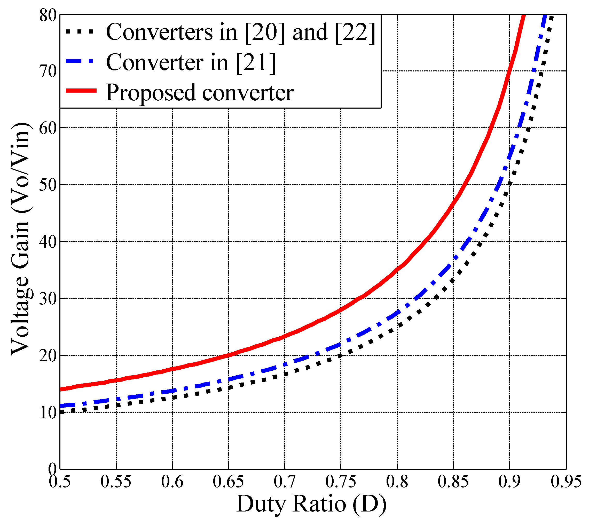
3.4. Performance Comparison
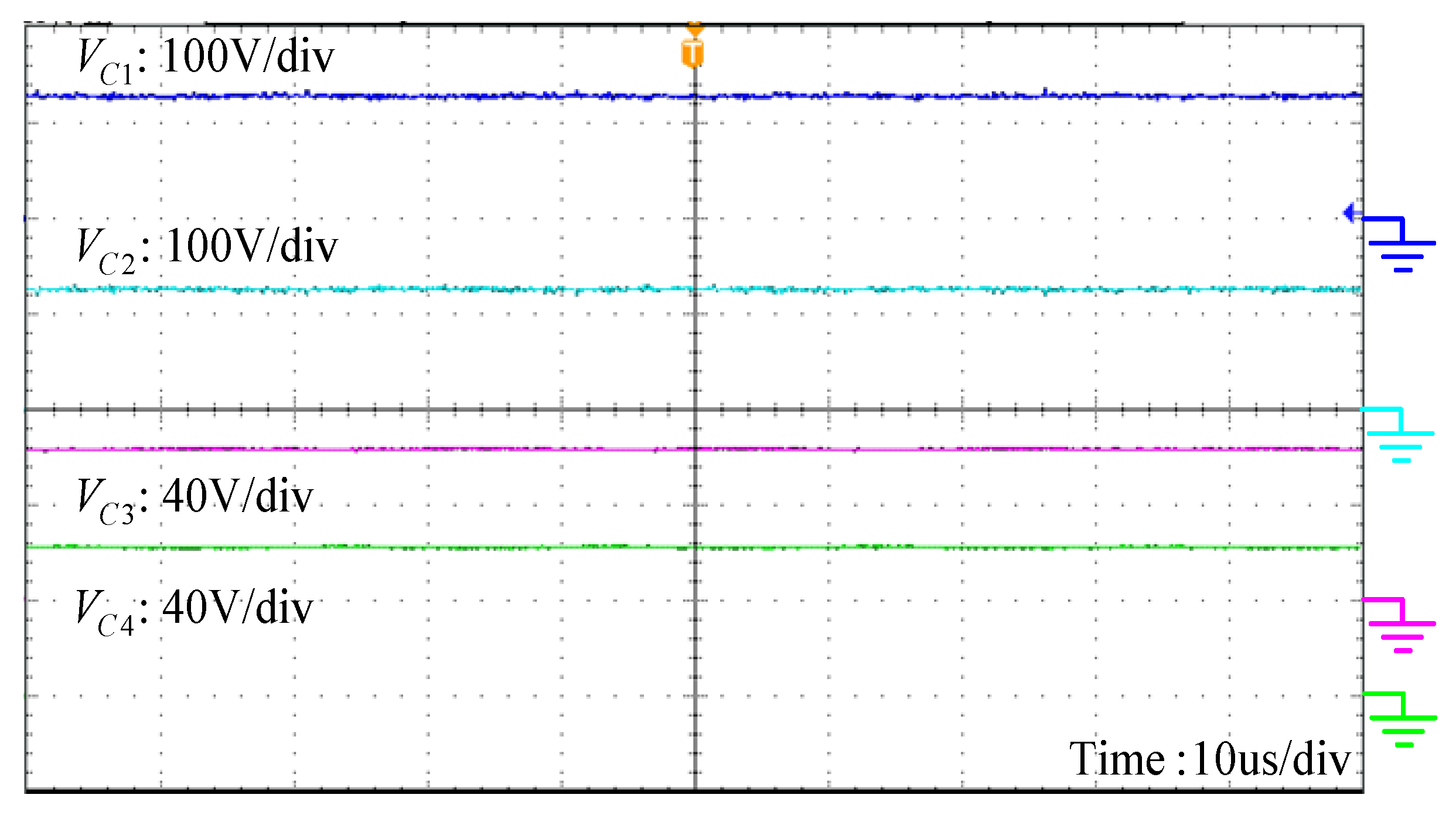
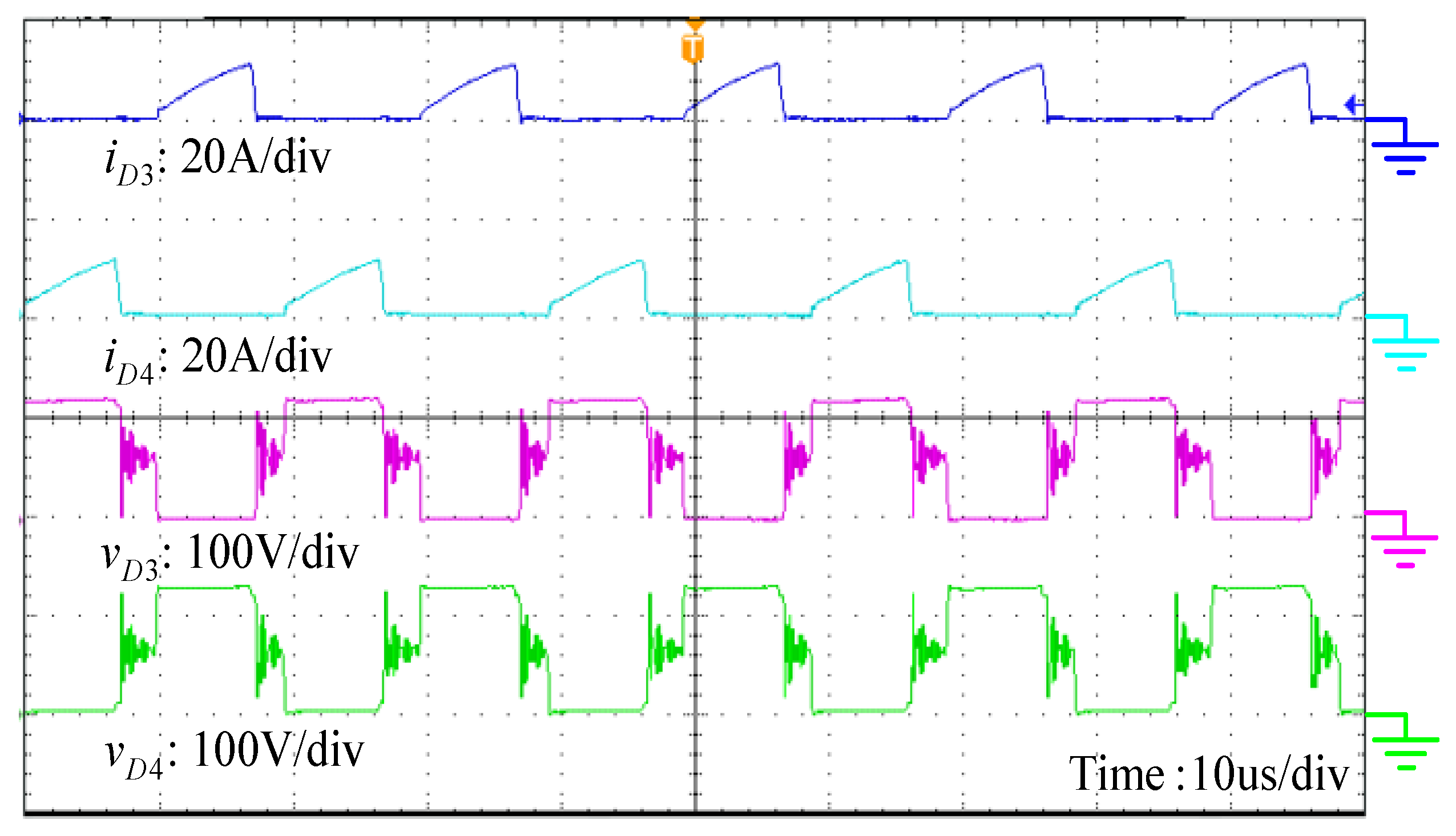
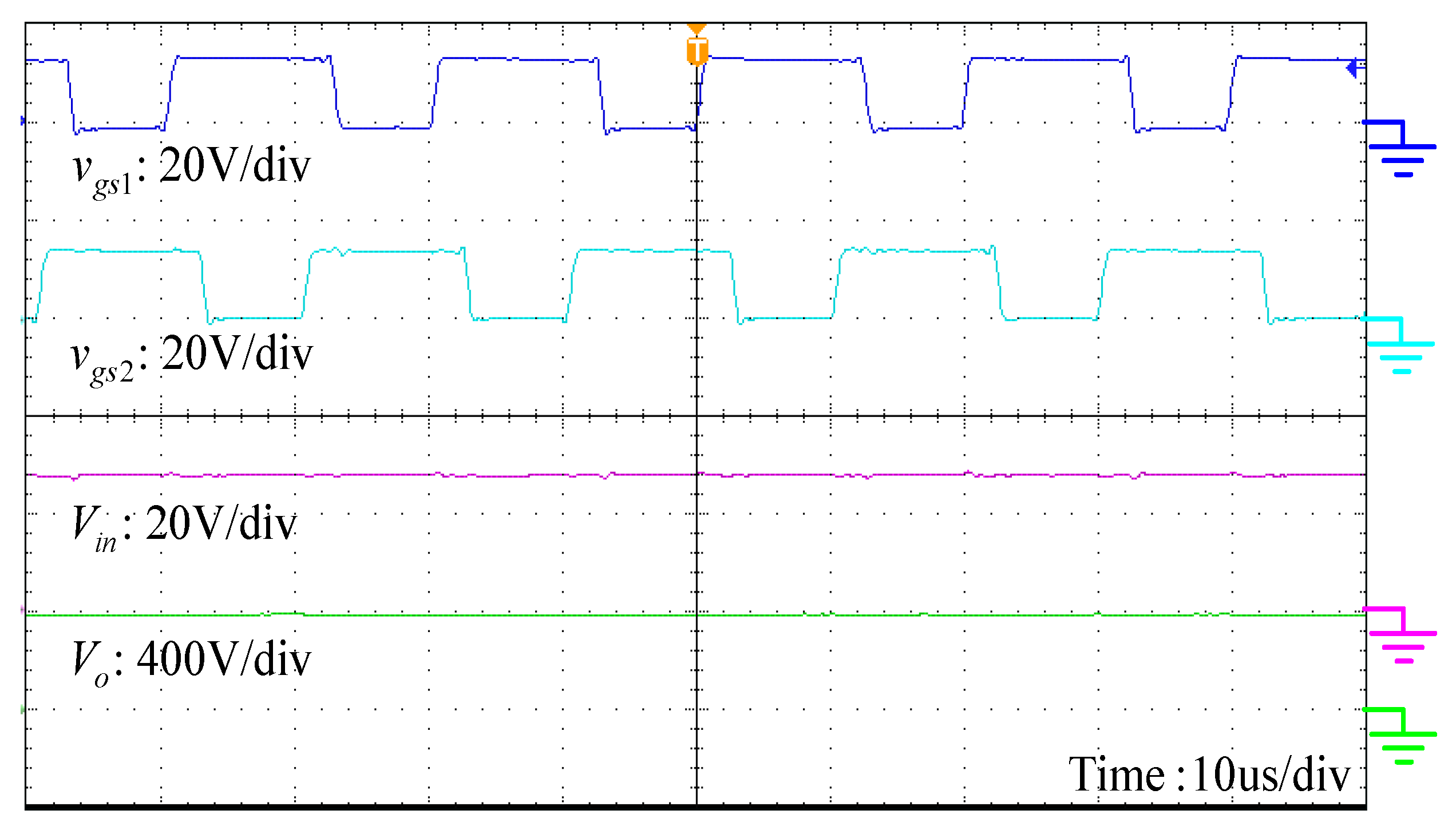
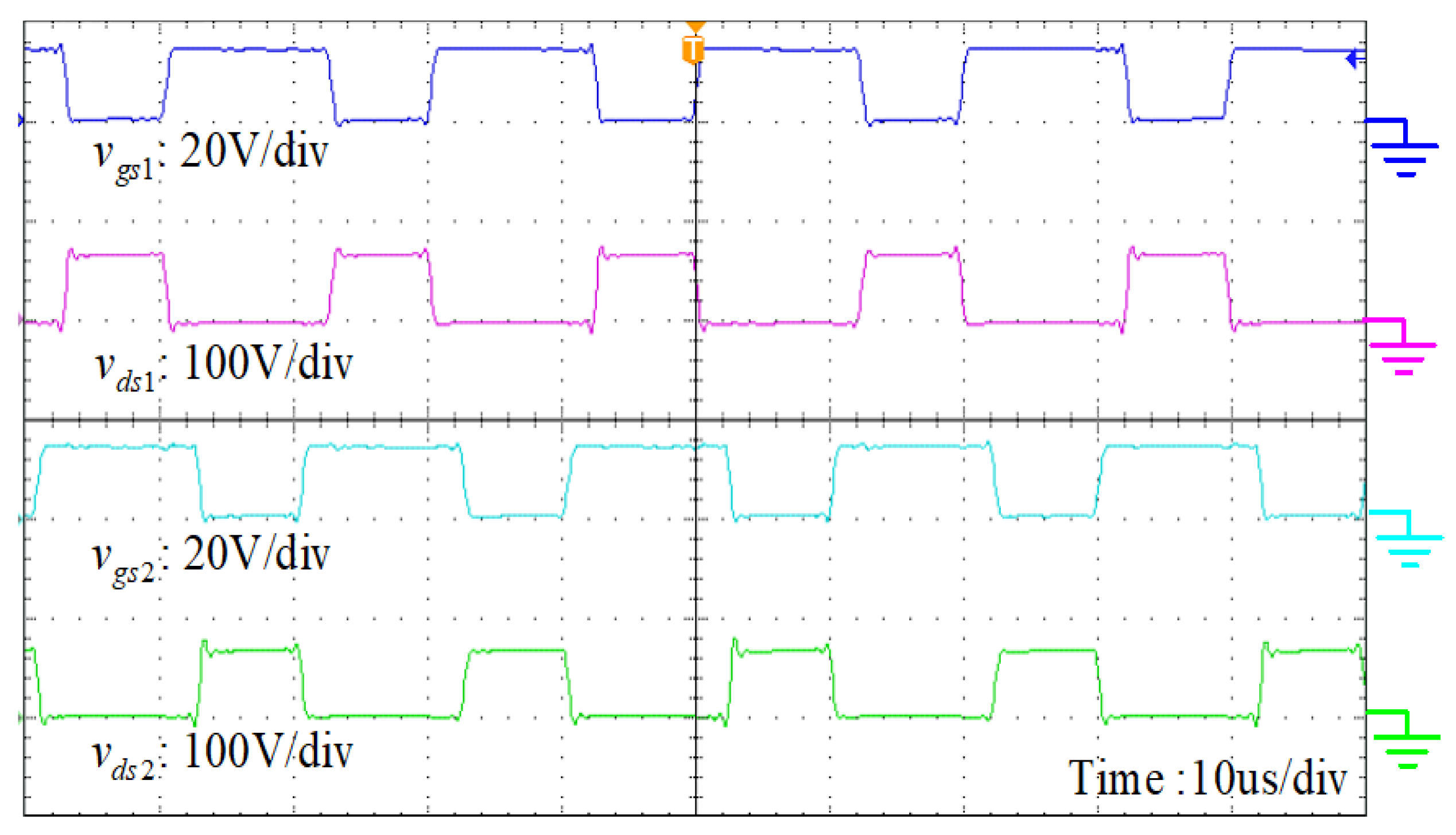
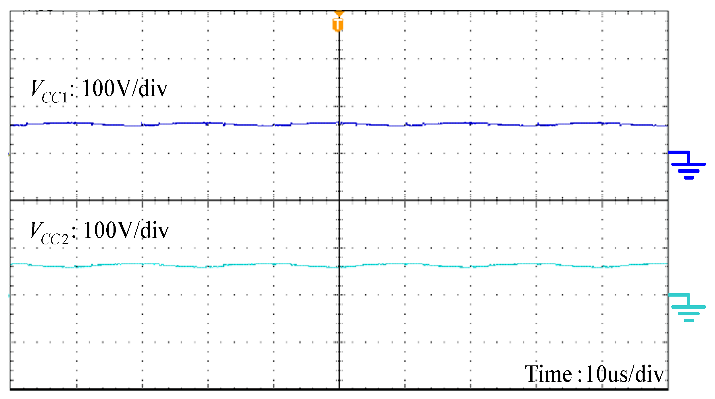
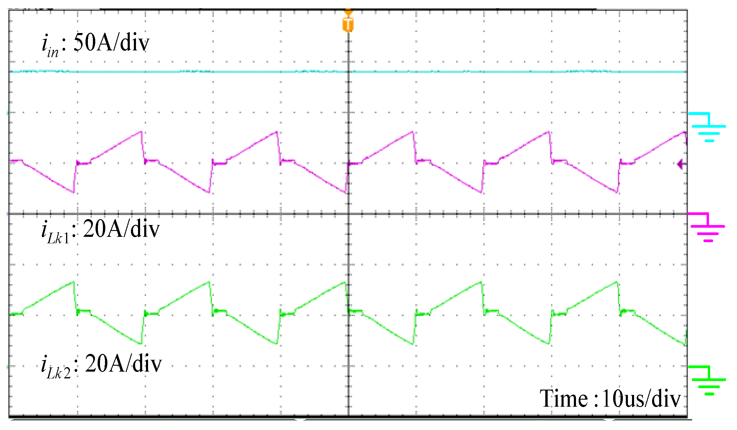
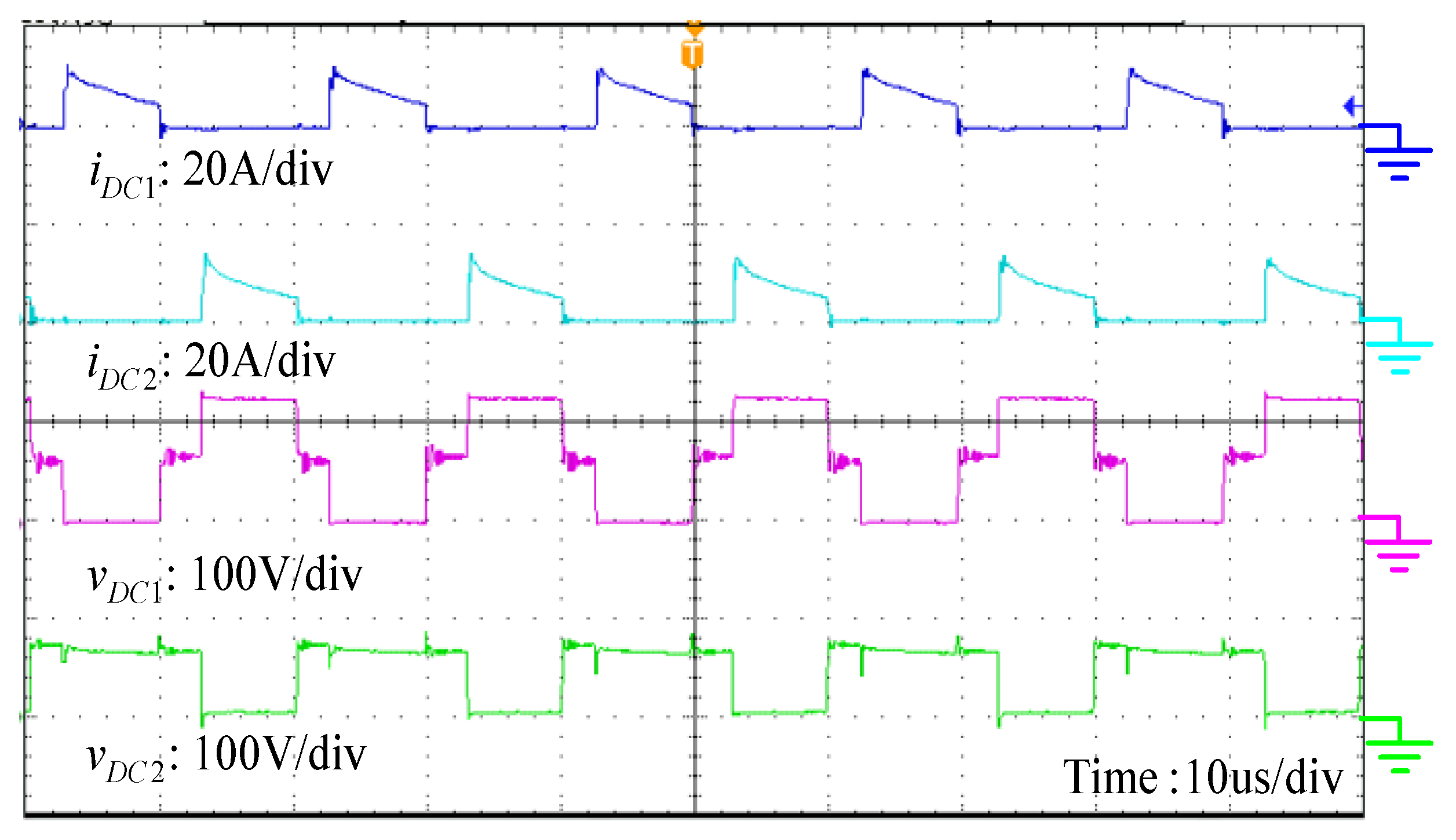
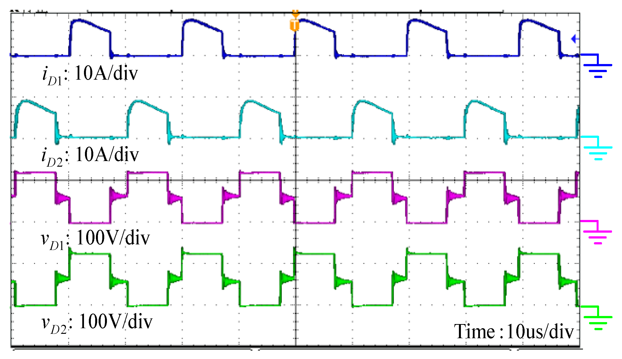
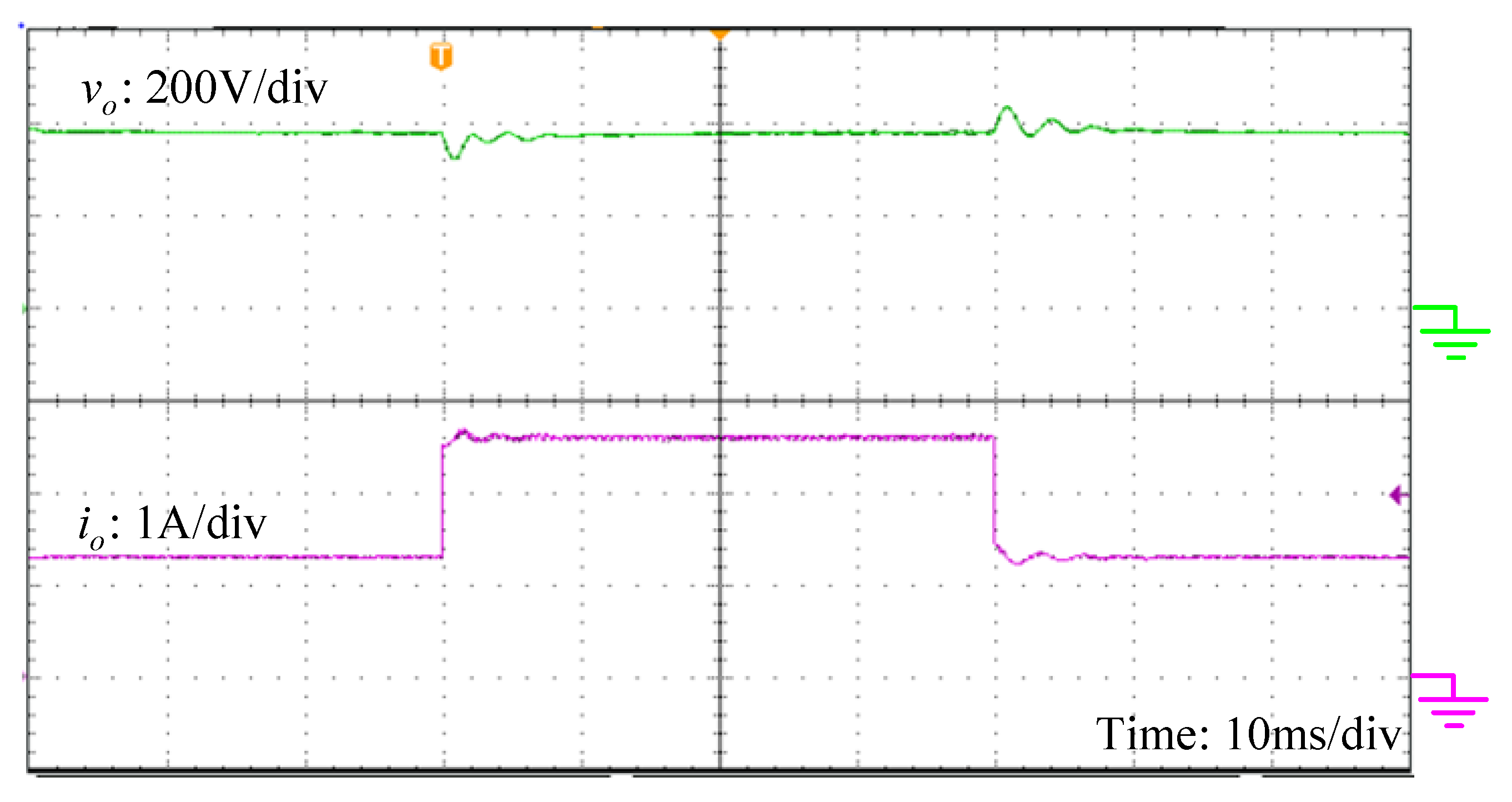
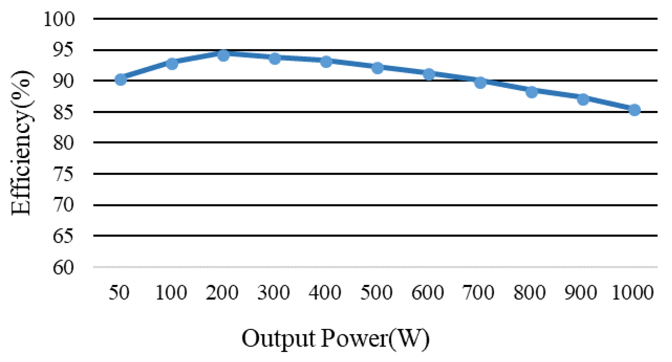
4. Experimental Verifications
5. Conclusions
Author Contributions
Funding
Conflicts of Interest
References
- Yang, B.; Li, W.; Zhao, Y.; He, X. Design and analysis of a grid connected PV power system. IEEE Trans. Power Electron. 2010, 25, 992–1000. [Google Scholar] [CrossRef]
- Carrasco, J.M.; Franquelo, L.G.; Bialasiewicz, J.T.; Galvan, E.; Guisado, R.C.P.; Prats, M.A.M.; Leon, J.I.; Moreno-Alfonso, N. Power-electronic systems for the grid integration of renewable energy sources: A survey. IEEE Trans. Ind. Electron. 2006, 53, 1002–1016. [Google Scholar] [CrossRef]
- Arunkumari, T.; Indragandhi, V. An overview of high voltage conversion ratio dc-dc converter configurations used in DC micro-grid architectures. Renew. Sustain. Energy Rev. 2017, 77, 670–687. [Google Scholar] [CrossRef]
- Ajami, A.; Ardi, H.; Farakhor, A. A novel high step-up DC-DC converter based on integrating coupled inductor and switched-capacitor techniques for renewable energy applications. IEEE Trans. Power Electron. 2015, 30, 4255–4263. [Google Scholar] [CrossRef]
- Tofoli, F.L.; Pereira, D.C.; Paula, W.J.; Junior, D.S.O. Survey on non-isolated high-voltage step-up DC–DC topologies based on the boost converter. IET Power Electron. 2015, 8, 2044–2057. [Google Scholar] [CrossRef]
- Hsieh, Y.P.; Chen, J.F.; Liang, T.J.; Yang, L.S. Novel high step-up dc-dc converter with coupled-inductor and switched-capacitor techniques for a sustainable energy system. IEEE Trans. Power Electron. 2011, 26, 3481–3490. [Google Scholar] [CrossRef]
- Honarjoo, B.; Madani, S.M.; Niroomand, M.; Adib, E. Analysis and Implementation of a New Single Switch, High Voltage Gain DC-DC Converter with a Wide CCM Operation Range and Reduced Components Voltage Stress. J. Power Electron. 2018, 18, 11–22. [Google Scholar]
- Hu, X.; Gong, C. A high voltage gain DC-DC converter integrating coupled-inductor and diode-capacitor techniques. IEEE Trans. Power Electron. 2014, 29, 789–800. [Google Scholar]
- Liu, H.; Ai, J.; Li, F. A novel high step-up converter with a switched-coupled-inductor-capacitor structure for sustainable energy systems. J. Power Electron. 2016, 16, 436–446. [Google Scholar] [CrossRef]
- Wong, Y.S.; Chen, J.F.; Liu, K.B.; Hsieh, Y.P. A novel high step-up DC-DC converter with coupled inductor and switched clamp capacitor techniques for photovoltaic systems. Energies 2017, 10, 378. [Google Scholar] [CrossRef]
- Wei, C.L.; Shih, M.H. Design of a switched-capacitor DC-DC converter with a wide input voltage range. IEEE Trans. Circuits Syst. 2013, 60, 1648–1656. [Google Scholar] [CrossRef]
- Chung, H.S.; Ioinovici, A.; Cheung, W.L. Generalized structure of bi-directional switched-capacitor dc/dc converters. IEEE Trans. Circuits Syst. I 2003, 50, 743–753. [Google Scholar] [CrossRef]
- Yang, L.S.; Liang, T.J.; Chen, J.F. Transformerless DC-DC Converters with high step-up voltage gain. IEEE Trans. Ind. Electron. 2009, 56, 3144–3152. [Google Scholar] [CrossRef]
- Pan, C.T.; Chuang, C.F.; Chu, C.C. A Novel transformer-less adaptable voltage quadrupler dc converter with low switch voltage stress. IEEE Trans. Power Electron. 2014, 29, 4787–4796. [Google Scholar] [CrossRef]
- Tseng, K.C.; Chen, C.T.; Cheng, C.A. A high-efficiency high step-up interleaved converter with a voltage multiplier for electric vehicle power management applications. J. Power Electron. 2016, 16, 414–424. [Google Scholar] [CrossRef]
- Prudente, M.R.; Pfitscher, L.L.; Emmendoerfer, G.; Romaneli, E.F.; Gules, R. Voltage multiplier cells applied to non-isolated converters. IEEE Trans. Power Electron. 2008, 23, 871–887. [Google Scholar] [CrossRef]
- Li, W.; Zhao, Y.; Deng, Y.; He, X. Interleaved converter with voltage multiplier cell for high step-up and high efficiency conversion. IEEE Trans. Power Electron. 2010, 25, 2397–2408. [Google Scholar] [CrossRef]
- Tseng, K.C.; Huang, C.C. High step-up high-efficiency interleaved converter with voltage multiplier module for renewable energy system. IEEE Trans. Ind. Electron. 2014, 61, 1311–1319. [Google Scholar] [CrossRef]
- Shen, C.L.; Chiu, P.C.; Lee, Y.C. Novel interleaved converter with extra-high voltage gain to process low-voltage renewable-energy generation. Energies 2016, 9, 871–882. [Google Scholar] [CrossRef]
- Li, W.; Zhao, Y.; Wu, J.; He, X. Interleaved high step-up converter with winding-cross-coupled inductors and voltage multiplier cells. IEEE Trans. Power Electron. 2012, 27, 133–143. [Google Scholar] [CrossRef]
- Nouri, T.; Hosseini, S.H.; Babaei, E.; Ebrahimi, J. Interleaved high step-up DC-DC converter based on three-winding high-frequency coupled inductor and voltage multiplier cell. IET Power Electron. 2015, 8, 175–189. [Google Scholar] [CrossRef]
- He, L.; Liao, Y. An advanced current-autobalance high step-up converter with a multicoupled inductor and voltage multiplier for a renewable power generation system. IEEE Trans. Power Electron. 2016, 31, 6992–7005. [Google Scholar]
- Cao, L. Type III compensator design for power converters. Power Electron. Technol. 2011, 1, 20–25. [Google Scholar]


| Topology | Converter Published in [20] | Converter Published in [21] | Converter Published in [22] | Proposed Converter |
|---|---|---|---|---|
| Voltage gain | ||||
| Voltage stress on switches | ||||
| The highest voltage stress on diodes | ||||
| Switches | 2 | 2 | 2 | 2 |
| Diodes | 6 | 8 | 6 | 6 |
| Capacitors | 5 | 7 | 5 | 6 |
| Coupled inductors | 2 | 2 | 2 | 2 |
| Components | Parameters |
|---|---|
| Input voltage Vin | 28 V |
| Output voltage Vo | 380 V |
| Maximum output power Po | 1000 W |
| Switching frequency fs | 50 kHz |
| Magnetizing inductances Lm1 and Lm2 | 245 µH |
| Leakage inductances Lk1 and Lk2 | 0.9 µH |
| Turns ratio n | 1 |
| Switches S1 and S2 | IRFP4321 |
| Diodes DC1, DC2, D1, D2, D3, D4 | 30CPQ200 |
| Clamp capacitors CC1 and CC2 | 10 µF |
| Output capacitors C1 and C2 | 100 µF |
| Switched capacitors C3 and C4 | 100 µF |
© 2018 by the authors. Licensee MDPI, Basel, Switzerland. This article is an open access article distributed under the terms and conditions of the Creative Commons Attribution (CC BY) license (http://creativecommons.org/licenses/by/4.0/).
Share and Cite
Chen, S.-J.; Yang, S.-P.; Huang, C.-M.; Chou, H.-M.; Shen, M.-J. Interleaved High Step-Up DC-DC Converter Based on Voltage Multiplier Cell and Voltage-Stacking Techniques for Renewable Energy Applications. Energies 2018, 11, 1632. https://doi.org/10.3390/en11071632
Chen S-J, Yang S-P, Huang C-M, Chou H-M, Shen M-J. Interleaved High Step-Up DC-DC Converter Based on Voltage Multiplier Cell and Voltage-Stacking Techniques for Renewable Energy Applications. Energies. 2018; 11(7):1632. https://doi.org/10.3390/en11071632
Chicago/Turabian StyleChen, Shin-Ju, Sung-Pei Yang, Chao-Ming Huang, Huann-Ming Chou, and Meng-Jie Shen. 2018. "Interleaved High Step-Up DC-DC Converter Based on Voltage Multiplier Cell and Voltage-Stacking Techniques for Renewable Energy Applications" Energies 11, no. 7: 1632. https://doi.org/10.3390/en11071632
APA StyleChen, S.-J., Yang, S.-P., Huang, C.-M., Chou, H.-M., & Shen, M.-J. (2018). Interleaved High Step-Up DC-DC Converter Based on Voltage Multiplier Cell and Voltage-Stacking Techniques for Renewable Energy Applications. Energies, 11(7), 1632. https://doi.org/10.3390/en11071632