Article

High-Efficiency Isolated Photovoltaic Microinverter Using Wide-Band Gap Switches for Standalone and Grid-Tied Applications

1
Department of Electrical Engineering, National Ilan University, No. 1, Section 1, Shennong Road, Yilan 260, Taiwan
2
Department of Electronic Engineering, National Taiwan University of Science and Technology, No. 43, Section 4, Keelung Road, Da’an District, Taipei 106, Taiwan
3
School of Electrical and Computer Engineering, Ulsan National Institute of Science and Technology, 50 UNIST-gil Ulju-gun, Ulsan 44919, Korea
*
Author to whom correspondence should be addressed.
Energies 2018, 11(3), 569; https://doi.org/10.3390/en11030569
Submission received: 6 February 2018 / Revised: 28 February 2018 / Accepted: 28 February 2018 / Published: 6 March 2018
(This article belongs to the Special Issue Power Electronics in DC-Microgrid Systems)

Abstract

:
An isolated photovoltaic micro-inverter for standalone and grid-tied applications is designed and implemented to achieve high efficiency. System configuration and design considerations, including the proposed active-clamp forward-flyback resonant converter for the DC-DC stage and a dual-frequency full-bridge inverter for the DC-AC stage, are analyzed and discussed. A prototype microinverter system is built and tested. Experimental results verify the feasibility of the proposed system, which achieves 95% power conversion efficiency at full load.

1. Introduction

Photovoltaic (PV) energy systems have been extensively studied in research and industries as an alternative to fossil fuels to reduce greenhouse effects [1,2,3]. The concept of maximum power point tracking (MPPT) is used to extract maximum solar power from PV panels [4,5]. Several PV panels are typically connected in series/parallel to provide high voltage/current for high-power applications. However, PV panels frequently work under mismatched conditions due to partial shading and variations in panel orientation [6,7,8]. Thus, the power production of an entire PV string is reduced by this mismatching issue. One way to address the mismatch problem in large strings is to employ MPPT at the individual panel level using microinverters. Figure 1 shows the system diagram of the isolated PV microinverter mounted on each PV panel [9,10,11]. The pre-stage DC-DC converter provides isolation and controls the PV panel to extract its maximum power and provides a high-voltage DC bus for the post-stage DC-AC inverter [12,13,14]. The inverter converts the DC voltage into a sinusoidal AC output voltage that connects and supplies power to the AC-grid system [15].
One problem with conventional solar microinverters is their poor conversion efficiency mainly attributed the hard-switching operation of the power converter. The commercial success of a PV microinverter depends on its reliability and efficiency. However, high device stress and hard switching operation results in low conversion efficiency. A PV microinverter with a pseudo DC-link is advantageous because it can achieve high efficiency. However, the component count and control complexity are high such that the overall system reliability is decreased [16,17,18].
Wide band-gap (WBG) materials such as Silicon Carbide (SiC) and Gallium Nitride (GaN) have attracted increasing attention in switching power supply applications [19,20,21]. Compared with the current Silicon (Si) technology, WBG devices provide significant advantages of high operating temperature, fast switching speed, and low on-resistance. Thus, they can reduce switching losses to enable high-frequency operation and achieve high-efficiency performance.
This work presents a highly efficient grid-tied isolated PV microinverter that can individually extract the maximum solar power to transfer power to the AC utility network. This work focuses on implementing a two-stage topology. The active-clamp forward-flyback converter topology is adopted for the front-end of the system, which converts energy from the PV panel to a higher voltage for the post-stage inverter. The proposed active-clamp forward-flyback converter topology combines the concepts of forward and flyback converters to increase the utilization of the flyback transformer, while the resonant mechanism is added to the converter unit design. The resonant aspect brings the benefits of extending the zero-voltage-switching (ZVS) region and allowing the secondary diodes to achieve zero-current-switching (ZCS). Furthermore, the fixed frequency pulse-width modulation (PWM) can be achieved to control the converter by only changing the component value. It retains the advantages of high efficiency and easy of control. The microinverter is implemented with WBG devices for PV panel applications to achieve low harmonic distortion, small circuit size and high efficiency. The contributions of this work are: (1) the introduction and analysis of the resonant control strategy of the active-clamp forward-flyback converter to allow for ZVC and ZCS to reduce losses, and (2) the implementation and experimental validation of the interleaved active-clamp forward-flyback converter using WBG devices to achieve a highly-efficiency PV microinverter.

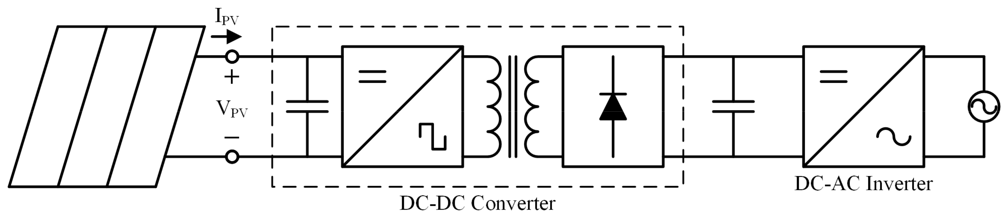
2. System Design and Considerations

The proposed system configuration consists of an interleaved active-clamped forward-flyback converter for the DC-DC stage and a dual-frequency full-bridge inverter for the DCAC stage, as shown in Figure 2. The inverter can operate in a standalone mode (also called grid forming mode), where the inverter is not connected to the AC electric grid, or in an on-grid mode (also called grid feeding mode), where PV power is supplied to the AC electric grid [22]. The control of each converter differs depending on the operation mode, which is further detailed in Section 2.2.
The detailed schematic of the interleaved active-clamped forward-flyback resonant converter and dual-frequency full-bridge circuit are shown in Figure 3. The first stage is the interleaved active-clamped forward-flyback resonant converter, whose characteristics are similar to those of forward resonant converter in the charging phase and the flyback resonant converter in the discharging phase. This topology has advantages of small size and low input current ripple. The active-clamped circuit is used to recycle energy stored by the leakage inductance of the coupled inductor and to reduce voltage stress on the switch. The DC-DC pre-stage circuit is operated in either single or interleaved mode depending on power conditions, which is used to improve light-load efficiency.
For the second stage, the dual-frequency full-bridge circuit is selected because it produces a wider output voltage range for the same input voltage and also reduces the current stress on the switch. The dual-frequency full-bridge circuit exhibits the important advantage of improved efficiency because of the single arm-chopped waveform action, as shown in Figure 4. This feature nearly eliminates the switching loss on one arm. Details of the proposed microinverter system and control strategy are covered in the next section.

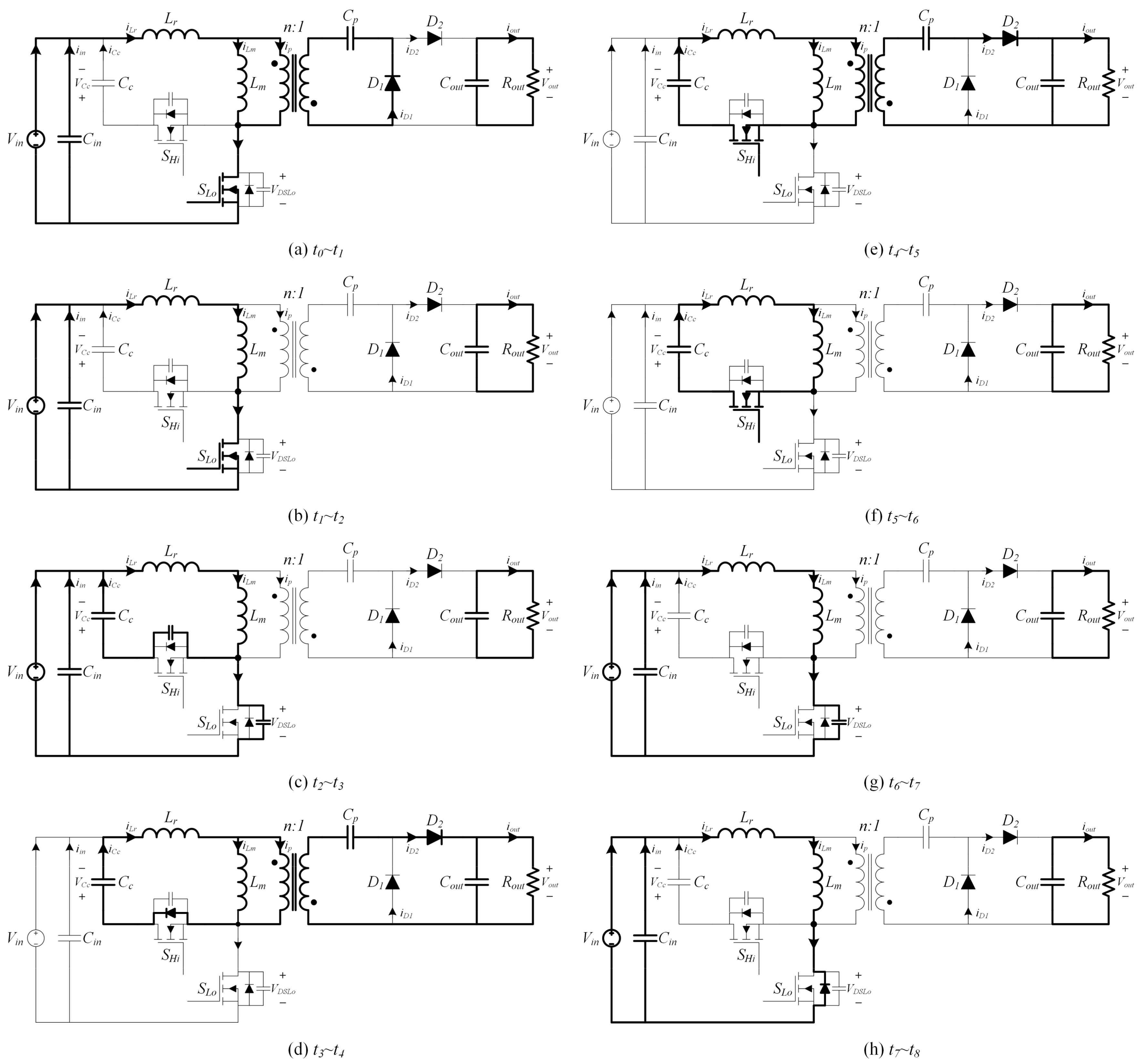
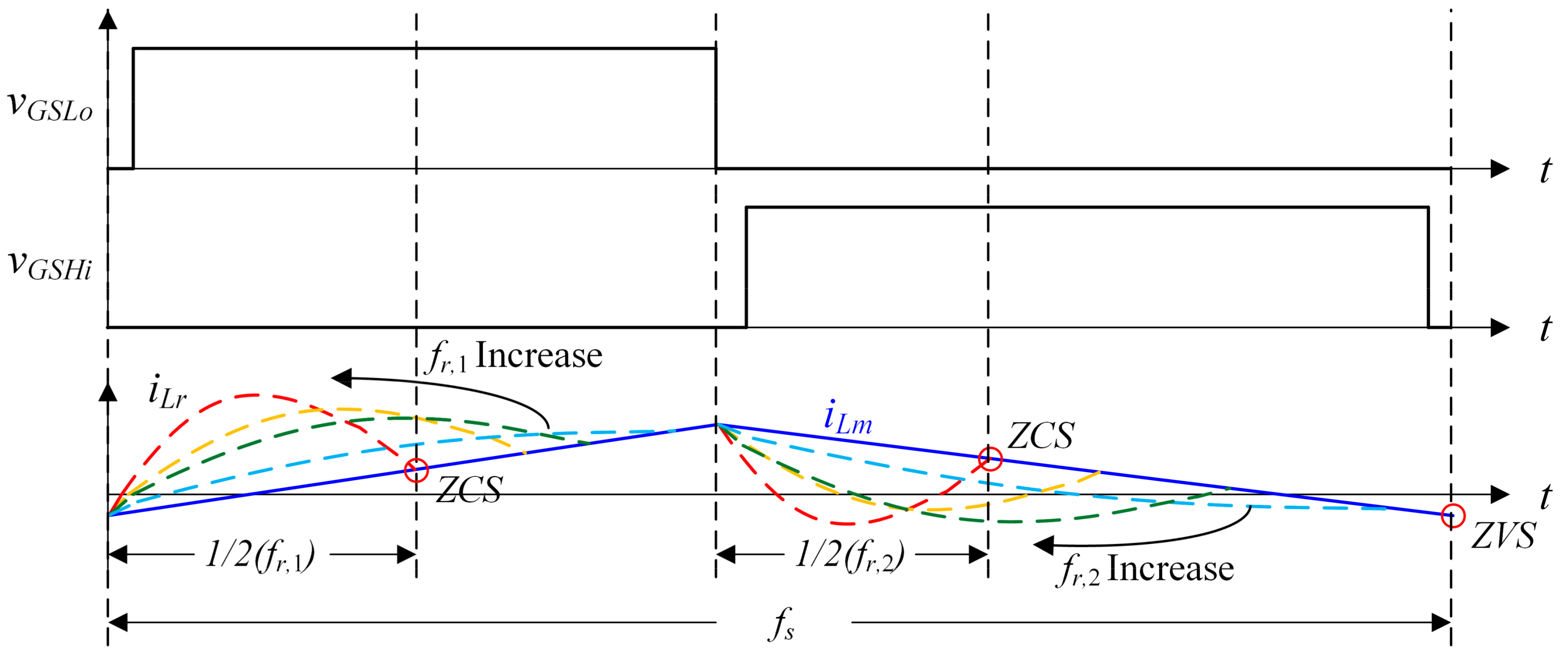
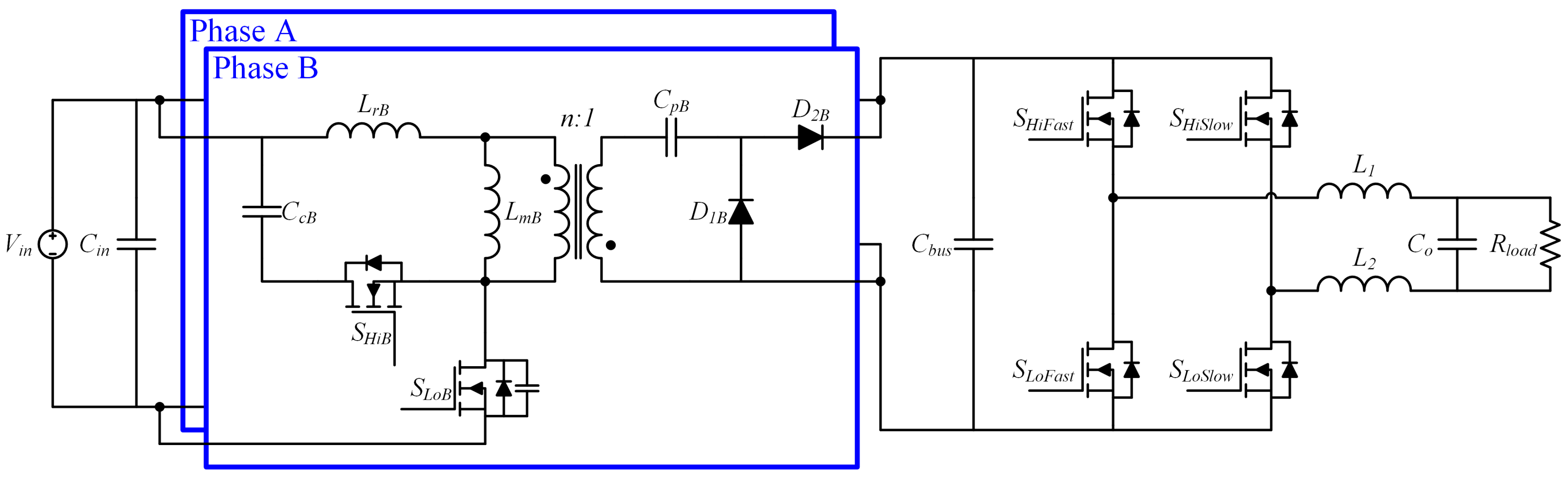
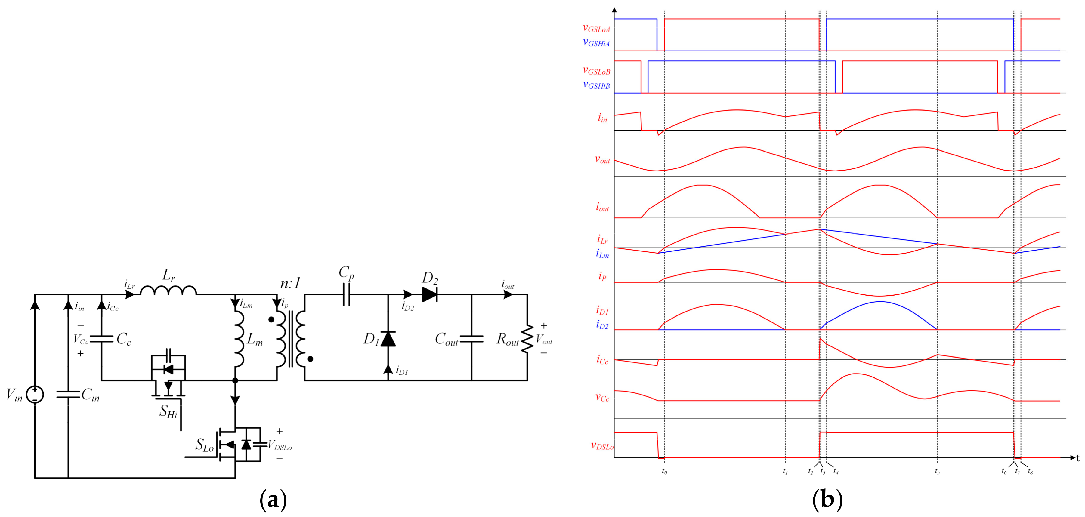
2.1. Active-Clamp Forward-Flyback Resonant Converter
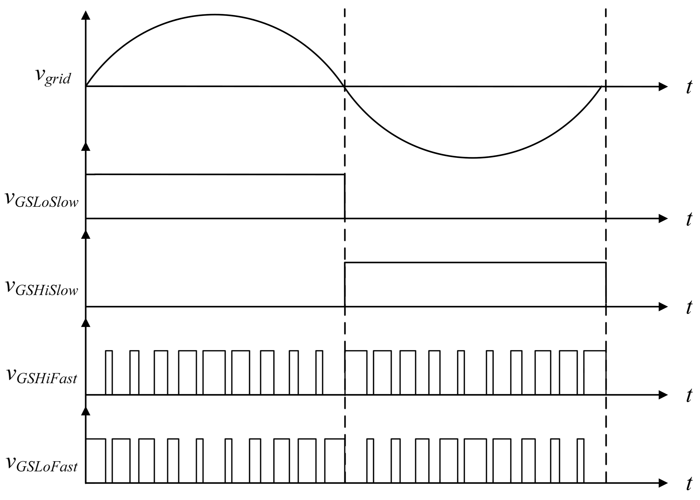
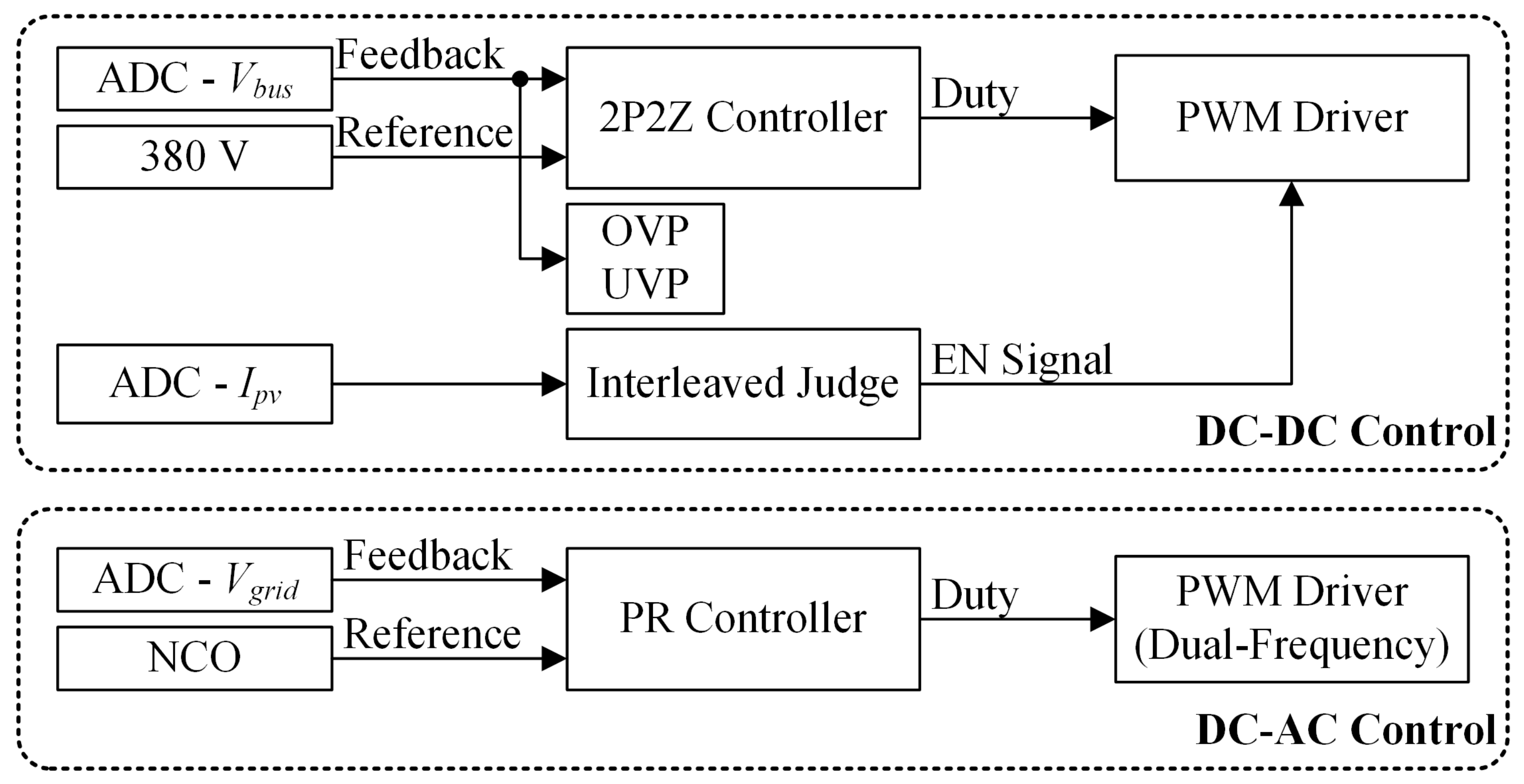
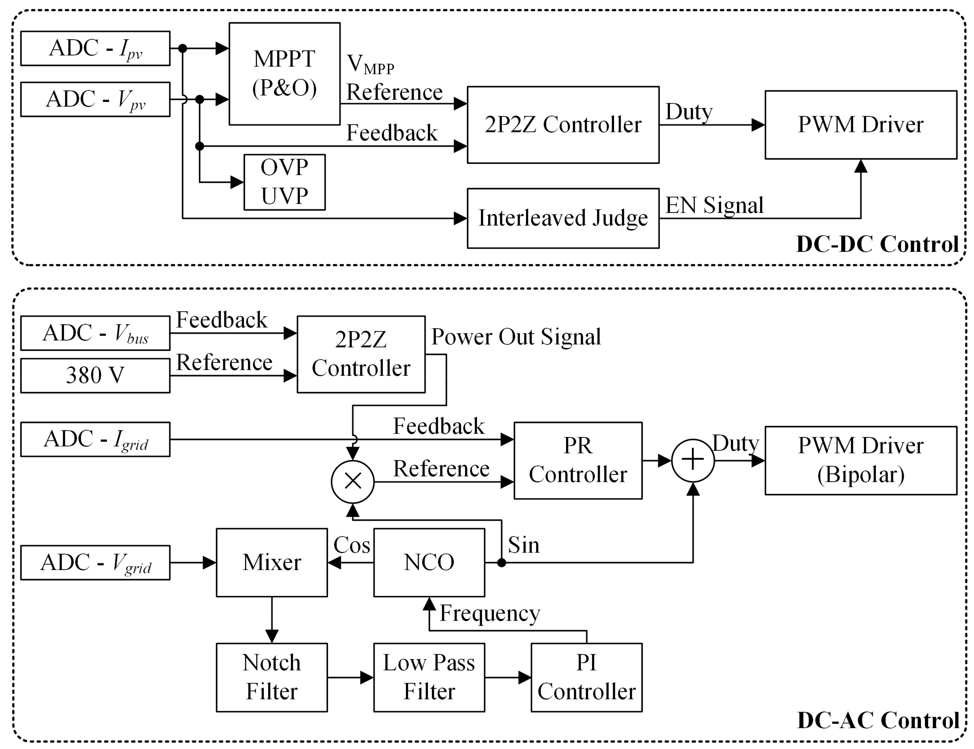
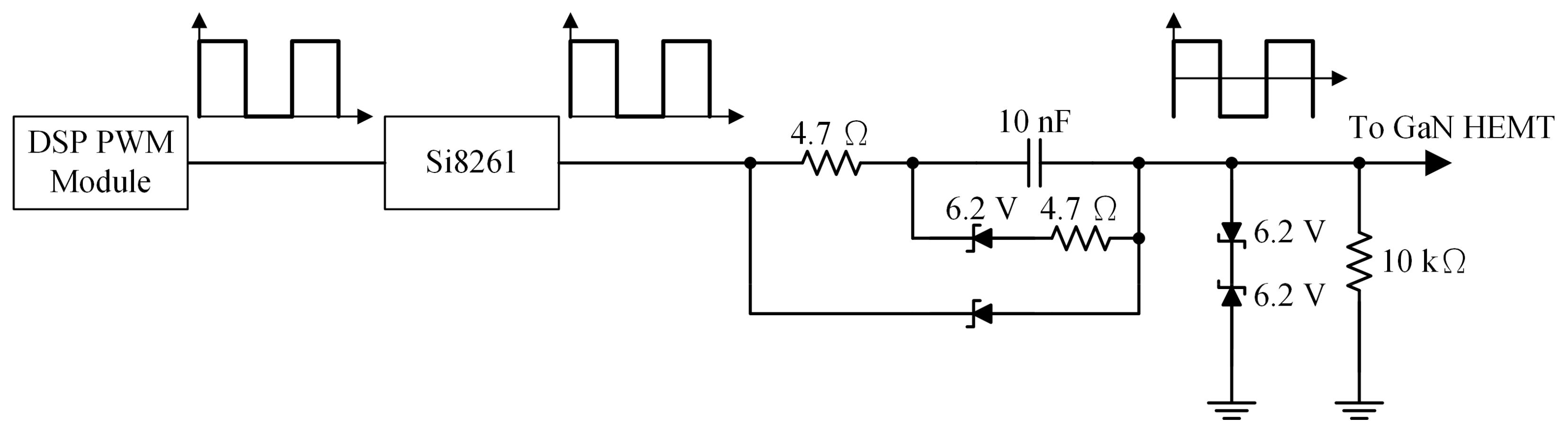
Under steady-state operation, the active-clamped forward-flyback resonant converter undergoes eight switching states. Figure 5a shows the circuit schematics and Figure 5b shows the theoretical waveforms.
As shown in Figure 6, the circuit principles of the DC-DC converter stage are analyzed and discussed in detail. A capacitor is placed in parallel with the PV panel such that the PV voltage is relatively constant over the full cycle of the period. Thus, Vin is assumed to be constant for the following analysis. Eight states are described for time t over a full cycle.
State 1 (t0t1): During this time interval, the auxiliary switch SHi is off. The main switch SLo is turned on with zero-voltage switching (ZVS) at t0 because of the conduction of its body diode. At the secondary side, the diode D1 is on and D2 is off. Load power is supplied alone by the output capacitor Cout. The leakage inductance Lr resonates with capacitor Cp. The resonant current iLr can be represented as follows:
i L r ( t ) = i L m ( t ) + i p ( t ) i L r ( t 0 ) + V i n L m + L r ( t t 0 ) + i p ( t )
i p ( t ) = V i n Z 0 sin ω 0 ( t t 0 )
where Lm is the magnetizing inductance and iLm is its current, ip is the primary transformer current, and Vin is the input voltage. Resonant angular frequency ω0 is defined as
ω 0 = 1 L r ( C p / n 2 )
where n is the transformer turns ratio, and impedance Z0 is defined as
Z 0 = L r ( C p / n 2 ) .
State 2 (t1t2): The transformer primary current reaches zero at t1, and the diode D1 is off with zero-current switching (ZCS). During this time interval, D2 remains turned off and the load power is still supplied only by output capacitor Cout. The resonant current iLr can be represented as follows:
i L r ( t ) = i L m ( t ) = i L r ( t 1 ) + V i n L m + L r ( t t 1 ) .
State 3 (t2t3): The main switch SLo is turned off at t2, and the equivalent inductor (Lm + Lr) resonates with SLo D-S capacitor CDSLo. The resonant current iLr and resonant voltage vDSLo can be represented as follows:
i L r ( t ) = V i n Z 2 sin ω 2 ( t t 2 ) + i L r ( t 2 ) cos ω 2 ( t t 2 )
v D S L o ( t ) V i n [ 1 cos ω 2 ( t t 2 ) ] + i L r ( t 2 ) Z 2 sin ω 2 ( t t 2 )
where resonant angular frequency ω2 is defined as
ω 2 = 1 ( L m + L r ) C D S L o
and impedance Z2 is defined as
Z 2 = ( L m + L r ) C D S L o .
State 4 (t3t4): The resonant voltage vDSLo reaches (Vin + vC) at t4, and the body diode of the auxiliary switch SHi and output diode D2 are turned on. The resonant current iLr, the transformer primary current ip and diode D2 current iD2 can be represented as follows:
i L r ( t ) = i L m ( t ) + i p ( t ) i L m ( t 3 ) v L m ( t ) L m + i L r ( t 3 ) cos ω 3 ( t t 3 )
i p ( t ) i L r ( t 3 ) cos ω 3 ( t t 3 )
i D 2 ( t ) = n i p ( t )
where resonant angular frequency ω3 is defined as
ω 3 = 1 L r C e q
equivalent capacitance Ceq is defined as
C e q = C c · ( C p / n 2 ) C c + ( C p / n 2 )
and Cc is the clamping capacitor.
State 5 (t4t5): During this time interval, the main switch SLo remains turned off. The auxiliary switch SHi is turned on with ZCS at t4. The circuit equations are the same with those during State 4.
State 6 (t5t6): The transformer primary current reaches zero at t5. The output diode D2 is turned off with ZCS and the load power is supplied only by the output capacitor Cout. The resonant current iLr is as follows:
i L r ( t ) i L r ( t 5 ) cos ω 5 ( t t 5 ) + v C C ( t 5 ) Z 5 sin ω 5 ( t t 5 )
where resonant angular frequency ω4 is defined as
ω 5 = 1 ( L r + L m ) C c
and impedance Z5 is defined as
Z 5 = ( L r + L m ) C c .
State 7 (t6t7): The auxiliary switch SHi is turned off at t6. During this time interval, the energy stored in SLo D-S capacitor CDSLo is released by the resonance with the equivalent inductor (Lm + Lr). The resonant current iLr and voltage vDSLo can be represented as follows:
i L r ( t ) = i L r ( t 6 ) cos ω 6 ( t t 6 ) + [ V i n v D S L o ( t 6 ) ] Z 6 sin ω 6 ( t t 6 )
v D S L o ( t ) = V i n [ V i n v D S L o ( t 6 ) ] cos ω 6 ( t t 6 ) + i L r ( t 6 ) Z 6 sin ω 6 ( t t 6 )
where resonant angular frequency ω6 is defined as
ω 6 = 1 ( L r + L m ) C D S L o
and impedance Z6 is defined as
Z 6 = L r + L m C D S L o .
State 8 (t7t8): The resonant voltage vDSLo is reduced to zero at t7 and the body diode of the main switch SLo conducts to achieve ZVS. The resonant current iLr is as follows:
i L r ( t ) = i L r ( t 7 ) + V i n L r + L m ( t t 7 ) .
After completing one switching period, the operation mode starts over from State 1. The detailed resonant waveforms are depicted in Figure 7. The ZCS conditions for diode D1 is
T o n , 1 > 1 / 2 f r , 1 = π L r ( C p n 2 )
and the ZCS conditions for D2 is
T o n , 2 > 1 / 2 f r , 2 = π L r ( C c C p / n 2 C c + C p / n 2 )
where Ton,1 is the turn on time of SLo and fr,1 is its associated resonant frequency, and Ton,2 is the turn on time of SHi and fr,2 is its associated resonant frequency.

2.2. System Control

The microinverter used in this study has two operation modes: standalone and grid-tied operation. The system will automatically detect which mode to use. If the microinverter detects no voltage at the output terminal upon start-up, then it will operate in standalone mode. However, if a voltage is detected, then the microinverter will attempt to start the grid-tied mode operation. The control flowchart is shown in Figure 8.
In the standalone mode, the amount of power to be extracted from the solar panel is determined by the load demand. Therefore, the inverter and DC-DC stages will only be responsible for maintaining the correct voltage. The inverter will be in voltage-mode feedback, which ensures that the output voltage is a correctly-shaped sine wave with the correct amplitude. The voltage loop on the inverter stage uses proportional-resonant (PR) control to provide sufficient gain at 60 Hz output frequency. In this mode, it is particularly important to ensure good voltage regulation and low total harmonic distortion (THD). Meanwhile, the DC-DC stage regulates the bus voltage to ensure that the inverter has the correct voltage to work with. The block diagrams for the control in standalone mode for the DC-DC stage and DC-AC inverter stage are shown in Figure 9.
In the grid-tied mode, the unit decides how much power it will deliver to the grid. The duty of the DC-DC stage is to implement MPPT controller. The controller will attempt to deliver maximum power to the DC bus regardless of the bus voltage. Therefore, the inverter side has the task of maintaining the bus voltage. The inverter will have to deliver the same amount of power delivered to the bus to maintain the bus voltage at a constant value. The output voltage in grid-tied mode is dictated by the AC grid voltage; hence, the inverter will control the amount of current pumped into the grid. A feedback control loop is used for the inverter to achieve the current dictated by the reference. The grid-tied inverter requires that a sine wave with the same phase as the grid voltage be pumped into the grid. Thus, the input to the reference of the current loop is a numerically controlled oscillator (NCO). However, similar to the standalone mode, the gain at the AC-line frequency must be sufficient to ensure that the output follows the reference with accuracy. Thus, a PR control strategy is also implemented for the inverter’s current loop in grid-tied mode. The regulation requires that the output current signal must be in phase with the grid voltage. Therefore, certain mechanisms are necessary to produce a sine wave that is in phase with the output voltage. Accordingly, a phase-locked loop (PLL) that uses a phase detector is used to detect the phase difference between the output and input signals of the NCO. The phase difference is then fed through a controller, which will produce an output frequency signal given to the NCO. Consequently, a feedback loop in frequency is formed, which forces the NCO frequency to follow that of the grid voltage signal, as shown in Figure 10.
In addition to the PLL and current loop, the bus voltage must be kept at a constant value. This regulation task is handled by the inverter, which varies the current signal in order to control the voltage at the bus. A perturb and observe (P&O) method, which exhibits the benefits of simplicity and good performance, is adopted to realize MPPT for the DC-DC stage operated in grid-tied mode. The control black diagram for the DC-DC stage is also shown in Figure 10.

3. Results

3.1. Power Switch Comparison

GaN switches provide significant advantages over silicon (Si) metal oxide semiconductor field effect transistors (MOSFETs) with lower gate charge, smaller reverse recovery charge, and faster switching speeds. As outlined in Table 1, the GaN high electron mobility transistor (HEMT) presents much lower Figure of Merit (FOM), which is better than the conventional CoolMOS device. With much lower gate-charge Qg, the switching speed of the GaN HEMT device is much faster. Figure 11 shows the measured switching waveforms of Infineon CoolMOS 20N60CFD and Transphorm GaN HEMT TPH3006PS with Silicon Labs gate driver Si8261 and a 0-Ω gate resistor. In this work, 20N60CFD and TPH3006PS were tested and compared as high-frequency switches of the inverter stage. Figure 12 shows the gate driver circuit for the GaN HEMT power switches in the experiments. Due to the consideration of a lower Vgs threshold voltage to turn the switch fully on, negative-voltage driving is provided during switch-off time to increase noise immunity. As GaN switches operate with low rise and fall times, parasitic inductances and capacitances in the printed circuit board (PCB) layout must be minimized to avoid excessive ringing in the circuit [20].

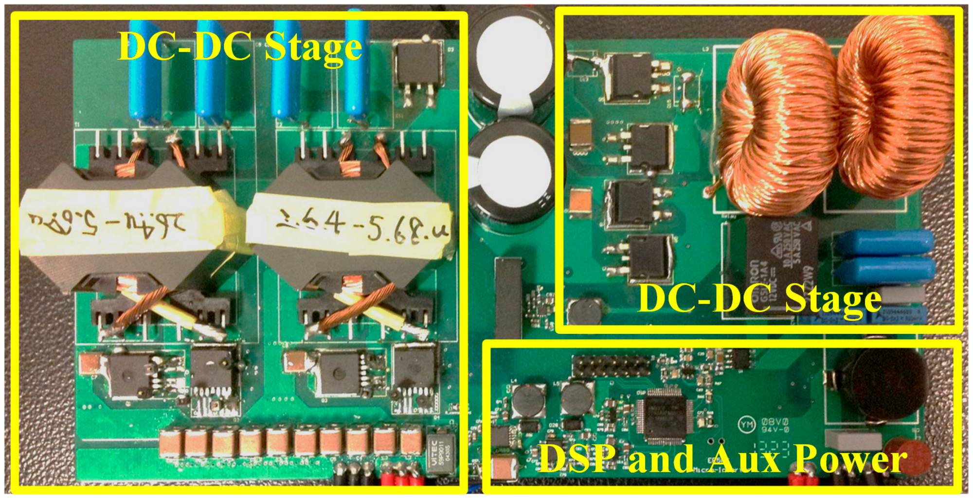
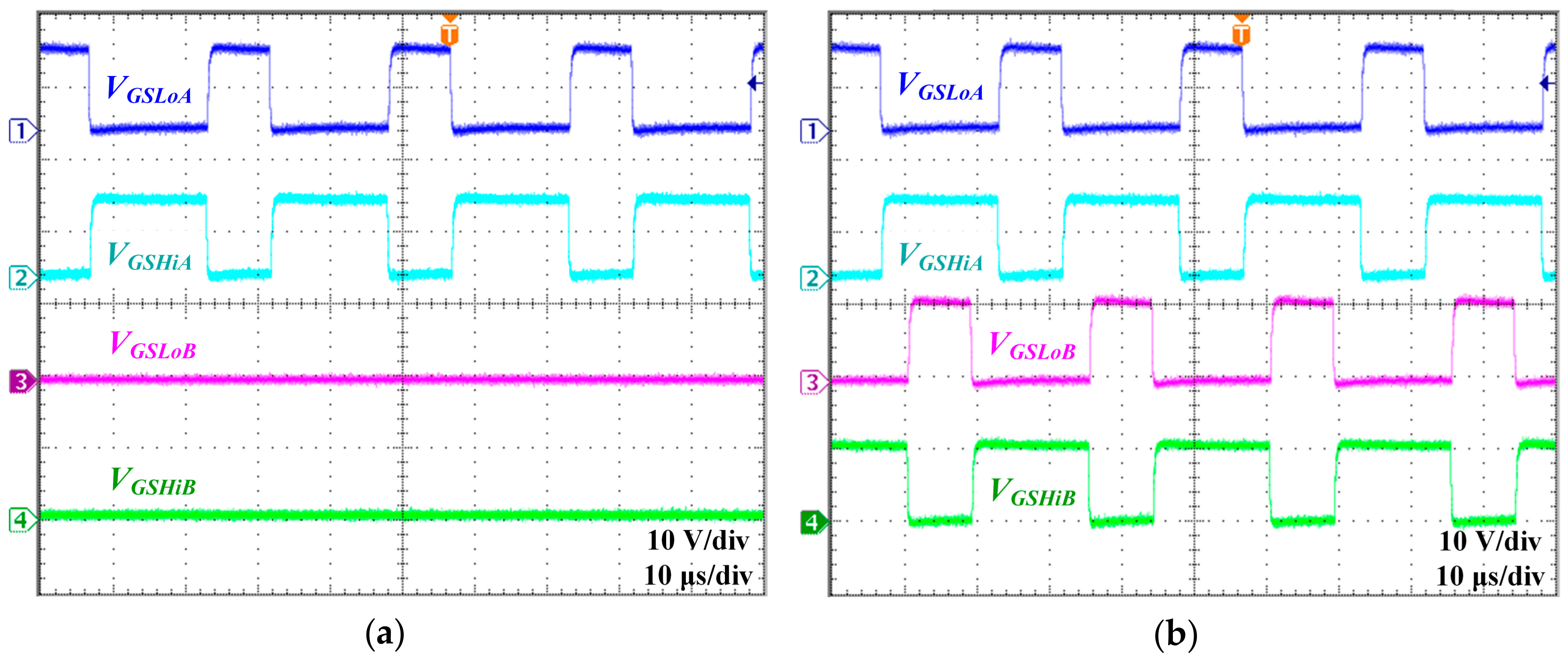
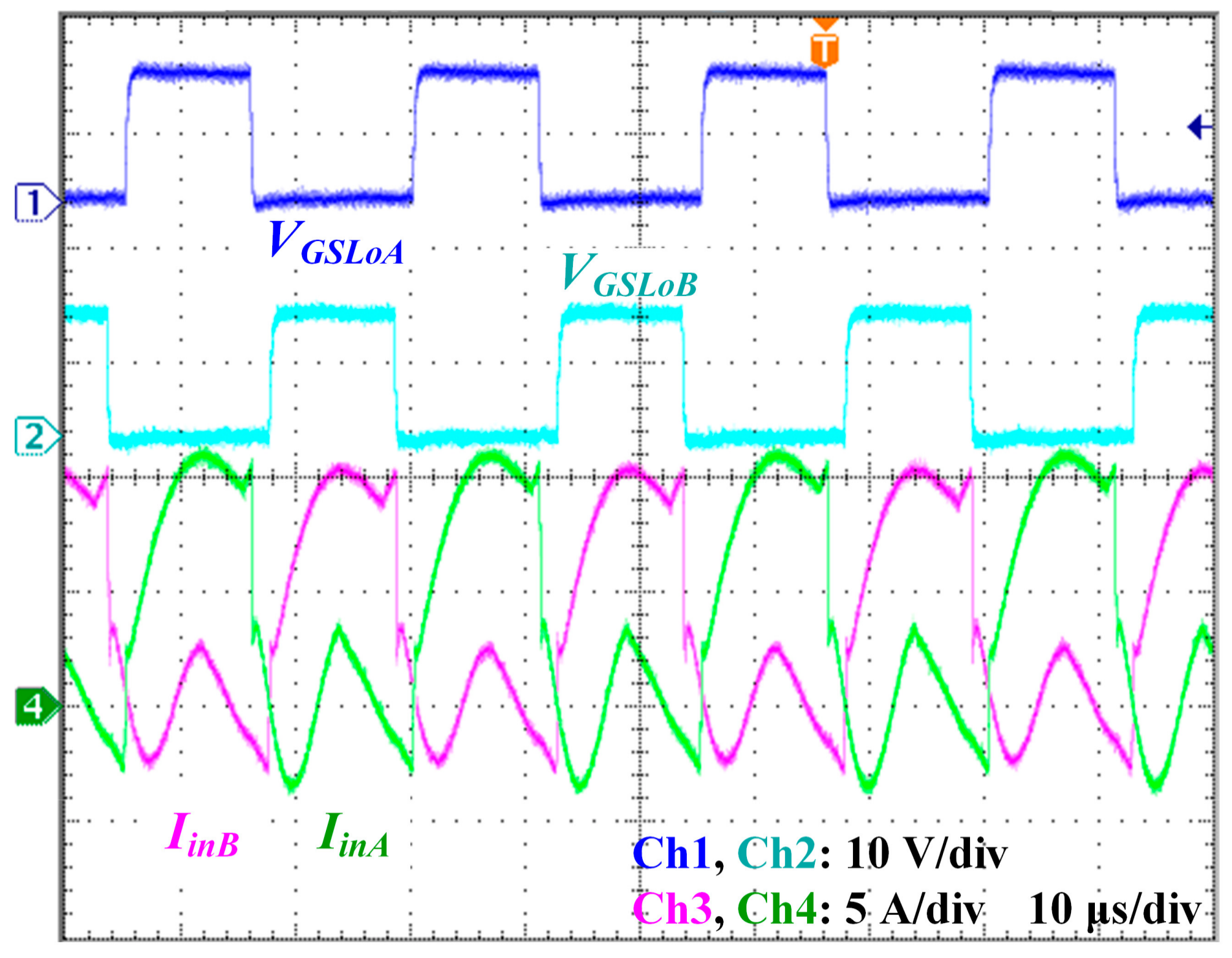
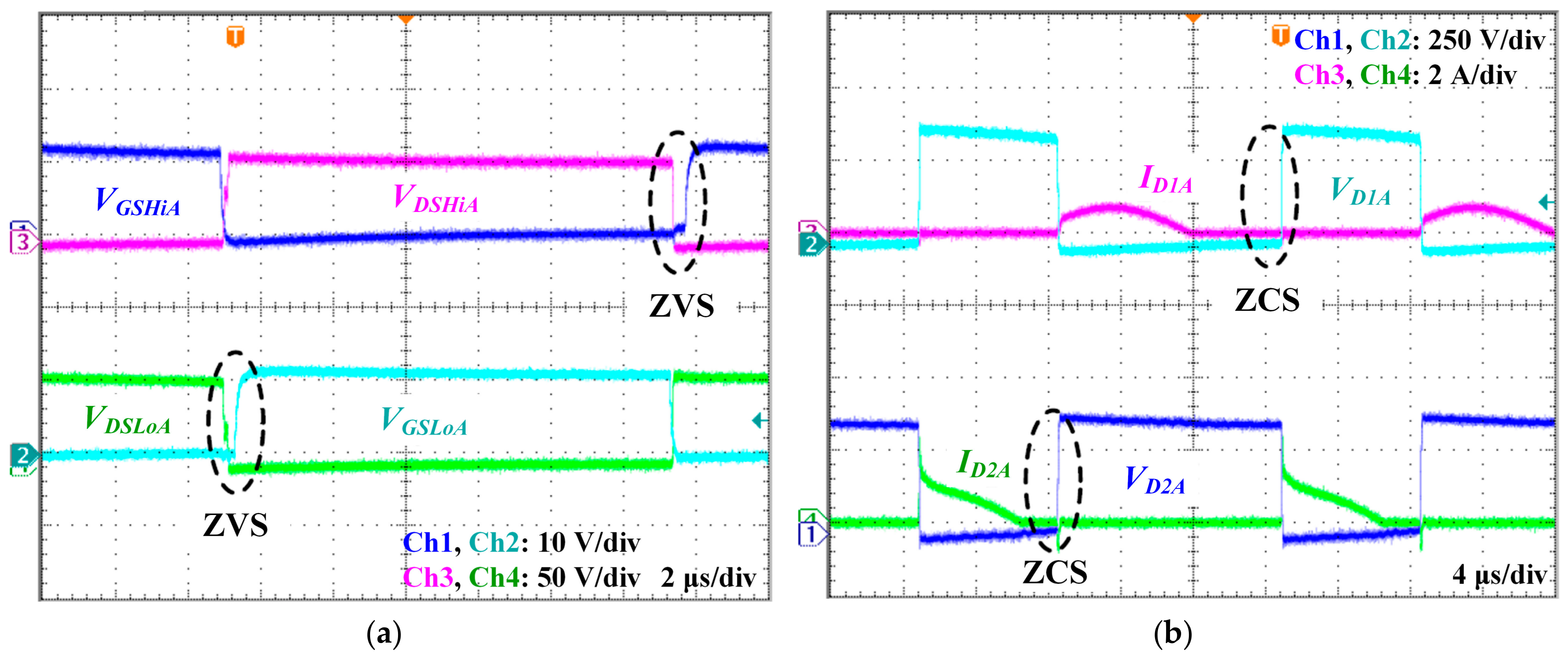
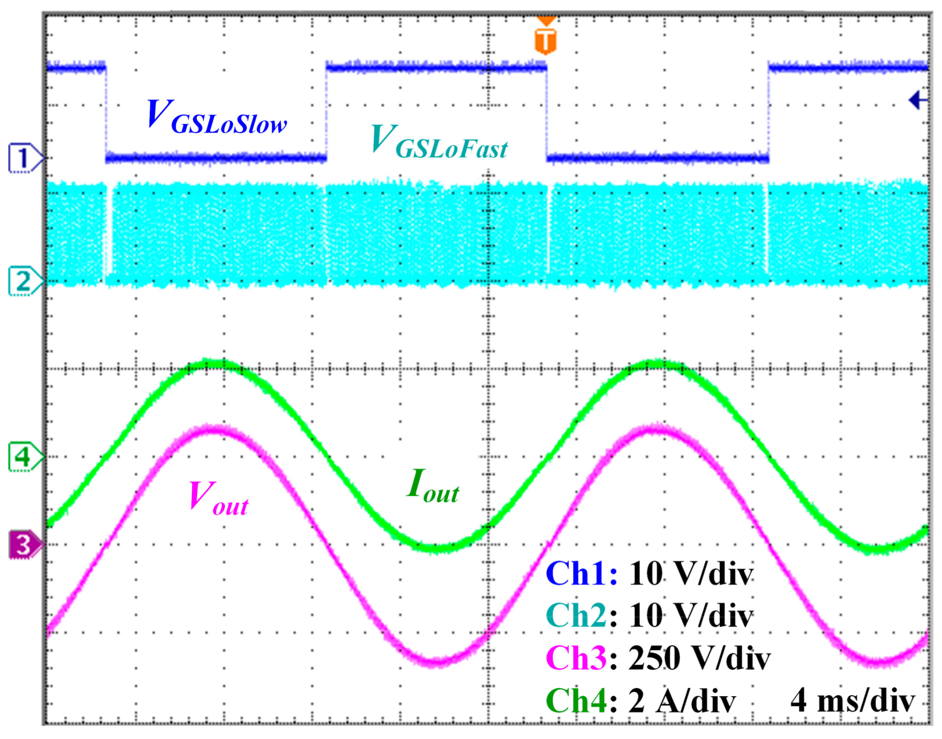
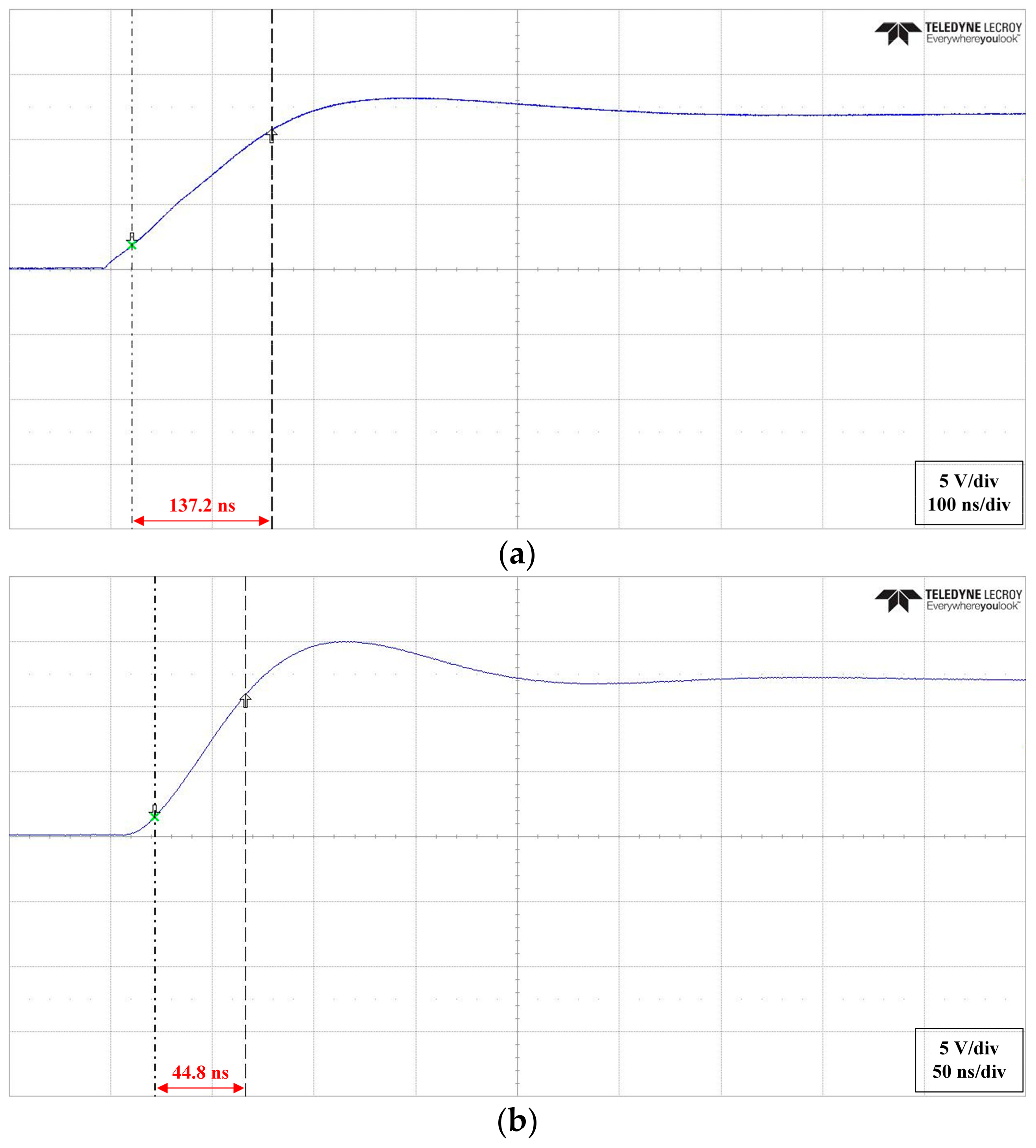
3.2. Experimental Verification

A 500-W microinverter was designed and implemented for both standalone and grid-tied applications. The specifications of the prototype are listed in Table 2. A photograph of the developed prototype system is shown in Figure 13. In the experimental setup, the PV input was a Chroma PV simulator 62150H-1000S.
In the prototype system, several wide band-gap devices were used and tested to improve the efficiency performance. For the interleaved active-clamped forward-flyback converter stage, the CREE SiC diode C3D10060 was used to reduce reverse-recovery loss on the secondary diodes. Infineon CoolMOS 20N60CFD and Transphorm GaN HEMT TPH3006PS were tested and compared in the experiments for high-frequency switches of the inverter stage. Approximately 1% improvement for CEC efficiency can be achieved using GaN HEMT, compared with the results using CoolMOS.
Figure 14 shows the measured gating signals for the DC-DC stage. The converter is operated in single mode at low power levels, as shown in Figure 14a, or interleaved mode, as shown in Figure 14b. The operation mode is changed during operation, depending on the power conditions. The resonant frequencies fr,1 and fr,2 are 66 kHz and 95 kHz, respectively. Figure 15 show the measured resonant current and soft-switching waveforms, which are consistent with the theoretical waveforms shown in Figure 5b. Figure 16 shows the voltage and current waveforms of the power switches, which show that the converter achieves ZVS and ZCS. The efficiency performance of the DC-DC stage, which reaches an efficiency of 97%, is shown in Table 3.
Figure 17 shows the switching waveforms of the dual-frequency full-bridge DC-AC inverter under a 250-W condition, which demonstrates the single-arm switching feature. Table 4 shows the measured efficiency performance under different power conditions. The efficiency reaches 98% at full load.
Table 5 shows the measured overall efficiency of the 500-W microinverter system under an input voltage of 34 V and an output voltage Vo of 240 Vrms. In the grid-tied mode, experimental results showed that the maximum power point was tracked with an accuracy of approximately 99%. The power efficiency of the microinverter system reaches 95% and maintains high efficiency over the full power range.

4. Conclusions

An isolated PV microinverter was studied for standalone and grid-tied applications. An interleaved active-clamp forward-flyback resonant converter was used as the isolated DC-DC converter stage and dual-frequency full-bridge inverter was used as the DC-AC conversion stage was used to achieve high efficiency and reliability of the microinverter. The control algorithm of the microinverter was described for startup, standalone mode, and grid-tied mode. Wide band-gap devices were also used and compared with conventional Si-based devices in the experiments, and GaN switches were selected for the final design. The experimental verifications showed that the prototype system exhibited high efficiency and high MPPT accuracy, reaching 95% for the overall microinverter system.

Acknowledgments

This research was supported by the National Science Council of Taiwan under Grant MOST 105-2218-E-197-002 and MOST 106-2221-E-197-015, and the Basic Science Research Program through the National Research Foundation of Korea funded by the Ministry of Education (2016R1D1A1B03931573).

Author Contributions

Yu-Chen Liu, Ming-Cheng Chen, Chun-Yu Yang, and Huang-Jen Chiu conceived and designed the prototype and experiments; Ming-Cheng Chen and Chun-Yu Yang performed the experiments; Yu-Chen Liu, Ming-Cheng Chen, Chun-Yu Yang, and Katherine A. Kim analyzed the data; Huang-Jen Chiu contributed equipment/materials/analysis tools; Yu-Chen Liu, Ming-Cheng Chen, Katherine A. Kim, and Huang-Jen Chiu wrote the paper.

Conflicts of Interest

The authors declare no conflict of interest. The founding sponsors had no role in the design of the study; in the collection, analyses, or interpretation of data; in the writing of the manuscript; and in the decision to publish the results.

References

  1. Paz, F.; Ordonez, M. High-performance solar MPPT using switching ripple identification based on a lock-in amplifier. IEEE Trans. Ind. Electron. 2016, 63, 3595–3604. [Google Scholar] [CrossRef]
  2. Debnath, D.; Chatterjee, K. Two-stage solar photovoltaic-based stand-alone scheme having battery as energy storage element for rural deployment. IEEE Trans. Ind. Electron. 2015, 62, 4148–4157. [Google Scholar] [CrossRef]
  3. Sahan, B.; Vergara, A.N.; Henze, N.; Engler, A.; Zacharias, P. A single-stage PV module integrated converter based on a low-power current-source inverter. IEEE Trans. Ind. Electron. 2008, 55, 2602–2609. [Google Scholar] [CrossRef]
  4. Suntio, T.; Leppaaho, J.; Huusari, J.; Nousiainen, L. Issues on Solar-Generator Interfacing With Current-Fed MPP-Tracking Converters. IEEE Trans. Power Electron. 2010, 25, 2409–2419. [Google Scholar] [CrossRef]
  5. Huusari, J.; Suntio, T. Dynamic Properties of Current-Fed Quadratic Full-Bridge Buck Converter for Distributed Photovoltaic MPP-Tracking Systems. IEEE Trans. Power Electron. 2012, 27, 4681–4689. [Google Scholar] [CrossRef]
  6. Femia, N.; Lisi, G.; Petrone, G.; Spagnuolo, G.; Vitelli, M. Distributed maximum power point tracking of photovoltaic arrays: Novel approach and system analysis. IEEE Trans. Ind. Electron. 2008, 55, 2610–2621. [Google Scholar] [CrossRef]
  7. Khan, O.; Xiao, W.; Zeineldin, H.H. Gallium-nitride-based submodule integrated converters for high-efficiency distributed maximum power point tracking PV applications. IEEE Trans. Ind. Electron. 2016, 63, 966–975. [Google Scholar] [CrossRef]
  8. Vázquez, M.J.V.; Márquez, J.M.A.; Manzano, F.S. A methodology for optimizing stand-alone PV-system size using parallel-connected DC/DC converters. IEEE Trans. Ind. Electron. 2008, 55, 2664–2673. [Google Scholar] [CrossRef]
  9. Killi, M.; Samanta, S. An adaptive voltage-sensor-based MPPT for photovoltaic systems with SEPIC converter including steady-state and drift analysis. IEEE Trans. Ind. Electron. 2015, 62, 7609–7619. [Google Scholar] [CrossRef]
  10. Xiao, W.; Ozog, N.; Dunford, W.G. Topology study of photovoltaic interface for maximum power point tracking. IEEE Trans. Ind. Electron. 2007, 54, 1696–1704. [Google Scholar] [CrossRef]
  11. Lin, F.J.; Chiang, H.C.; Chang, J.K. Modeling and Controller Design of PV Micro Inverter without Using Electrolytic Capacitors and Input Current Sensors. Energies 2016, 9, 993. [Google Scholar] [CrossRef]
  12. Nousiainen, L.; Puukko, J.; Mäki, A.; Messo, T.; Huusari, J.; Jokipii, J.; Viinamäki, J.; Lobera, D.T.; Valkealahti, S.; Suntio, T. Photovoltaic Generator as an Input Source for Power Electronic Converters. IEEE Trans. Power Electron. 2013, 28, 3028–3038. [Google Scholar] [CrossRef]
  13. Suntio, T.; Messo, T.; Aapro, A.; Kivimäki, J.; Kuperman, A. Review of PV Generator as an Input Source for Power Electronic Converters. Energies 2017, 10, 1076. [Google Scholar] [CrossRef]
  14. Zapata, J.W.; Kouro, S.; Carrasco, G.; Renaudineau, H. Step-Up Partial Power DC-DC Converters for Two-Stage PV Systems with Interleaved Current Performance. Energies 2018, 11, 357. [Google Scholar] [CrossRef]
  15. Suntio, T.; Messo, T.; Puukko, J. Power Electronic Converters: Dynamics and Control in Conventional and Renewable Energy Applications; Wiley: Weinheim, Germany, 2017; ISBN 978-3-527-34022-4. [Google Scholar]
  16. Park, J.H.; Ahn, J.Y.; Cho, B.H.; Yu, G.J. Dual-module-based maximum power point tracking control of photovoltaic systems. IEEE Trans. Power Electron. 2006, 53, 1036–1047. [Google Scholar] [CrossRef]
  17. Sree, K.R.; Rathore, A.K. Hybrid modulated extended secondary universal current-fed ZVS converter for wide voltage range: Analysis, design, and experimental results. IEEE Trans. Power Electron. 2015, 62, 4471–4480. [Google Scholar] [CrossRef]
  18. Mutoh, N.; Inoue, T. A control method to charge series-connected ultraelectric double-layer capacitors suitable for photovoltaic generation systems combining MPPT control method. IEEE Trans. Power Electron. 2007, 54, 374–383. [Google Scholar] [CrossRef]
  19. Chakraborty, C.; Iu, H.H.C.; Lu, D.D.C. Power converters, control, and energy management for distributed generation. IEEE Trans. Power Electron. 2015, 62, 4466–4470. [Google Scholar] [CrossRef]
  20. Huang, Z.; Recht, F.; Wu, Y. PCB Layout and Probing for GaN Power Switches; Application Note AN-0003, Rev. 2; Transphorm Inc.: Goleta, CA, USA, 2015. [Google Scholar]
  21. Kolar, J.; Krismer, F.; Lobsiger, Y.; Muhlethaler, J.; Nussbaumer, T.; Minibock, J. Extreme efficiency power electronics. In Proceedings of the International Conference on Integrated Power Electronics Systems (CIPS), Nuremberg, Germany, 6–8 March 2012; pp. 1–22. [Google Scholar]
  22. Viinamäki, J.; Kuperman, A.; Suntio, T. Grid-Forming-Mode Operation of Boost-Power-Stage Converter in PV-Generator-Interfacing Applications. Energies 2017, 10, 1033. [Google Scholar] [CrossRef]
Figure 1. Power converter system diagram of an isolated photovoltaic (PV) microinverter system.
Energies 11 00569 g001
Figure 2. Block diagram of the proposed microinverter system in standalone and on grid mode. MPPT, maximum power point tracking.
Energies 11 00569 g002
Figure 3. Circuit schematic of the DC-DC and DC-AC stages for the proposed microinverter system.
Energies 11 00569 g003
Figure 4. Theoretical waveforms of the dual-frequency full-bridge inverter.
Energies 11 00569 g004
Figure 5. (a) Circuit schematic and (b) theoretical waveforms of the active-clamp forward-flyback resonant converter.
Energies 11 00569 g005
Figure 6. Switching states of the active-clamped forward-flyback resonant converter.
Energies 11 00569 g006
Figure 7. Detailed resonant waveform of the converter.
Energies 11 00569 g007
Figure 8. Control flowchart of the proposed microinverter system.
Energies 11 00569 g008
Figure 9. Control block diagram for the DC-DC stage and inverter in standalone mode. ADC, analog to digital converter; OVP, over voltage protection; UVP, under voltage protection; 2P2Z, 2 pole 2 zero; EN, interleaved enable signal; PWM, pulse-width modulation; NCO, numerically controlled oscillator; PR, proportional-resonant.
Energies 11 00569 g009
Figure 10. Control block diagram for the DC-DC stage and inverter in grid-tied mode.
Energies 11 00569 g010
Figure 11. Switching waveforms of the (a) CoolMOS 20N60CFD and (b) GaN HEMT TPH3006PS.
Energies 11 00569 g011
Figure 12. Gate driver circuit for the GaN HEMT power switches.
Energies 11 00569 g012
Figure 13. Photograph of the 500-W Microinverter experimental prototype.
Energies 11 00569 g013
Figure 14. Waveforms of the gating signals for the DC-DC stage in (a) single and (b) interleaved modes.
Energies 11 00569 g014
Figure 15. Gate and resonant current waveforms of the resonant converter.
Energies 11 00569 g015
Figure 16. Waveforms of the switches showing (a) zero-voltage switching (ZVS) and (b) zero-current switching (ZCS) achieved in the circuit.
Energies 11 00569 g016
Figure 17. Measured waveforms for the inverter stage of the microinverter.
Energies 11 00569 g017
Table 1. Parameter of GAN HEMT and COOLMOS Devices.
DeviceOn-Resistance (Ω)Gate-Charge (nC)FOM
GaN HEMT TPH3006PS0.156.20.93
CoolMOS 20N60CFD0.199518.05
Table 2. Circuit Specifications for the microinverter experimental prototype.
ParameterSymbolSpecification
Input voltageVin18–40 V
Output voltageVo240 Vrms
Output currentIo2.1 Arms (rated)
Efficiencyŋ≥0.95 (at 375 W)
Voltage THDTHDv≤5% (at nominal output)
Table 3. Experimental results for the DC-DC stage.
ModePo (W)Efficiency (%)
single10097.10
interleaved25097.25
interleaved37597.10
interleaved50096.50
Table 4. Experimental results for the dual-frequency full-bridge inverter stage.
Vbus (V)Vo (Vrms)Po (W)Efficiency (%)
38024010096.65
38024025097.80
38024037598.00
38024050098.15
Table 5. Experimental results for the full 500-W microinverter system.
Vpv (V)Vo (Vrms)Po (W)Efficiency (%)
3424010094.15
3424025095.25
3424037595.17
3424050094.70

