Secure Protocol and IP Core for Configuration of Networking Hardware IPs in the Smart Grid

 , , and
Abstract
:1. Introduction
- Offset Codebook Mode (OCB) is a very fast mode, it produces low overhead on the encryption algorithm used, but it has the drawback of using patented techniques.
- Counter with CBC-MAC (CCM), is considerably slower than OCB; however, the decrease in performance is acceptable considered that there is no need to pay for patents.
- Galois Counter Mode (GCM) can take full advantage of parallel processing, thus, reducing the overhead. Therefore, it is more efficient than OCB and does not have the drawback of patents.
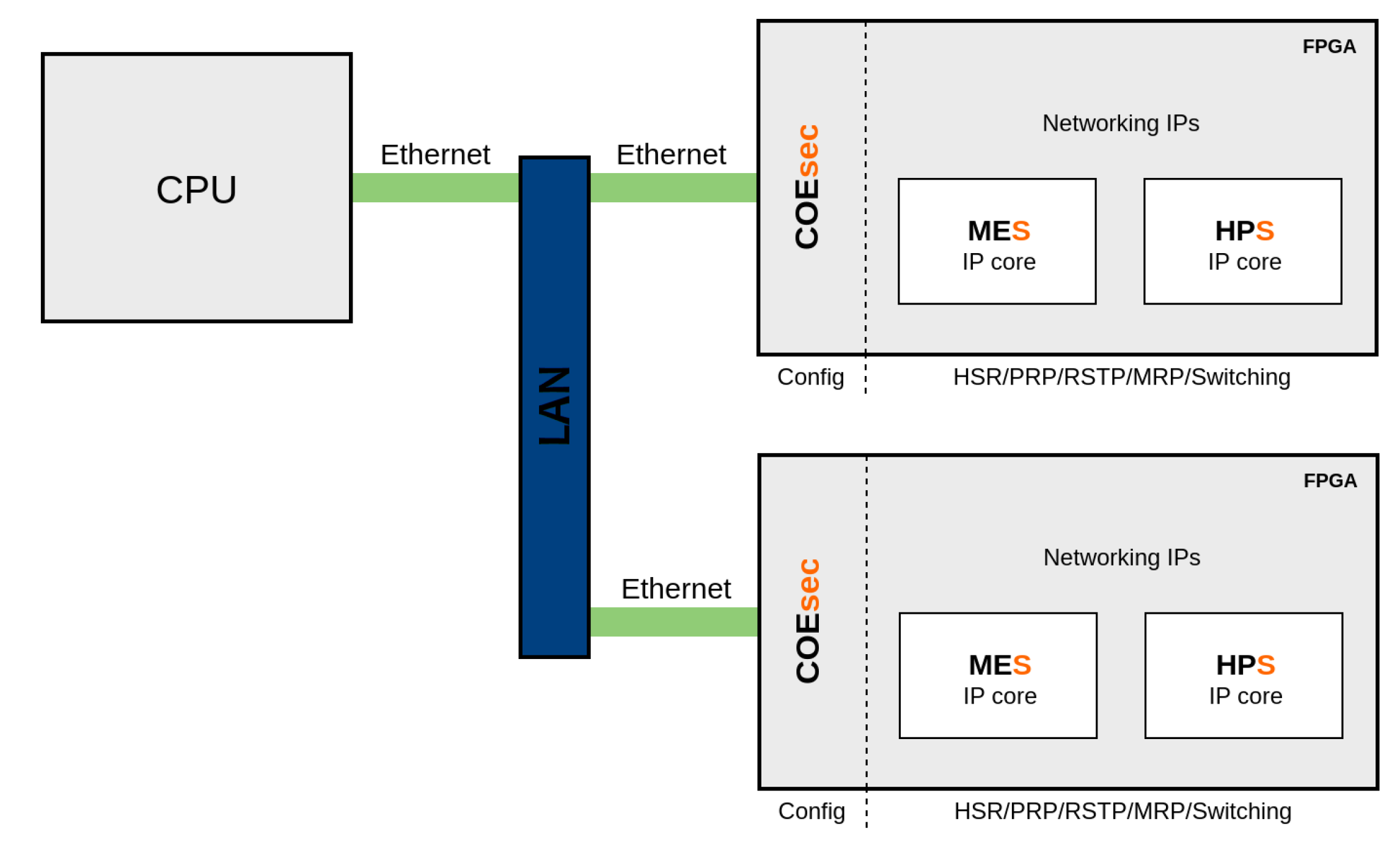
2. Protocol Definition
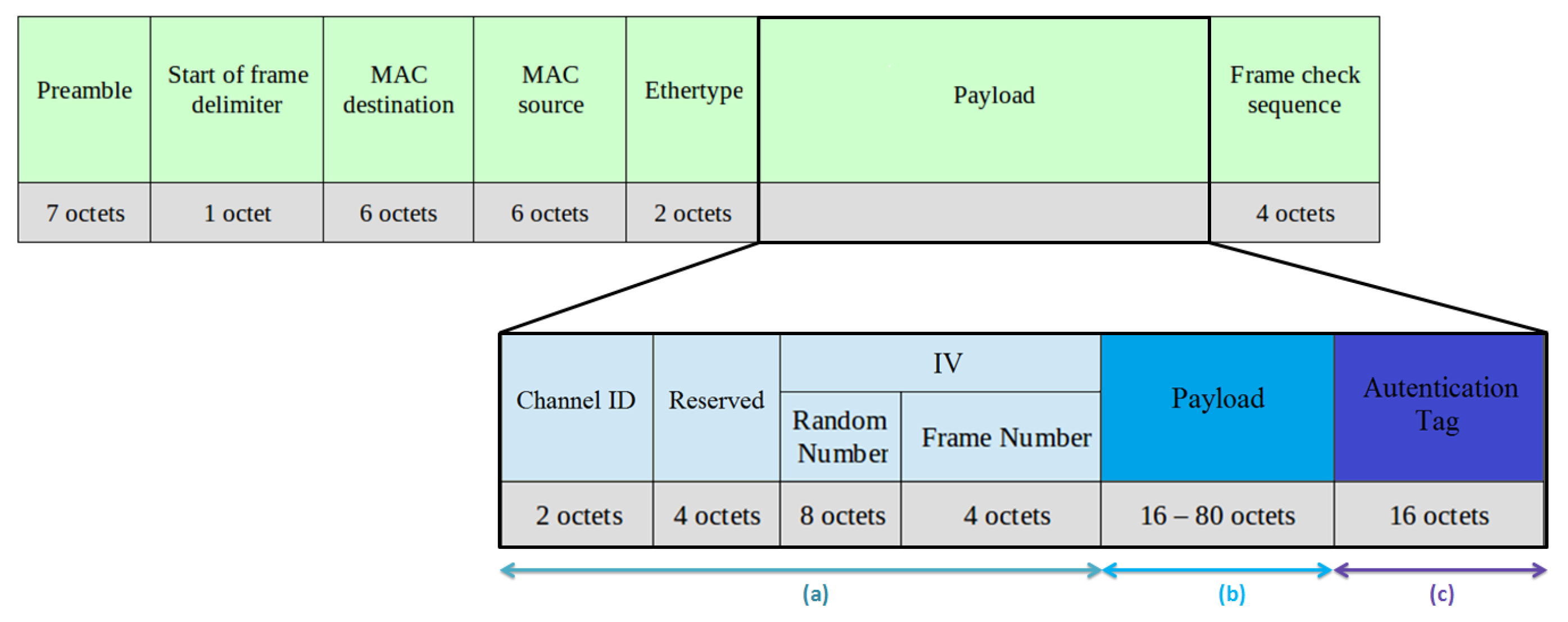
- Channel ID: each COEsec communication is identified by a channel ID. This field is used to associate the sender/receiver to its secret key that is used to encrypt/decrypt and authenticate the messages. It is two bytes long. This field is stored in an FPGA register.
- Reserved: it is a four-bytes long field reserved for future use. All of them must be set to zero.
- IV: it is a twelve-bytes long initialization vector used for the encryption/decryption of the messages and it is needed to provide randomness to the messages and to ensure confidentiality. It is divided in two sub-fields: a random number and a frame number.
- -
- Random Number: it is an eight-bytes long random number that allows the encryption algorithm to achieve semantic security and prevents an attacker from inferring relationships between segments of different encrypted messages.
- -
- Frame Number: it is a four-bytes long frame number that identifies each couple of messages (i.e., petition and response) exchanged between a sender and a receiver and, it is associated to a certain channel ID. The sender should increase the frame number with each new frame. In case of the sender using an invalid frame number, an automatic response message will be generated, the response contains the same frame number that the petition received and whose payload will contain the valid frame number expected to receive for that channel ID. When the maximum frame number value is reached, the value should be reset to zero.
- Payload: it contains the encrypted configuration commands (both reading and writing operations) and their respective responses. There are two types of COE commands: read and write.To read a register, it is necessary to provide the address associated with the register to be read and an operation identifier. The command would be as follows:where “x” is the memory address to be read (16 bits) and R is the identifier of the command (R-Read).To write a register, it is necessary to provide the address associated with the register to be written, the data to be written to the register and an operation identifier. The command would be as follows:where “x” is the memory address to be written (16 bits), “d” is the data to write (32 bits) and W is the identifier of the command (W-Write).
- Authentication Tag: in order to prevent an attacker from modifying the messages, an authentication tag is used (16 bytes long). This tag has been generated using a Hash function which assures that if any of the bits of the authenticated fields changes, the tag will take a different value. The authenticated fields are: Channel ID, Reserved, IV and Payload, as well as, the Ethernet header (MAC destination, MAC source and Ethertype).
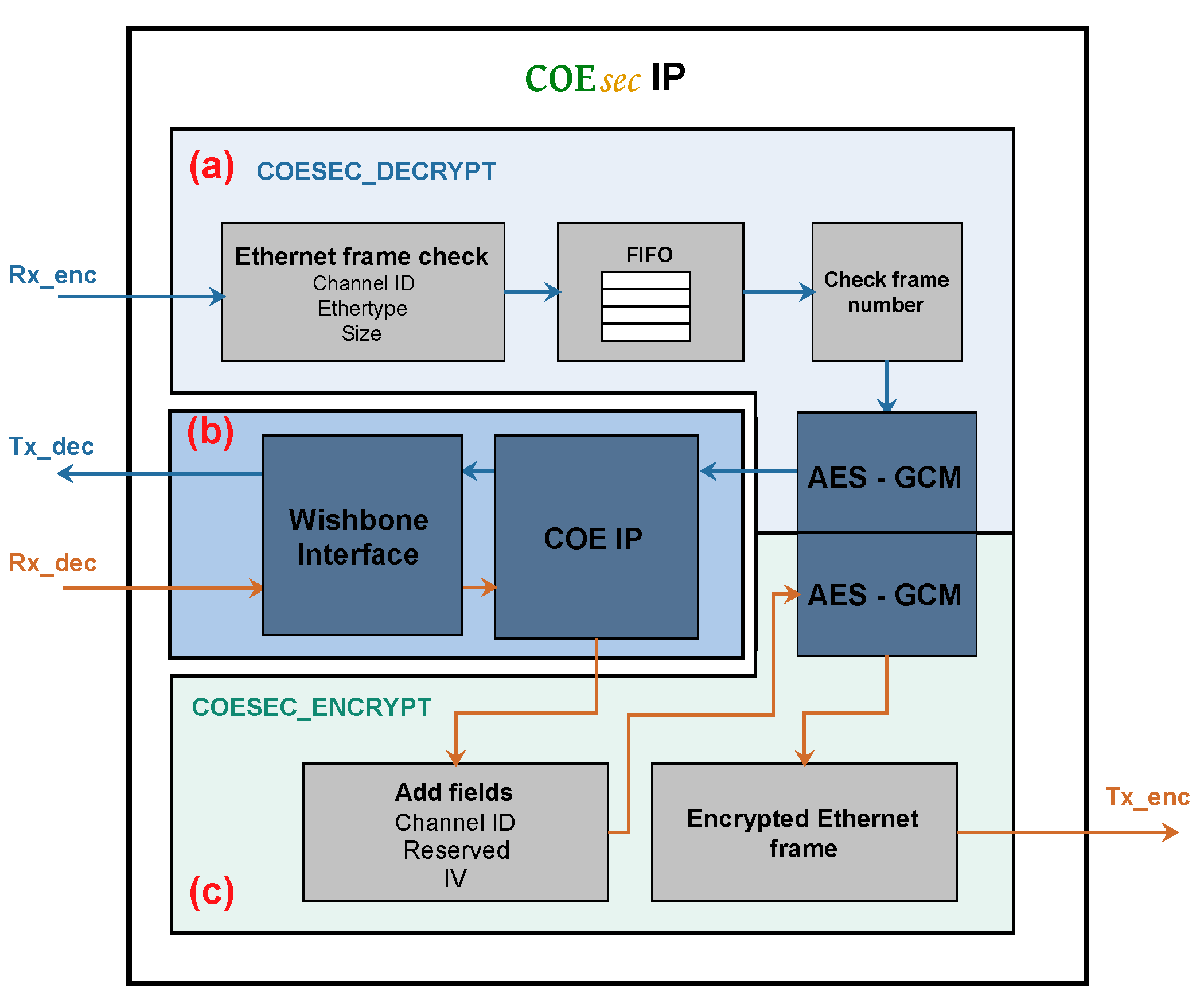
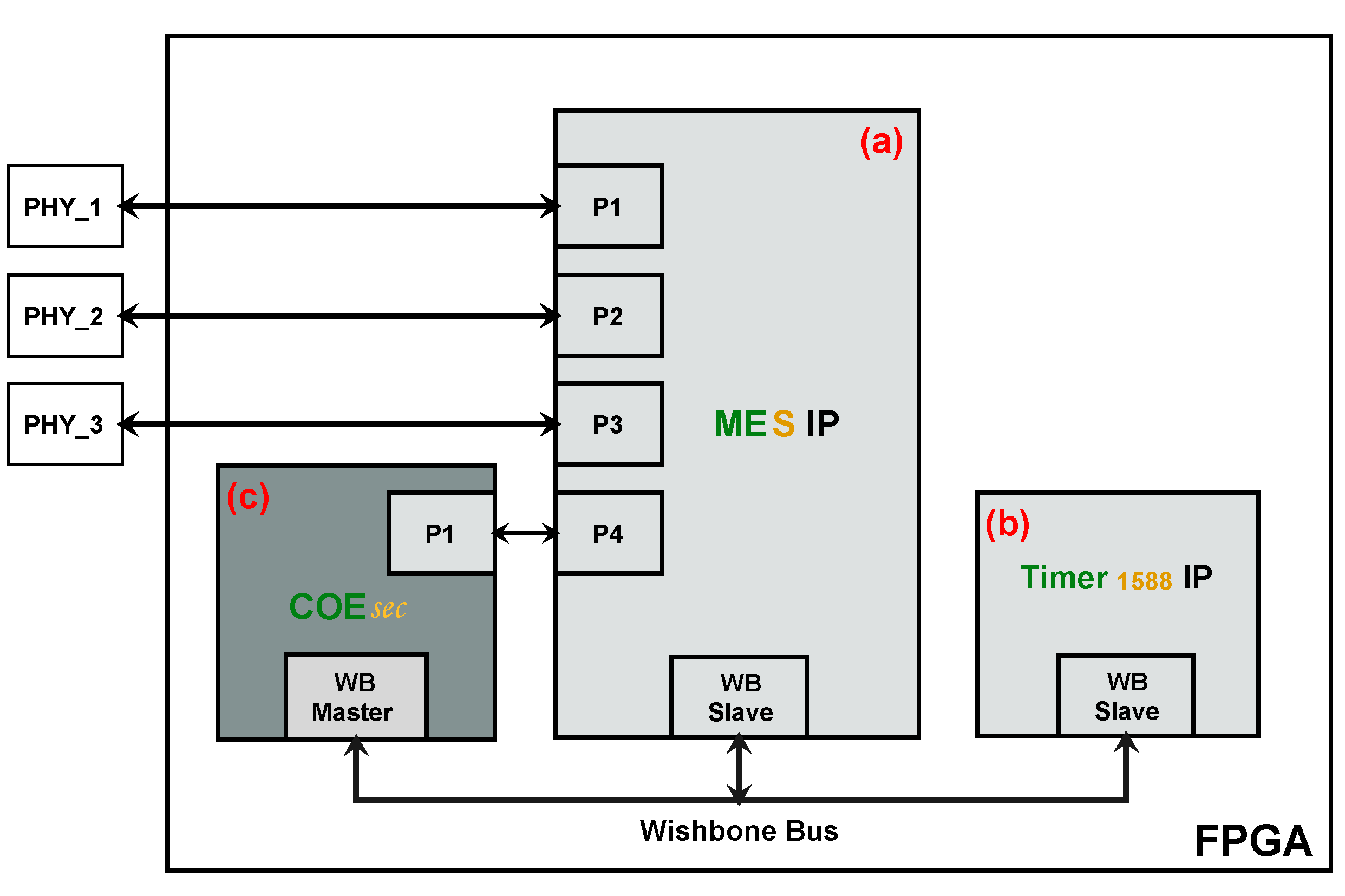
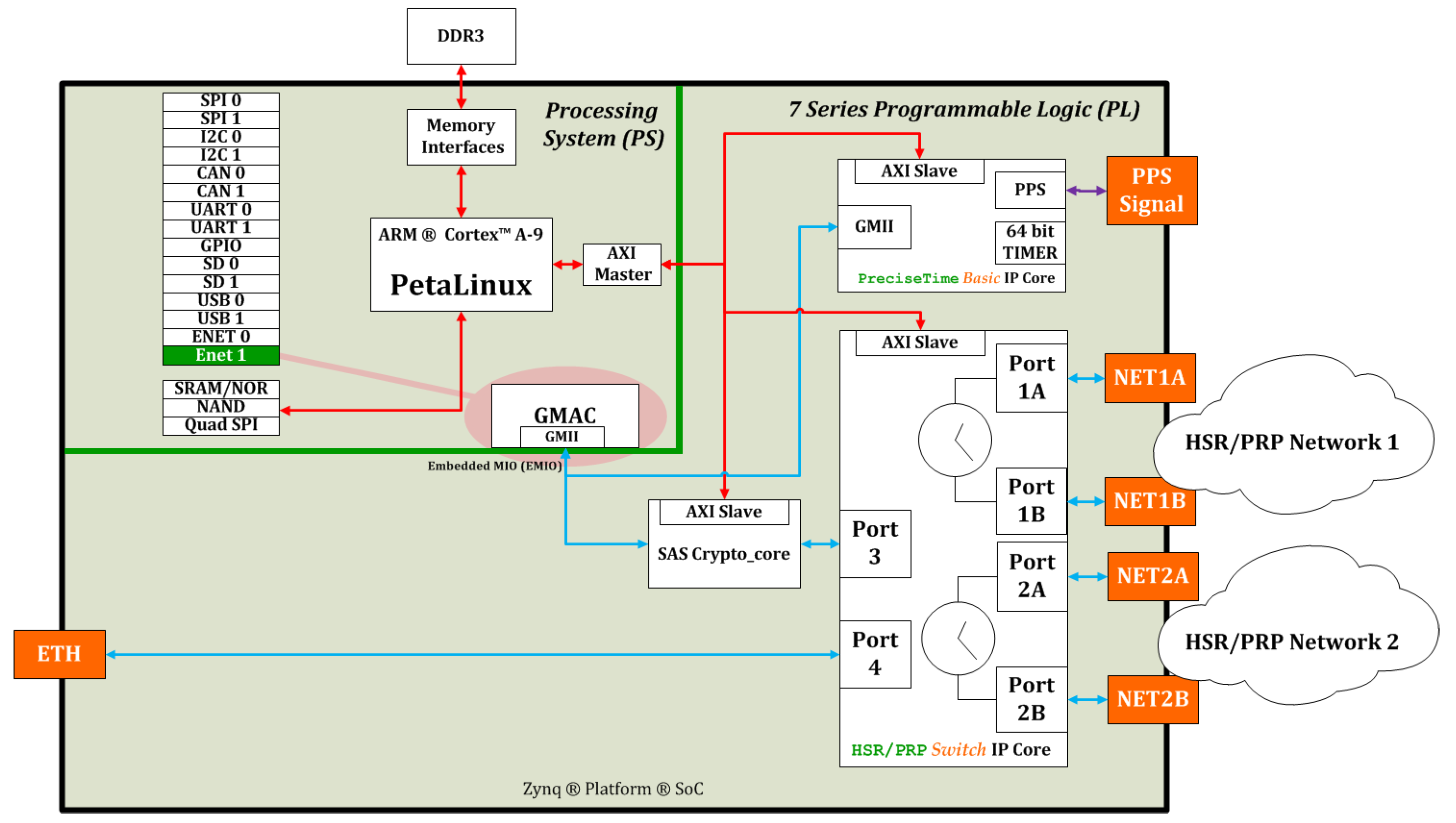
3. Implementation
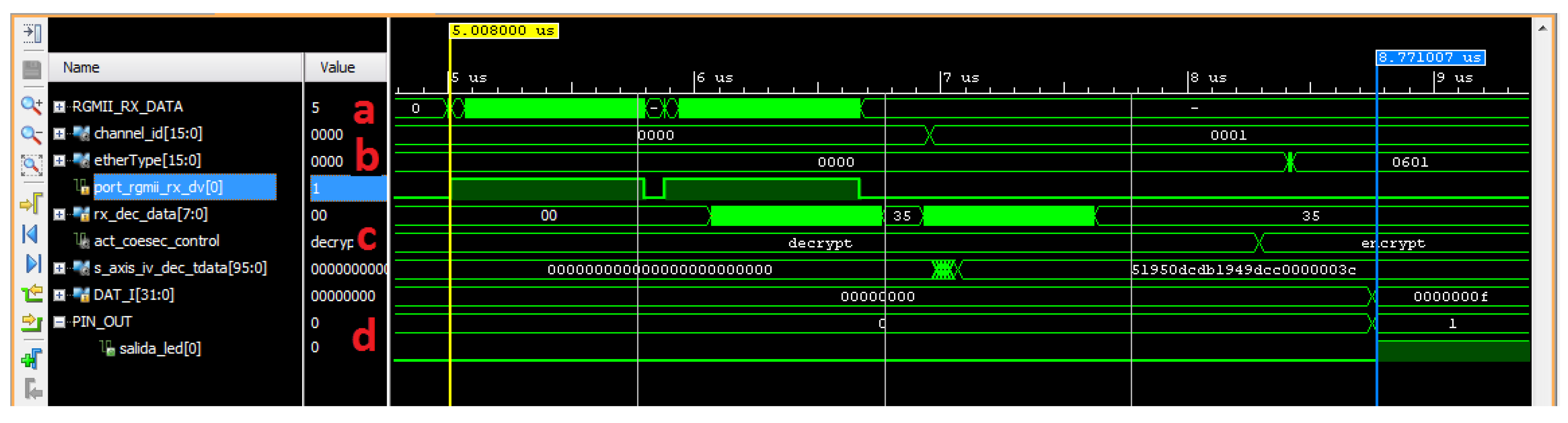
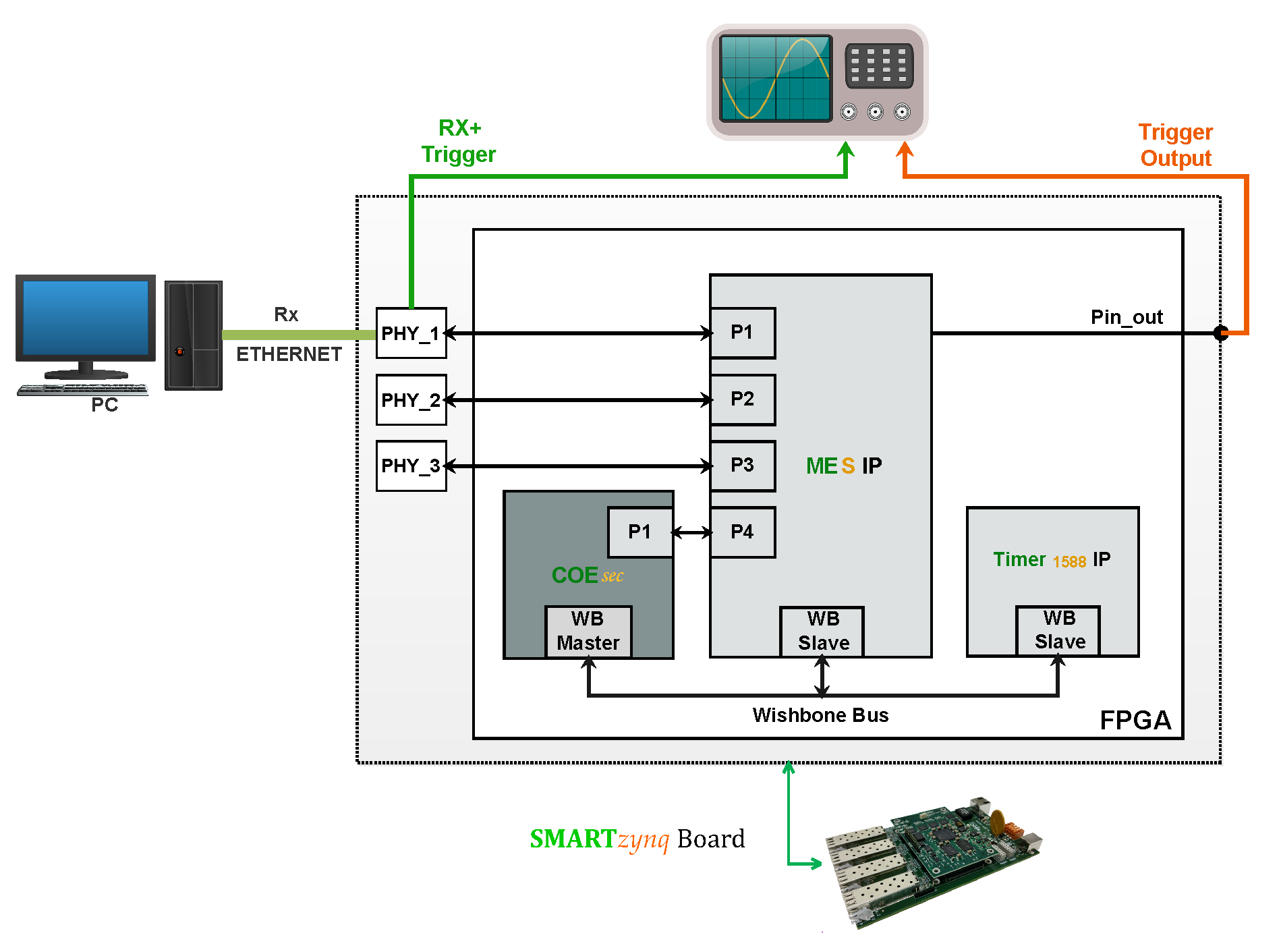
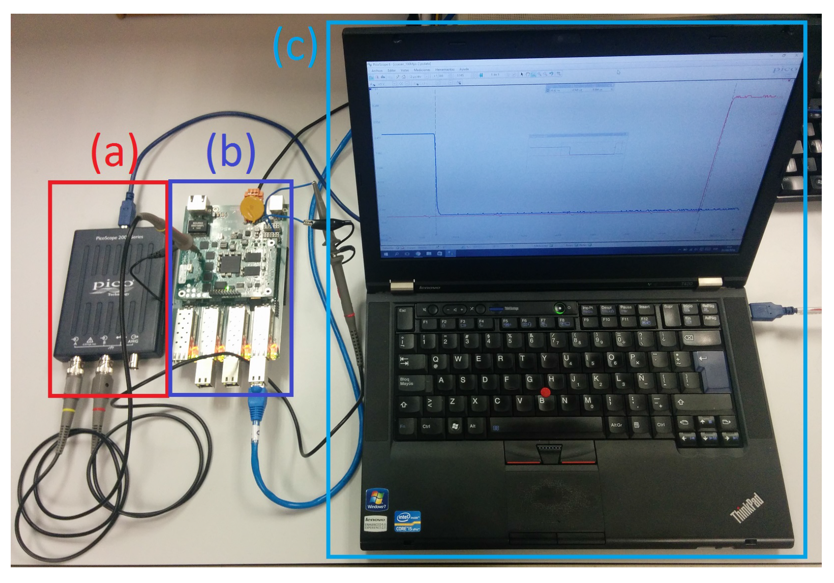
4. Validation
5. Comparison with Existing Schemes
6. Conclusions
Acknowledgments
Author Contributions
Conflicts of Interest
References
- Jiang, X. High Availability Seamless Ring Protocol Implementation in FPGA. Master’s Thesis, Swiss Federal Institute of Technology (Zurich), Zurich, Switzerland, 2009. [Google Scholar]
- Araujo, J.A. Alta Fiabilidad Por Redundancia en Redes Industriales Sobre Ethernet. Master’s Thesis, Faculty od Engineering, University of the Basque Country, Vizcaya, Spain, 2011. [Google Scholar]
- A System Solution for IEDs Based on IEC 61850; Analog Devices: Norwood, MA, USA, 2013.
- Reyrolle 7SR110 & 7SR120 Argus. SIEMENS: Munich, Germany, 2017. Available online: http://w3.siemens.com/smartgrid/global/en/products-systems-solutions/Protection/overcurrent-feeder-protection/Pages/7SR110-7SR120.aspx (accessed on 22 January 2018).
- IEC 61850 Substation Control and Automation Devices; Arteche Group: Mungia, Spain, 2017.
- IEC 61850 on HSR/PRP Communication Modules from SoC-e; SystemCORP Embedded Technology: Beckenham, Australia, 2017.
- Kashyap, H.J. Secure Dynamic Reconfiguration of FPGAs. ACM Trans. Reconfig. Technol. Syst. 2014, 7. [Google Scholar] [CrossRef]
- Devic, F.; Torres, L.; Crenne, J.; Badrignans, B.; Benoît, P. SecURe DPR: Secure update preventing replay attacks for dynamic partial reconfiguration. In Proceedings of the International Conference on Field Programmable Logic and Applications, (FPL ), Oslo, Norway, 29–31 August 2012; pp. 57–62. [Google Scholar]
- Vliegen, J.; Mentcns, N.; Verbauwhede, I. A single-chip solution for the secure remote configuration of FPGAs using bitstream compression. In Proceedings of the International Conference on Reconfigurable Computing and FPGAs, (ReConFig), Cancun, Mexico, 9–11 December 2013. [Google Scholar]
- Castillo, J.; Huerta, P.; Martínez, J.I. Secure IP downloading for SRAM FPGAs. Microprocess. Microsyst. 2007, 31, 77–86. [Google Scholar] [CrossRef]
- Kevin, P. Slammer Worm Crashed Ohio Nuke Plant Network. SecurityFocus, Register 2003, 20, 1–4. Available online: http://www.securityfocus.com/news/6767 (accessed on 23 January 2018).
- Kushner, D. The Real Story of Stuxnet. IEEE Spectr. 2013, 50, 48–53. [Google Scholar] [CrossRef]
- Fairley, P. Cybersecurity at U.S. Utilities Due For an Upgrade. IEEE Spectr. 2016, 53, 11–13. [Google Scholar]
- North American Electric Reliability Council. SQL Slammer Worm Lessons Learned for Consideration by the Electricity Sector; Technical Report; NERC: Atlanta, Georgia, 2003. [Google Scholar]
- Liu, J.; Xiao, Y.; Member, S.; Li, S.; Liang, W.; Chen, C.L.P. Cyber Security and Privacy Issues in Smart Grids. IEEE Commun. Surv. Tutor. 2012, 14, 981–997. [Google Scholar] [CrossRef]
- Ericsson, G. Cyber Security and Power System Communication—Essential Parts of a Smart Grid Infrastructure. IEEE Trans. Power Deliv. 2010, 25, 1501–1507. [Google Scholar] [CrossRef]
- Cleveland, F. IEC TC57 WG15: IEC 62351 Security Standards for the Power System Information Infrastructure; White Paper ver 14; International Electrotechnical Commission: Geneva, Switzerland, 2012. [Google Scholar]
- International Electrotechnical Commission. IEC-TS 62351-6 ed1.0 Power Systems Management and Associated Information Exchange—Data and Communication Security—Part 6. Security for IEC 61850; IEC: Geneva, Switzerland, 2007. [Google Scholar]
- International Electrotechnical Commission. IEC 61850-1 ed2.0 Communication Networks and Systems for Power Utility Automation—Part 1. Introduction and Overview; IEC: Geneva, Switzerland, 2013. [Google Scholar]
- Fuloria, S.; Anderson, R.; McGrath, K.; Hansen, K.; Alvarez, F. The Protection of Substation Communications. In Proceedings of the SCADA Security Scientific Symposium, Miami, FL, USA, 17–18 January 2010. [Google Scholar]
- Fries, S.; Falk, R. Security Considerations for Multicast Communication in Power Systems. Int. J. Adv. Secur. 2013, 6, 111–121. [Google Scholar]
- Dworkin, M. Recommendation for Block Cipher Modes of Operation Methods and Techniques, 2001. Available online: https://nvlpubs.nist.gov/nistpubs/SpecialPublications/NIST.SP.800-38G.pdf (accessed on 22 January 2018).
- Montes, M.; Penazzi, D. Dos nuevos algoritmos de cifrado autenticado. Silver y CPFB. Workshop Segur. Inform. 2014, 2014, 31–45. [Google Scholar]
- Usselmann, R. Advanced Encryption Standard/Rijndael IP Core. 2002. Available online: https://opencores.org/project,aescore,downloads (accessed on 22 January 2018).
- SoC-e. MES, Managed Ethernet Switch IP Core. 2016. Available online: http://soc-e.com/mes-managed-ethernet-switch-ip-core/ (accessed on 22 January 2018).
- WISHBONE System-on-Chip (SoC) Interconnection Architecturefor Portable IP Cores. Technical Report, 2002. OPENCORES.ORG. Available online: https://cdn.opencores.org/downloads/wbspec_b3.pdf (accessed on 22 January 2018).
- SoC-e. SMARTzynq Module: 5 Port Gigabit Ethernet Industrial Embedded Switch Module. 2016. Available online: http://soc-e.com/products/smart-zynq-module/ (accessed on 22 January 2018).
- Mishra, V.; Chen, Q.; Zervas, G. REoN: A Protocol for Reliable Software-Defined FPGA Partial Reconfiguration over Network. In Proceedings of the International Conference on Reconfigurable Computing and FPGAs, (ReConFig), Cancun, Mexico, 30 November–2 December 2016. [Google Scholar]


| Resources | COE without Security | COEsec with Security | Available | Percent COE without Security | Percent COEsec with Security |
|---|---|---|---|---|---|
| Slice Registers | 1215 | 4138 | 106,400 | 1.14 % | 3.89 |
| Slice LUT | 1318 | 4748 | 53,200 | 2.48 % | 8.92 |
| Block RAMs | 0.5 | 5.5 | 140 | 0.36 % | 3.93 |
| Resources | COEsec | Switching Infrastructure IPs | Full Design | Percent COEsec | Percent Switching Infrastructure IPs |
|---|---|---|---|---|---|
| Slice Registers | 4138 | 9522 | 13,660 | 30.29 % | 69.71 |
| Slice LUT | 4748 | 7942 | 12,690 | 37.41 % | 62.59 |
| Block RAMs | 5.5 | 31 | 36.5 | 15.06 % | 84.94 |
| Type | 10 Mbps | 100 Mbps | 1 Gbps |
|---|---|---|---|
| Reading | s | s | s |
| Writing | s | s | s |
| Link | Parameter | Typ | Units |
|---|---|---|---|
| 1000 BASE-T | Star of Packet to RX_CTL Asserted | 236 | ns |
| 100 BASE-T | Star of Packet to RX_CTL Asserted | 357 | ns |
| 10 BASE-T | Star of Packet to RX_CTL Asserted | 2.18 | s |
| Rates | Frame Writing | ||
|---|---|---|---|
| Simulation + PHY-Latency (s) | Measurement (s) | Percent Deviation (%) | |
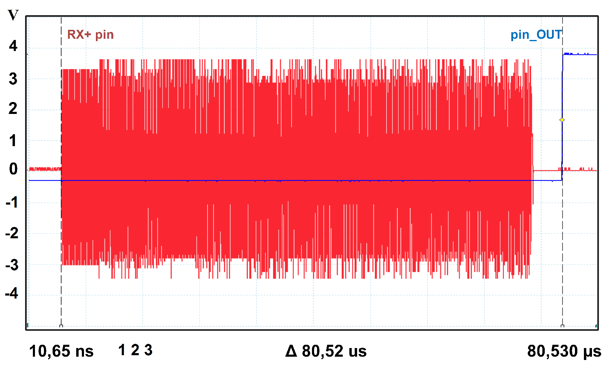
| 10 Mbps | 80.376 | 80.520 | 0.18 |
| 100 Mbps | 10.509 | 10.650 | 1.34 |
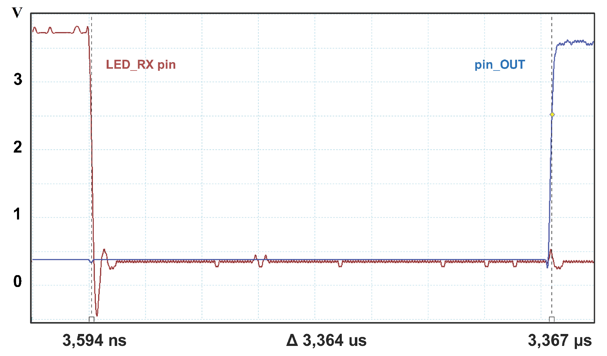
| 1 Gbps | 3.600 | 3.364 | 0.47 |
| Feature | [7] | [8] | [9] | [10] | [28] | This Work |
|---|---|---|---|---|---|---|
| Microprocessor | Yes | Yes | Yes | Yes | no | no |
| Encryption | AES (OFB) | AES (CBC) | AES (OFB) | DES | no | AES (GCM) |
| Authentication | HMAC (256) | HMAC (256) | HMAC (256) | MD5 | no | GMAC |
| Communication | Ethernet | Ethernet | Ethernet | local | Ethernet | Ethernet |
| Resources | ||||||
| Slice Registers | 13,600 | 10,124 | 9740 | - | 1083 | 4138 |
| Slice LUT | 13,305 | 13,470 | - | 7102 | 13,862 | 4748 |
| Block RAMs | 65 | 35 | 69 | - | 117 | 5.5 |
| DSP | 10 | 3 | 7 | - | - | - |
| Overhead (FPGA) | high | high | high | low | high | low |
© 2018 by the authors. Licensee MDPI, Basel, Switzerland. This article is an open access article distributed under the terms and conditions of the Creative Commons Attribution (CC BY) license (http://creativecommons.org/licenses/by/4.0/).
Share and Cite
Urbina, M.; Moreira, N.; Rodriguez, M.; Acosta, T.; Lázaro, J.; Astarloa, A. Secure Protocol and IP Core for Configuration of Networking Hardware IPs in the Smart Grid. Energies 2018, 11, 510. https://doi.org/10.3390/en11030510
Urbina M, Moreira N, Rodriguez M, Acosta T, Lázaro J, Astarloa A. Secure Protocol and IP Core for Configuration of Networking Hardware IPs in the Smart Grid. Energies. 2018; 11(3):510. https://doi.org/10.3390/en11030510
Chicago/Turabian StyleUrbina, Marcelo, Naiara Moreira, Mikel Rodriguez, Tatiana Acosta, Jesús Lázaro, and Armando Astarloa. 2018. "Secure Protocol and IP Core for Configuration of Networking Hardware IPs in the Smart Grid" Energies 11, no. 3: 510. https://doi.org/10.3390/en11030510
APA StyleUrbina, M., Moreira, N., Rodriguez, M., Acosta, T., Lázaro, J., & Astarloa, A. (2018). Secure Protocol and IP Core for Configuration of Networking Hardware IPs in the Smart Grid. Energies, 11(3), 510. https://doi.org/10.3390/en11030510