Article

A Wide Load Current and Voltage Range Switched Capacitor DC–DC Converter with Load Dependent Configurability for Dynamic Voltage Implementation in Miniature Sensors

College of Information and Communication Engineering, Sungkyunkwan University, Suwon 16419, Korea
*
Author to whom correspondence should be addressed.
Energies 2018, 11(11), 3092; https://doi.org/10.3390/en11113092
Submission received: 19 October 2018 / Revised: 3 November 2018 / Accepted: 6 November 2018 / Published: 8 November 2018

Abstract

:
Advancements in low power circuits and batteries have enabled the design of miniature sensors with tiny batteries. In such systems, implementing dynamic voltage scaling (DVS) is crucial for maximizing system lifetime. In this paper, a new switched capacitor (SC) converter that is capable of handling a wide range of load currents and output voltages is presented for on-chip DVS implementation. The proposed converter consists of multi-ratio multi-leaf SC stages and reconfigurable interconnect, enabling fine voltage resolution. The stage interconnect scheme enables cascaded or parallel connection of stages. The multi-leaf structure allows load-dependent switch size selection, offering a better trade-off between losses over a wide load range. A limited-voltage-swing switch-driving scheme allows efficient down-conversion from high battery voltage input. A prototype was fabricated in a 180 nm process, providing an output voltage with effective resolution of 16 mV over a load current range of 300 nA to 300 μA (1000×) from a 4 V battery. Efficiency greater than 62% and a peak efficiency of 77% are achieved under a light load (500 nA) over a voltage range of 400 mV to 1.6 V. Efficiency greater than 64% and a peak efficiency of 72% are achieved under a heavy load (200 μA) over a voltage range of 700 mV to 1.6 V.

1. Introduction

With the recent advancements in low power circuit design, packaging and battery technologies, the volumes of computing systems have been significantly reduced. With such a trend, numerous mm-scale miniature sensors have been demonstrated over the last decade [1,2,3]. These miniature sensors have been drawing attention since they can make traditional sensor systems more effective and energy-efficient. At the same time they also enable new volume-constrained applications such as implanted medical diagnostic sensors and monitoring sensors for an access-limited environment. However, the biggest concern for such miniature systems is the operation lifetime. Therefore, optimizing the use of energy stored in a battery is a key design goal for battery powered miniature sensor systems [1].
Miniature sensor systems are typically designed to spend most of their time in standby mode to minimize power consumption and maximize battery lifetime [1,2] but are periodically activated for short periods of time to perform their designated functions. During standby mode, the current consumption of such systems is on the order of sub-microamperes. On the other hand, the active mode current consumption ranges from a few microamperes to hundreds of microamperes depending on the task being performed [3]. Therefore, the power management unit in miniature sensor systems should be able to efficiently handle a load current ranging from sub-microamperes to hundreds of microamperes.
To minimize standby power, the supply voltage needs to be reduced to the minimum voltage level at which data can be retained in standby mode. Conversely, in active mode, the supply voltage should be increased for better performance and stable operation [4,5]. This implies that the power management unit in miniature sensor systems should also be capable of handling a wide voltage range.
Providing a wide range of voltage conversion ratios for DC–DC conversion is also an important feature for the power management unit in miniature sensors. To enable dynamic voltage scaling (DVS) for energy efficient operation, a range of output voltages should be generated from the fixed battery voltage. Moreover, since the battery voltage can also vary over time, various conversion ratios are also required to provide constant regulated voltage.
Switched capacitor (SC) DC–DC converters are good candidates for power management units in miniature systems. By utilizing integrated capacitors as passive elements, they can provide fully integrated solutions that are capable of handling microwatts of power. This enables a cost-effective small form factor, which typically cannot be offered with inductor-based buck converters, where one of the following is required: a bulky off-chip inductor [6,7,8]; an expensive on-chip inductor [9,10]; or a complicated post-fabrication process [11]. The large conversion ratio requirement also prohibits the use of low dropout regulators (LDOs) in such systems since the efficiency of an LDO is proportional to its conversion ratio [12,13,14].
However, some challenges must be overcome for SC converters to fulfill the aforementioned requirements. SC converters can provide only rational conversion ratios, which can be represented as
V O U T = n m · V I N
where ‘n’ and ‘m’ are integers determined by the converter topology. This implies that SC converters can only provide limited resolution on regulated voltage, which complicates the implementation of DVS for efficient operation. Moreover, maintaining efficient operation in both active and standby modes is also non-trivial: it requires efficient clock generation over a wide frequency range and driving switches with limited voltage swing may be required since the switching loss with full battery voltage swing can be significant in standby modes.
A number of SC DC–DC converter topologies applicable to miniature systems have been reported in recent years [15,16,17,18,19,20,21,22]. Many single-stage SC structures [15,16,17,18,19] have been introduced that provide very high efficiency but only at a few ratios, which limits their application to a narrow voltage range. A few multi-stage SC converters, such as successive approximation (SAR) [20], recursive-tertiary [21], and recursive-binary [22] DC–DC converters, have been reported that provide high efficiency over a wide output voltage range. However, these converters are only optimized for active operation state, and the minimum load current is on the order of a few microamperes. Therefore, the efficiency of these architectures in standby mode is low. For example, the efficiency of SAR [20] at near threshold voltage (0.4–0.7 V) degrades drastically to less than 40% when the load current reaches 1 μA or less. A reconfigurable SC structure presented in [21] achieves a higher number of conversion ratios with fewer SC stages, but with full input voltage (2.5 V) swing switch driving. Such full-swing switch-driving is acceptable with heavy load condition, since conduction loss is the dominant loss. However, with a light load condition in standby mode, which could be the dominant operating mode in heavy duty-cycled wireless sensor nodes (WSN) and IoT systems, switching loss become the dominant loss contributor and driving switches with voltages significantly higher than their threshold voltage can be a waste of power, resulting in inefficient operation in standby mode. Since the WSNs often utilize high energy density batteries with high output voltage (~4 V), unnecessary loss with full-swing switch-driving can be significant.
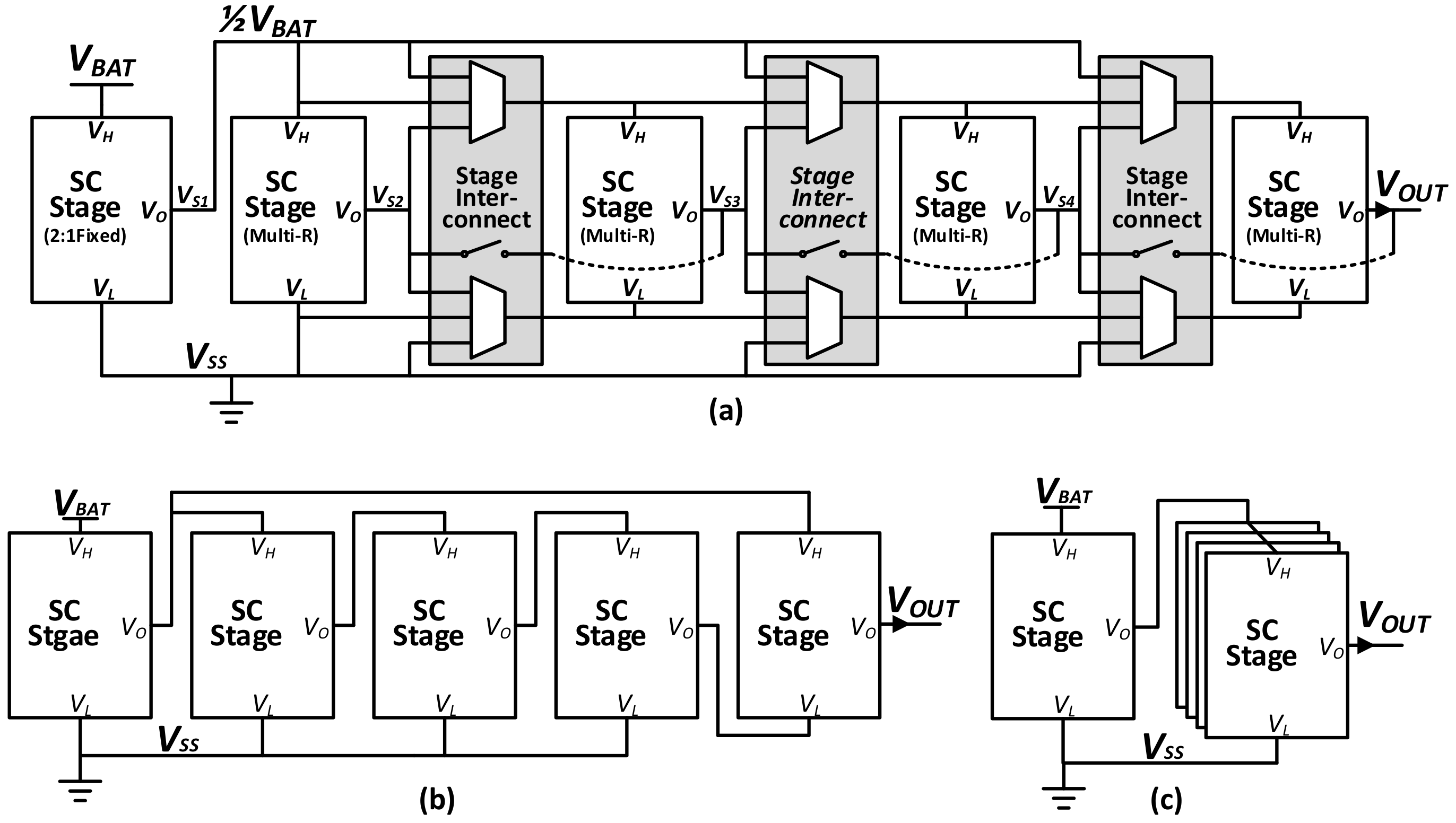
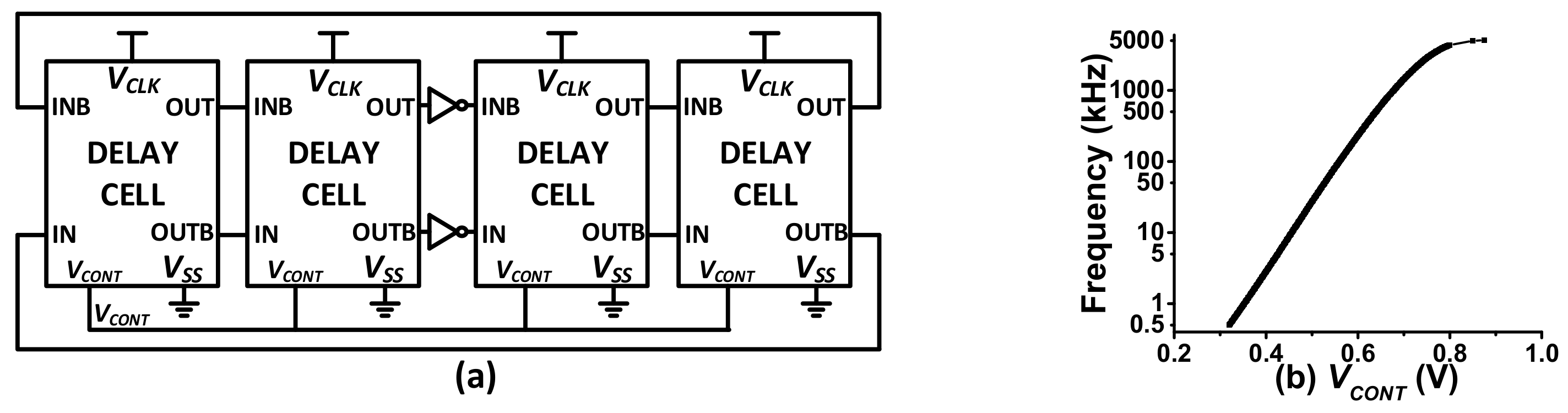
In this paper, a multi-stage and multi-leaf reconfigurable SC converter with load-dependent reconfigurability and limited-swing switch-driving scheme [23] is presented. The proposed converter consists of multi-ratio multi-leaf SC stages and reconfigurable interconnect, enabling fine voltage resolution with switch width modulation, which is required for DVS over a broad load current range. The reconfigurable stage interconnect (RSI) scheme allows cascaded or parallel connection of stages depending on the output voltage and current demand. The multi-leaf structure allows load-dependent switch size selection, offering a better trade-off between conduction loss and switching loss over a broad current range. A symmetric leakage-based clock generator allows efficient clock generation over a wide frequency range with balanced duty cycle. As switching loss is proportional to the square of the driving voltage, the full input voltage swing driving scheme degrades efficiency at the voltage conversion from high battery voltage. The proposed SC converter switches are driven by a limited voltage swing driving scheme, which makes switching loss independent of input voltage, enabling efficient voltage conversion with high battery voltage.
Various types of batteries can be used for powering miniature systems. Depending upon the battery type, the output voltage may vary from 1.2 to 4.0 V [15,16,17,18,19,20,21,22]. This work uses a Li-ion battery where the voltage can vary from 3.6 to 4.2 V. This is typically the maximum voltage level used for stand-alone miniature systems and thus represents the worst case scenario. The same structure applied at a lower input voltage (e.g., 2.0 V) can result in improved efficiency.
For power electronics applications with at least a few milli-watts of power, electromagnetic interference (EMI) analysis, like that presented in [24,25,26] is essential to determine compliance to the EMI regulations for satisfactory operation of nearby circuits. However, the proposed SC converter is implemented for low power applications, where maximum power demand is less than 1 mW, and fully integrated implementation makes EMI negligible. Therefore, EMI analysis of the proposed SC converter has not been considered in this work.
The remainder of this paper is organized as follows: Section 2 provides a detailed analysis of the loss mechanisms in the SC converter at varying operating conditions. Then the detailed architecture of the proposed converter is presented in Section 3. In Section 4, the measurement results are shown to verify the effectiveness of the proposed approach, and Section 5 concludes the paper.

2. Loss Analysis and Power Delivery Capability of an SC Converter

In SC converters, there are two fundamental loss mechanisms, namely conduction loss and switching loss. As the output load current and voltage change, both of these losses can vary drastically; hence, careful balancing between these losses is required for optimized power delivery. Therefore, analyzing the trade-off between these losses is the first step in implementing an efficient SC converter suitable for operation over wide voltage and current ranges.
SC converters rely on energy and charge transfer between flying capacitors, which act as voltage sources. Since the voltage conversion is achieved by connecting flying capacitors in series or parallel, the voltage generated by an SC stage is determined by its topology and the summation or subtraction of flying capacitor voltages. Therefore, unlike the inductor-based converters where conversion ratios can be continuously adjusted by controlling the switching frequency or duty cycle, only discrete conversion ratios can be generated with SC converters.
The number of available conversion ratios in an SC stage is determined by the number of flying capacitors and charge transfer phases per operation cycle. For a given number of flying capacitors, more voltage conversion ratios can be implemented by increasing the number of charge transfer phases [21]. However, this limits the net conduction time of each transistor, resulting in reduced efficiency. For example, each phase lasts up to 50% in a 2-phase operation and up to 33% in a 3-phase operation. Therefore, assuming the same operation frequency, a 3-phase operation requires a larger switch to conduct the same amount of charge in a shorter conduction time, resulting in greater switching loss.
This work focuses on the efficient operation of an SC converter over varying load currents and voltages, including light load cases where the control and drivers are the dominant loss. A 2-phase clock is used owing to the simple drivers and control schemes.
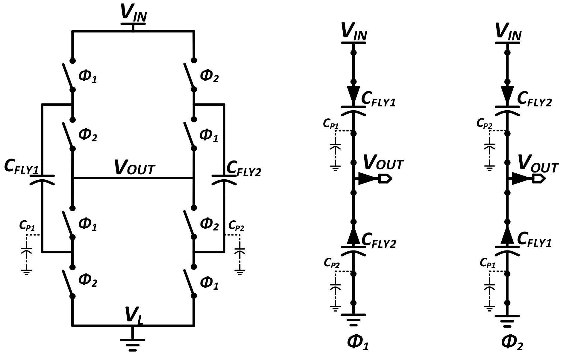
To illustrate the basic tradeoff between switching and conduction loss, a simple 2:1 step-down SC converter, shown in Figure 1, was analyzed at light and heavy load conditions. Table 1 provides a list of the parameters used in analysis and their measurement units. The converter presented in Figure 1 operates with a 2-phase non-overlapping clock. During phase ϕ1, the top and bottom terminals of CFLY1 are connected to the battery (VIN) and output (VOUT), respectively; thus, drawing charge from the battery as charges are taken at the output node. On the other hand, CFLY2 is connected between VOUT and ground (VSS), supplying charge to the output node. During phase ϕ2, the flying capacitors switch their positions such that CFLY2 is charged, and CFLY1 is discharged. Periodic charging and discharging of the flying capacitors results in ripple voltage (ΔV) at the flying capacitors, which can be written as
Δ V = I L O A D 2 C F L Y f S W
where ILOAD is the load current, and fSW is the switching frequency. Such ripple incurs power loss, which can be categorized as conduction loss. This is an inevitable loss in SC converters because power is delivered through charge transfer via transistors, and a voltage difference between source and drain is required for charge transfer to be enabled. The conduction loss due to ripple voltage, as investigated in detail in [27,28], can be given as
P C o n d . Δ V = I L O A D . Δ V 2 =   I 2 L O A D K C C F L Y f S W
where KC is the loss coefficient related to the converter topology. Ideally, switches in SC converters are assumed to have zero resistance, but real switches have finite resistance, which leads to additional conductance loss. Conduction loss due to switch resistance is given in [27] as
P C o n d . S w = I 2 L O A D R O N K S W W S W
where RON is the switch resistance per unit width during the “on” state, WSW is the total width of the switches, and KSW is the topology-dependent loss coefficient. Therefore, the total conduction loss can be calculated by adding the loss due to voltage ripple and the switch conduction loss as follows:
P C o n d = P C o n d . Δ V +   P C o n d . S w P C o n d = I 2 L O A D K C C F L Y f S W +   I 2 L O A D R O N f S W W S W
The other type of loss in SC converters is switching loss. One of the major contributors to switching loss is the parasitic capacitance associated with flying capacitors. For on-chip capacitors, both the top and bottom plates have associated parasitic capacitances. For simplicity, the switching loss associated with the top and bottom plate parasitic capacitances is referred to as bottom plate switching loss (PSw.Bot) since the bottom plate parasitic capacitance is much larger than the top plate parasitic capacitance in most integrated capacitors. For the converter in Figure 1, the parasitic capacitor CP1 associated with CFLY1 is charged to the output voltage (VOUT) during ϕ1. During the following phase, ϕ2, CP1 is discharged to ground, resulting in bottom plate switching loss defined as
P S w . B o t = K P V 2 O U T C P f S W
where KP is the topology-dependent loss coefficient.
Another type of switching loss is the power consumed for the driving gate capacitances of all of the switches. This loss can be written as
P S w . G a t e = V 2 S W C G a t e f S W
where VSW is the voltage swing at the gate, and CGate is the total gate capacitance. Adding Equations (6) and (7) yields the total switching loss (PSW):
P S w = [ K P V 2 O U T C P f S W ] + [ V 2 S w C G a t e f S W ]
Therefore, adding Equations (5) and (8) provides the total loss in an SC converter (PLOSS) as follows:
P L O S S = [ ( I 2 L O A D K C C F L Y f S W ) + ( I 2 L O A D R O N K S W W S W ) ] + [ ( K P V 2 O U T C P f S W ) + ( V 2 S W C G a t e f S W ) ]
The above equation provides insight on the tradeoff between conduction loss and switching loss in an SC converter. For conduction loss, fSW and WSW are in the denominator, whereas for switching loss, fSW and CGate are in the numerator. Both WSW and CGate are proportional to the switch size. This implies that increasing the operation frequency and transistor width will reduce conduction loss and increase switching loss, whereas decreasing the frequency and transistor width will have the opposite effect.
Meanwhile, the power delivery capability (PLOAD) of an SC converter can be defined as [16]
P L O A D = K L C F L Y V O U T V d r o p f S W
where KL is the loss coefficient that is dependent upon the SC converter topology, and Vdrop is the deviation from the ideal no-load voltage (VNL). Equation (10) indicates that a light load can be provided with a small Vdrop at a low fSW, resulting in an optimal operating voltage (VOPT) near VNL. In contrast, heavy load operation results in a large Vdrop at a high fSW, resulting in a VOPT much lower than VNL.
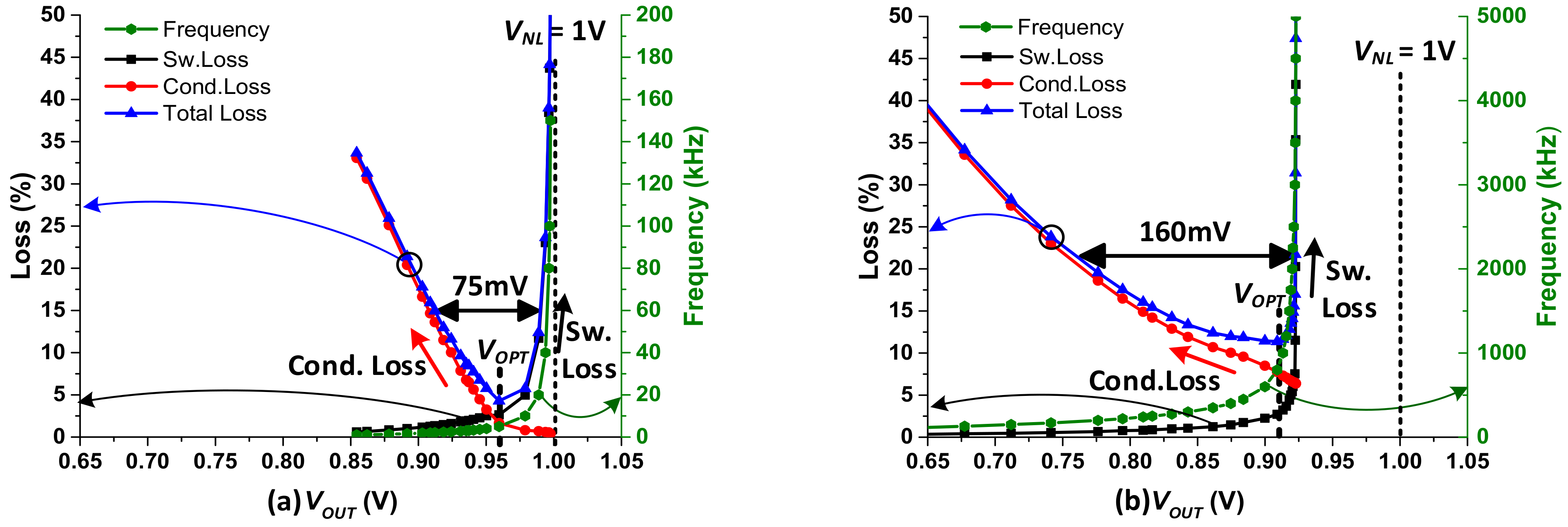
Figure 2 presents the simulation results for a 2:1 down-conversion with 2 V input (VNL = 1 V) in a single stage of the SC converter shown in Figure 1. The required operation frequency and power losses expressed as percentages are plotted as functions of the output voltage. For simulation, the parasitic capacitances CP are kept at 3% of the flying capacitance, which is a typical value for high metal layer metal–insulator–metal (MIM) capacitors.
With a light load of 500 nA, the total loss is minimized at an output voltage of approximately 0.96 V (VOPT), as shown in Figure 2a. To increase the output VOUT above VOPT, the frequency must be increased exponentially, which results in an exponential increase in switching loss. On other hand, to reduce VOUT below VOPT, the frequency must be decreased, lowering the corresponding switching loss. However, under light load conditions, the optimal operation is achieved at low frequency (~8 kHz in the presented case), where the output voltage ripple is sensitive to change in frequency. As the frequency is reduced, the voltage ripple increases drastically, resulting in a sharp increase in conduction loss, as can be found in Equation (2). These factors result in a narrow convex-shaped total loss curve whose VOPT is close to VNL for an SC converter under light load scenarios.
When a heavy load of 100 μA is applied to the identical SC converter, the switching and conduction losses change as shown in Figure 2b. The total loss is minimized at lower VOPT, which is around 0.91 V with fSW ≈ 830 kHz. To generate VOUT higher than VOPT, the frequency must be increased exponentially. This results in an exponential increase in switching loss, rendering the region between VOPT and VNL inefficient. However, under heavy load, the SC converter operates with a higher frequency (830 kHz vs. 8 kHz in this example), and the output ripple is less sensitive to change in frequency compared with the low load case. Therefore, as VOUT is decreased with lower frequency, the voltage ripple and consequent conduction loss increase at a slower rate. The outcome is a wider convex-shaped loss curve, resulting in wider efficient region around VOPT compared with the low load scenario.
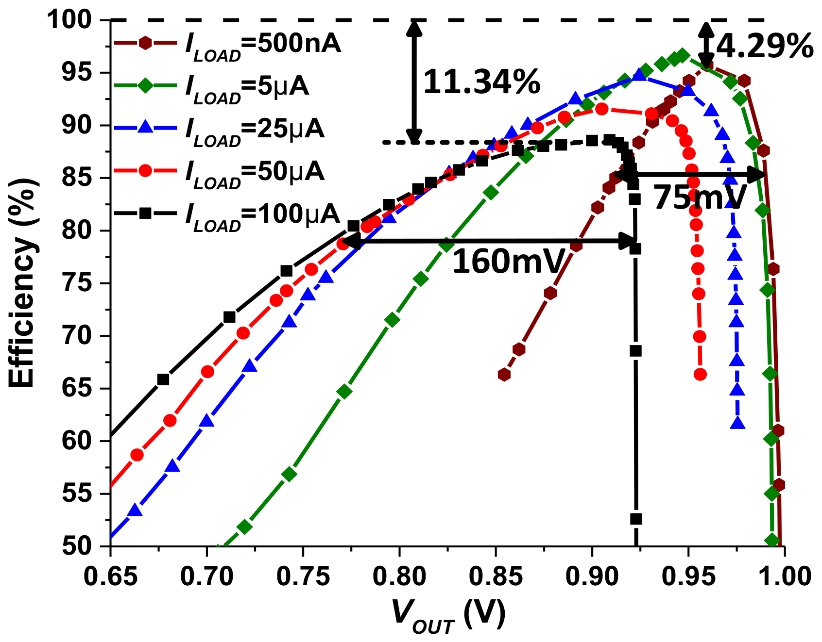
The loss curves in Figure 2 can be translated into efficiency curves, as shown in Figure 3 with additional simulation results for intermediate load conditions. The following conclusions can be drawn from these simulation results.
(1) The efficiency curves are narrower under light load conditions than under heavy load conditions. For example, the voltage range that keeps the efficiency within 10% of the peak efficiency is 75 mV for the 500 nA light load and 160 mV for the 100 µA heavy load. This implies that to maintain efficient operation over a given voltage range, more efficiency curves providing different VNL are required for light load conditions. Since VNL is determined by the conversion ratio, to maintain efficient operation for a given VOUT range, more conversion ratios should be provided for light load conditions, and relatively fewer conversion ratios are required for heavy load conditions.
(2) The power loss at the optimum operation voltage (VOPT) at a single stage of the SC converter is significantly higher (11.3%) with a heavy load (100 µA) and lower (4.3%) with a light load (500 nA). This implies that while cascading SC converter stages can provide finer voltage resolution, they result in significant loss under heavy load. Therefore, for heavy load conditions, the number of cascaded stages should be minimized.
Considering the efficiency trends stated above, the following operation strategies can be developed for an SC converter targeted for wide load current and voltage ranges:
(1) For light load conditions, each conversion ratio is efficient only over a very small voltage range. Therefore, providing many conversion ratios and fine resolution by cascading SC converter stages is preferred since stage loss is small.
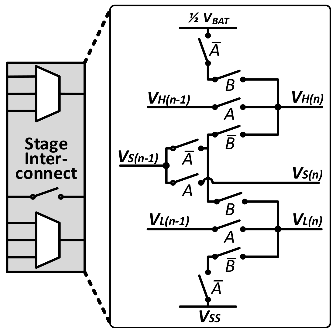
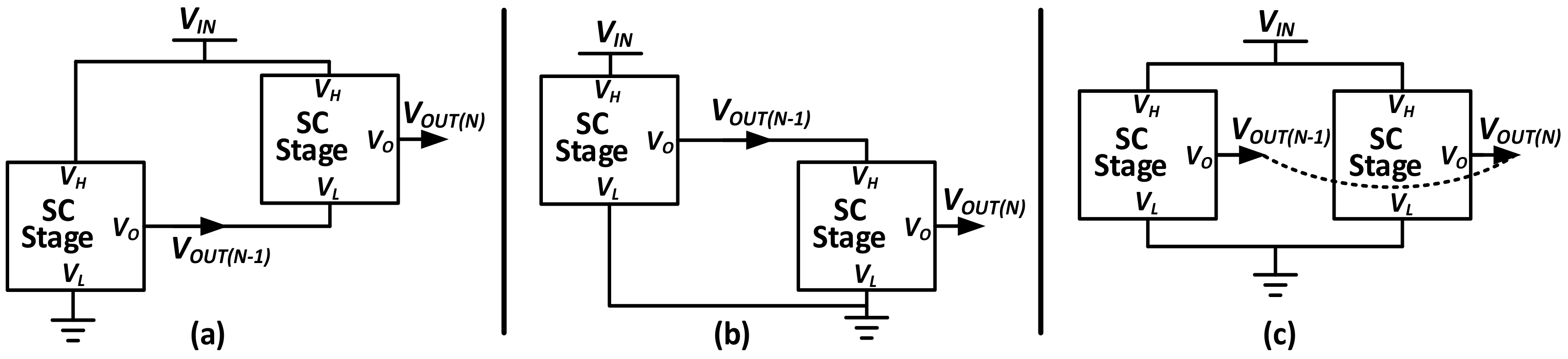
(2) For heavy load conditions, each conversion ratio is efficient over a relatively wider voltage range. Therefore, fewer conversion ratios are required, and the number of cascaded stages can be reduced. Since the stage loss is larger, the number of cascaded stages should be minimized. In this case, the stages that are cascaded for providing fine voltage resolution under light load conditions can now operate in parallel configuration. This approach increases the effective flying capacitor and switch size and reduces conduction loss, which is the dominant loss factor under heavy load conditions.
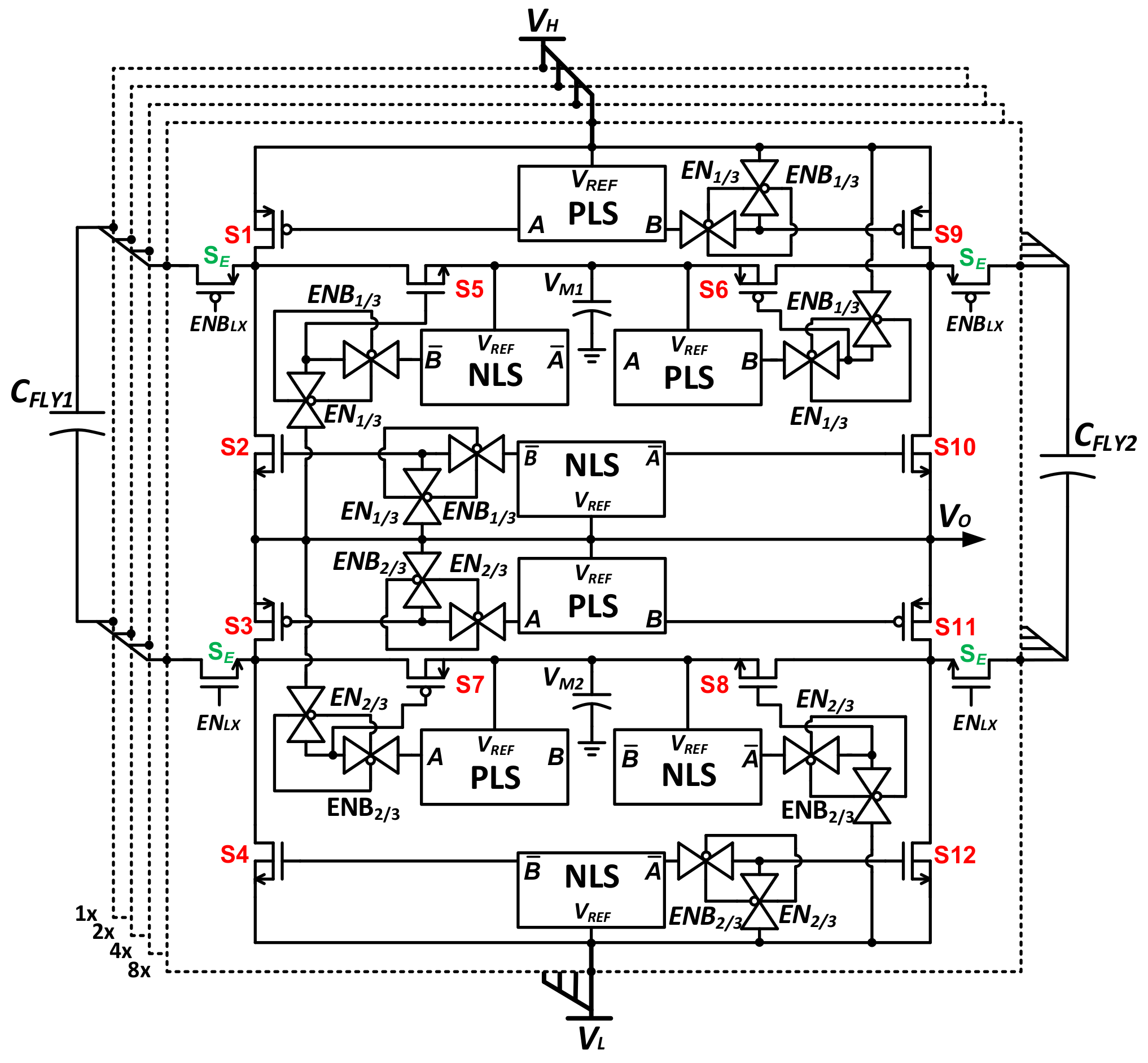
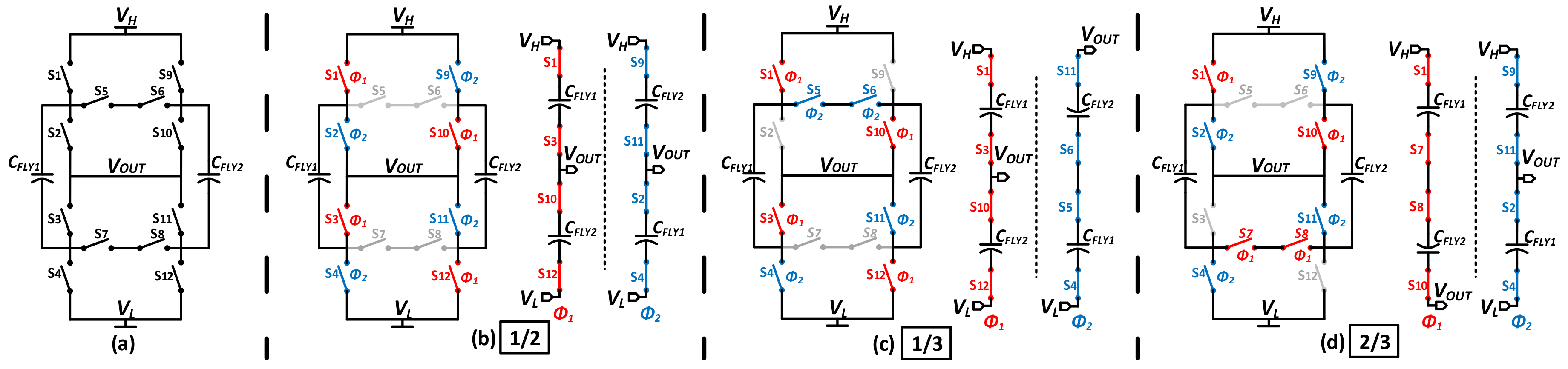
(3) To minimize the number of cascaded stages, an SC stage structure that can provide multiple conversion ratios is preferred over an SC stage with a fixed 2:1 ratio. The maximum number of achievable conversion ratios using a 2-phase clock and two flying capacitors is three [29]. Therefore, an SC stage topology with three variable ratios is adopted, which can efficiently provide fine resolution with fewer SC stages by limiting conduction loss.
(4) To further optimize loss, especially with the light load conditions, it is desirable to adjust the switch size, i.e., the transistor width, of an SC converter, as shown in Equation (9). By adjusting WSW and CGate, efficiency can be improved by balancing conduction and switching losses.
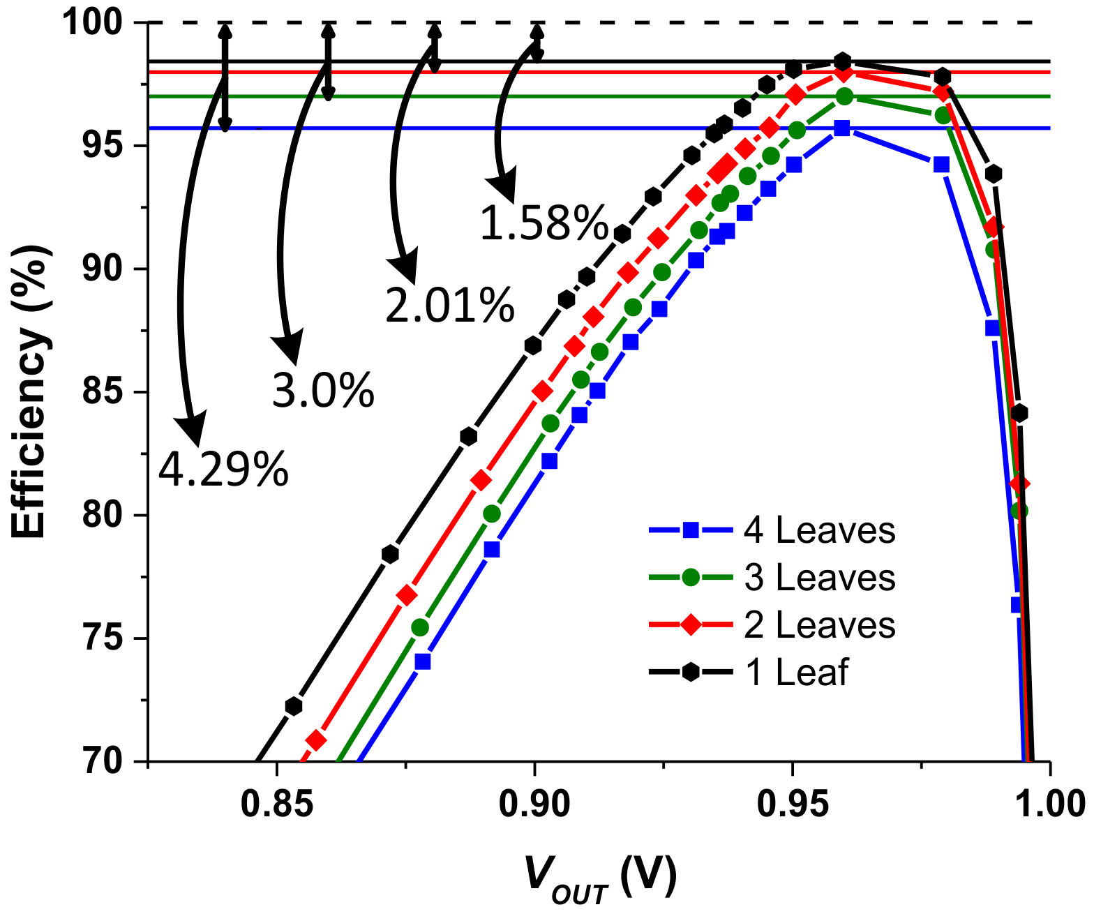
In Figure 3, where an identical switch size is used for various load currents, the peak efficiency at ILOAD = 5 µA appears to be higher than at ILOAD = 500 nA. This is because the switch size is too large for the 500 nA load, incurring unnecessary switching loss. Therefore, in addition to lowering the frequency for light load conditions, the switch size must also be reduced. Figure 4 shows the simulation results for the 2:1 converter with binary-sized switches with ILOAD = 500 nA. With the reduced switch size, peak efficiency improvement is observed under a light load by eliminating the excessive capacitance load of the power switch in Equation (7).
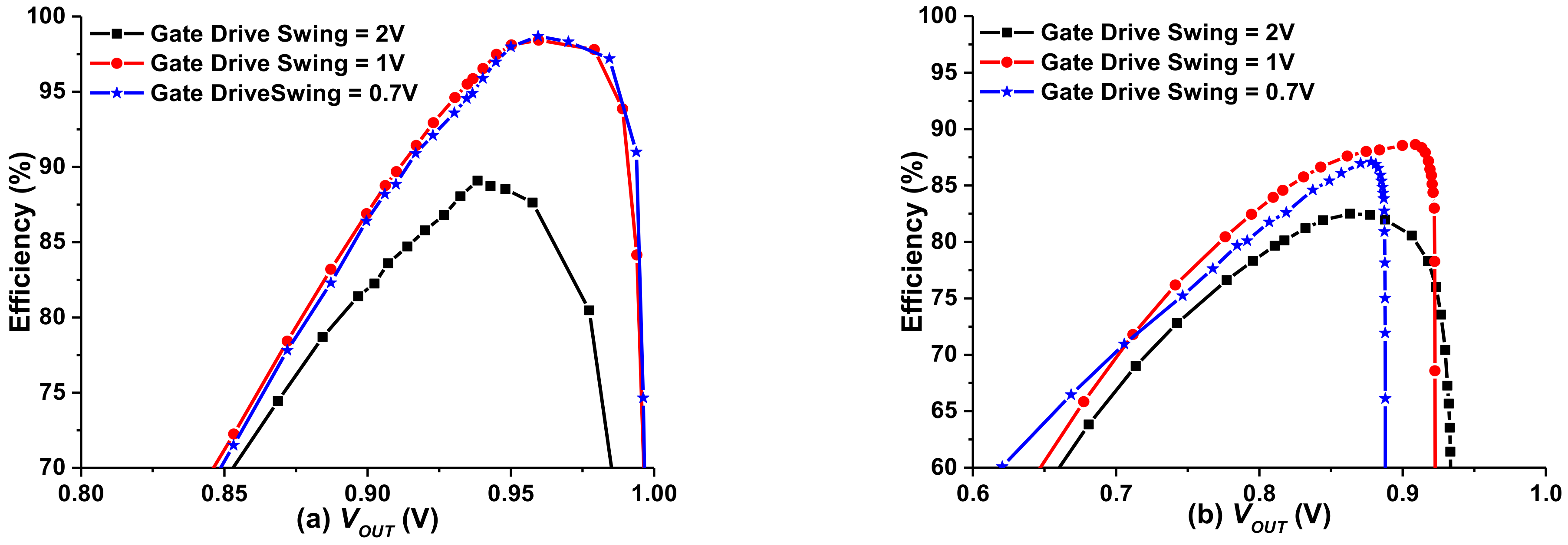
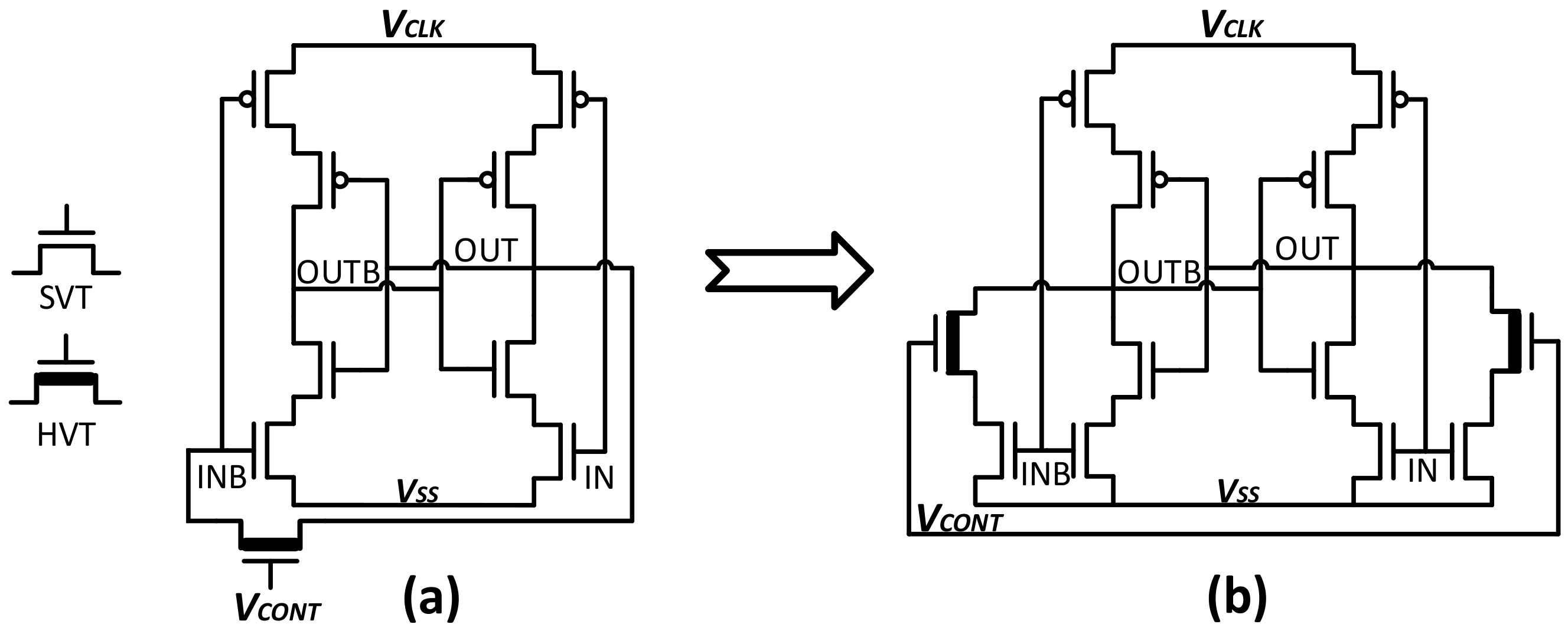
Since the switching loss for switch driving is proportional to the square of VSW as shown in Equation (7), a switch driving scheme independent of input battery voltage VIN is desirable and the optimal gate driving voltage depends upon the threshold voltage of switch. Figure 5 shows how efficiency changes with varying switch driving voltage swing for a 2:1 converter at ILOAD of 500 nA and 100 µA respectively. With both low and high load conditions, driving switches with unnecessarily high VSW of 2 V significantly drops the efficiency due to a large switching loss. However, with a high 100 µA load, utilizing too low VSW could also be a problem since the insufficient overdriving voltage can make RON high, increasing conduction loss. Therefore, proper VSW, which is technology dependent, should be carefully chosen to optimize both low and high load conditions.

3. Proposed SC Converter Architecture

Based on the four strategies discussed in the previous section, a reconfigurable SC converter suitable for wide load current and voltage ranges was proposed. The top level architecture of the proposed SC converter is presented in Figure 6a. To provide many voltage conversion ratios, five SC stages are utilized. The first SC stage has a fixed ratio of 2:1, whereas the following four SC stages are configurable to three different ratios, namely 1/3, 2/3, and 1/2. The multi-ratio SC stages are connected through reconfigurable stage interconnects (RSIs), which provide the flexibility of cascaded or parallel connections among stages, depending upon the load condition. With a light load, the SC stages can be connected in series, as shown in Figure 6b, whereas for a heavy load, the later four stages can be connected in parallel, as shown in Figure 6c. Mixed series–parallel connections can be also employed for intermediate loads.

3.1. Multi-Ratio and Multi-Leaf SC Stage Structure

Figure 7 illustrates the structure of multi-ratio and multi-leaf SC stages. Each SC stage consists of four switching leaves with binary-sized switches. Under light load conditions such as sub-µA, the switching loss is the major loss contributor; hence, only the minimum-sized leaf is activated to minimize the switching loss. As the load increases, leaves with larger switches can be activated to reduce conduction loss at the cost of additional switching loss. When only a subset of available leaves are activated, it is still better to operate with the maximum available flying capacitance to minimize conduction loss, as demonstrated in Equation (3). Therefore, flying capacitors are directly connected to the minimum leaf that is always active. Larger leaves are enabled/disabled by connecting switches to flying capacitors by controlling enable switches SE with control signals (ENLX, ENBLX).
Each switching leaf consists of 12 power transistors (S1–S12) and the associated drivers with activation control to provide three discrete conversion ratios. To minimize switching overhead, instead of VIN, limited clock swing is used for driving all switches. The P-channel MOSFET (PMOS) are driven by P-type level shifters (PLS), whereas the N-channel MOSFET (NMOS) are driven by N-type level shifters (NLS), as will be described in detail in subsection 3.4. A simplified diagram of a multi-ratio SC stage leaf is shown in Figure 8a. With the given structure, conversion ratios of 1/2, 1/3, and 2/3 can be achieved, as shown in Figure 8b–d, respectively, by driving eight power transistors with 2-phase-interleaved signals (red or blue switches in Figure 8) and disabling the rest of the four transistors (grey switches in Figure 8). Table 2 summarizes the enabled switches and phase sequence for each mode of operation. The enabled switches are closed in one phase and open during the alternate phase, e.g., switch S1 is closed during ϕ1 and open during ϕ2. Switches labeled as disabled are always open during the corresponding mode of operation, e.g., switch S2 is always open in 1/3 mode, but in 1/2 and 2/3 modes, it is closed during ϕ2 and open during ϕ1.
The power switches in the SC stage’s leaf can be categorized into the following two types depending on the availability of the stable source voltage:
  • Boundary switches (S1–S4, S9–S12)
  • Middle switches (S5, S8)
Boundary power switches have a stable voltage (VH, VL or VOUT) at the transistor’s source terminals. This stable source voltage is used as reference for generating limited voltage swing on/off control signal by the level shifters, which are described in more detail later. However, Middle switches lack such a topology-inherent stable voltage at the source terminals, which is required for level shifter drivers. To address this challenge, local capacitors CM1 and CM2 are placed to implement local reference voltages VM1 and VM2, as shown in Figure 7. These voltages converge to deterministic voltages depending on the operating conversion ratio. Thus middle switches can be driven with limited voltage swing by using local reference for level shifter drivers.
Boundary switches can be disabled by shorting the gate with the source terminal through stage disable switches (ENX, ENBX in Figure 7). However, to disable Middle switches, local reference voltages (VM1 and VM2) cannot be used since they are not deterministic when adjacent transistors are disabled (i.e., always off). Therefore, Middle switches are disabled by connecting the gate to the suitable stable power/ground rail, which is at a potential sufficient to keep the switches turned off. For example, when disabled, the gate terminal of S5 is connected to VOUT, whereas the gate of S6 is connected to VH.
Optimal capacitance allocation for flying capacitors amongst SC converter stages depends upon the conversion ratio configuration and interconnection scheme of the stages. Each configuration requires a unique optimal distribution of flying capacitors, which cannot be easily adjusted with a multi-stage structure. Thus the binary distribution of [21] with the smallest flying capacitor at the first and the largest at the last stage is opted for.

3.2. Reconfigurable Stage Interconnect

Figure 9 illustrates the implementation of the reconfigurable stage interconnection (RSI) scheme. RSI provides a differential input voltage (VHVL) to each SC stage, which can be configured with 2-bit control signals An and Bn. Through RSI, the next stage’s high input VH(n) can be connected to the previous stage’s high VH(n−1) or intermediate power supply (first stage output ½VBAT) or the previous stage’s output VS(n−1). Likewise, the next stage’s low input VL(n) can be connected to the previous stage’s low input VL(n−1) or ground node VSS or the previous stage’s output VS(n−1). By selecting the appropriate connection, RSI schemes operate in one of the modes illustrated in Figure 10, and the corresponding control bits are summarized in Table 3. In the first two modes shown in Figure 10, two adjacent stages are series connected to generate an output voltage whose value is between the earlier stage’s output voltage [VOUT(N−1)] and power/ground. On the other hand, in the last mode, two stages are parallel connected to increase the effective switch width and flying capacitance. Such a reconfigurable structure allows voltage generation with fine resolution for light loads and reduction of conduction loss for heavy loads as needed.
It must be noted that the output of the first stage (VS1 = ½VBAT) is kept as the power rail for the remainder of the stages since the target output voltage is <2 V. It is also worth noting that providing connection to power/ground recursively at each stage helps to reduce cascading loss due to direct charge transfer from power/ground rails [21]. Thick oxide devices are used for the first SC stage since it has to tolerate high VBAT. However, the maximum voltage that the rest of the stages should handle is limited to 2 V, which allows for the use of thin oxide devices, significantly improving efficiency.

3.3. Load-Dependent Configurability

The use of a multi-ratio SC stage along with RSI results in (3 × 2 = 6) conversion ratios per stage, excluding the parallel connection case. Therefore, in the presented topology, setting the first stage as a fixed 2:1 converter and the rest of the four stages as multi-ratio with three RSIs in between, results in 1 × 63 × 3 = 648 possible configurations. Because many configurations provide duplicated conversion ratios, there are 125 discrete conversion ratios over the voltage range of 0–2 V, which translates into an average voltage resolution of 16 mV when the input battery voltage is 4 V. Such fine voltage resolution is vital for efficient operation under light load conditions where each configuration is efficient for only a very limited voltage range.
Figure 11 illustrates example operations of a reconfigurable SC converter. In Figure 11a, stage 1 provides a fixed VS1 = 1/2 conversion. Stage 2 is configured in 2/3 ratio with high input connected to stage 1 output (VH2 = VS1) and low input to ground (VL2 = VSS), which results in VS2 = 1/3. Then in the third stage, VH3 is connected to the previous stage output VS2, and VL3 is connected to VSS by applying a configuration code of ‘00’ at the first RSI. The third stage converter is configured to 2/3 ratio, resulting in VS3 = 2/9. At the fourth stage, assigning VH4 = VS3 and VL4 = VSS by applying a configuration code of ‘00’ at the second RSI and using 1/3 ratio provides VS4 = 2/27. At the fifth stage, assigning VH5 = VS1 and VL5 = VS4 by applying an RSI configuration code of ‘01’ and using 1/2 ratio results in VOUT = [VS4 + (VS1VS4)/2] = 31/108. The overall conversion ratio of 31/108 provides a no load voltage of VNL = 1.148 V when VBAT = 4.0 V. Figure 11b presents the case of a conversion ratio of 7/24, which results in VNL = 1.167 V. Since four stages are sufficient to generate this ratio, parallel connection can be applied to the third and fourth stages to reduce conduction loss.
A multi-ratio multi-leaf SC converter with RSI provides load-dependent configurability for optimal voltage conversion operation. Depending on the system load condition, the conversion ratio and number of activated leaves in the proposed SC converter can be changed to provide an output voltage near VOPT under new operating conditions. An example case is illustrated in Figure 12 where the target output voltage is VOUT = 0.725 V from VBAT = 4.0 V. Under 500 nA loading, only minimum-sized leaves are enabled, and the conversion ratio of 5/24 is used, which provides VNL = 0.833 V. This requires a cascade length of four stages, as shown in Figure 12a, and 68.1% conversion efficiency could be obtained at target VOUT. When the load is increased to 10 µA, a higher conversion ratio is required to provide the same VOUT because the optimal operating point in a given conversion configuration moves away from VNL as the load is increased (Equation (10)). Therefore, the conversion ratio should be increased to 2/9 in Figure 12b (VNL = 0.889 V) with two leaves enabled, resulting in 66.3% efficiency. When the load is further increased to 200 µA, maximizing parallel connection and activation of all leaves are required. Therefore, the conversion ratio changes to 1/4 (VN L= 1.0 V) with a cascade length of two stages, as shown in Figure 12c, achieving 64% efficiency. It is worth mentioning that if the configuration optimized for 500 nA is used for 200 µA, efficiency drops to <27%, highlighting the effectiveness of reconfigurable SC topology.

3.4. Switch Driver and Clock Voltage

As discussed in Section 2, the switching loss for the driving gate has quadratic dependence on the voltage swing, as shown in Equation (7). Therefore, to minimize switching loss, rather than using full input voltage swing (VBAT), reduced clock swing is desired for driving switches. However, such reduced clock swing cannot be directly applied for driving MOSFETs, which are at a different potential, hence a cross-coupled level shifter scheme [20] is utilized. For driving PMOS, a P-type level shifter (PLS in Figure 7) is implemented, and for driving NMOS, an N-type level shifter (NLS in Figure 7) is implemented, as shown in Figure 13.
For an N-type level shifter, when the clock is low, the gate driving voltage should be set to the source voltage to turn off the target NMOS. When the clock is set high, the potential at the gate terminal should be increased by a preset voltage swing with regard to the source voltage, thus turning on the target NMOS. Similarly, P-type level shifters drive PMOS by lowering the gate potential with regard to the source voltage when the clock phase is low. This operation is achieved by capacitive coupling. For triggering level shifters, 2-phase non-overlapping clocks (ϕ1, ϕ2) are utilized to eliminate the possibility of turning on transistors on opposite phase together. Clock swings applied to target NMOS/PMOS are identical to the swing of ϕ1 and ϕ2. To reduce switching loss, the output voltage of the second stage is used for generating ϕ1 and ϕ2. For the first stage where a thick oxide device is utilized, higher voltage (½VBAT) is used for generating ϕ1 and ϕ2.

3.5. Leakage-Controlled Clock Generator

For efficient operation over a wide load current range, a wide clock frequency range from a few kHz to MHz is required. In addition, a balanced duty cycle is required for optimal utilization of the capacitor. This is because an unequal duty cycle results in unequal charge distribution among flying capacitors, which eventually results in larger ripple at stage outputs and corresponding higher conduction loss.
In this work, a leakage-controlled delay cell-based clock generator is presented for achieving a wide frequency range with an even duty cycle. A leakage-controlled delay cell structure was proposed earlier in [30,31] for energy-efficient clock generation over a wide frequency range. This clock generator controls its output frequency by controlling the amount of leakage current injected to accelerate oscillation by adjusting the control voltage (VCONT). However, as shown in Figure 14a, leakage control was only provided between IN and OUTB branch, whereas no control was applied to the other branch (INBOUT). This asymmetry in delay cell structure results in uneven duty cycle.
To address this issue, a symmetric leakage-controlled delay cell structure was proposed as shown in Figure 14b. The modified structure consists of two symmetric leakage control paths, one for each flipping branch. By series connecting these delay cells as shown in Figure 15, an energy-efficient clock generator with even duty and a wide frequency range could be designed. The proposed structure generates a clock with approximately 50% duty over the frequency range from 100 s of Hz to a few MHz. Note that high threshold voltage devices are used in the leakage control path to provide fine control over the leakage current, resulting in fine frequency steps.
In the proposed SC converter, leakage control voltage (VCONT), which is used for clock generator frequency control, can be also used for controlling the number of activated leaves in the SC converter stages. As load current increases, VCONT and the corresponding frequency should be increased, as shown in Figure 15b. Therefore, VCONT indirectly represents the amount of load current the SC converter is currently handling. By comparing VCONT with preset reference voltages, the appropriate number of leaves can be activated. Figure 16 shows the reference comparison circuitry for leaf control. Reference voltages are generated from a diode stack and made tunable to account for variations. As VCONT increases, additional leaves are gradually added.

4. Measurement Results

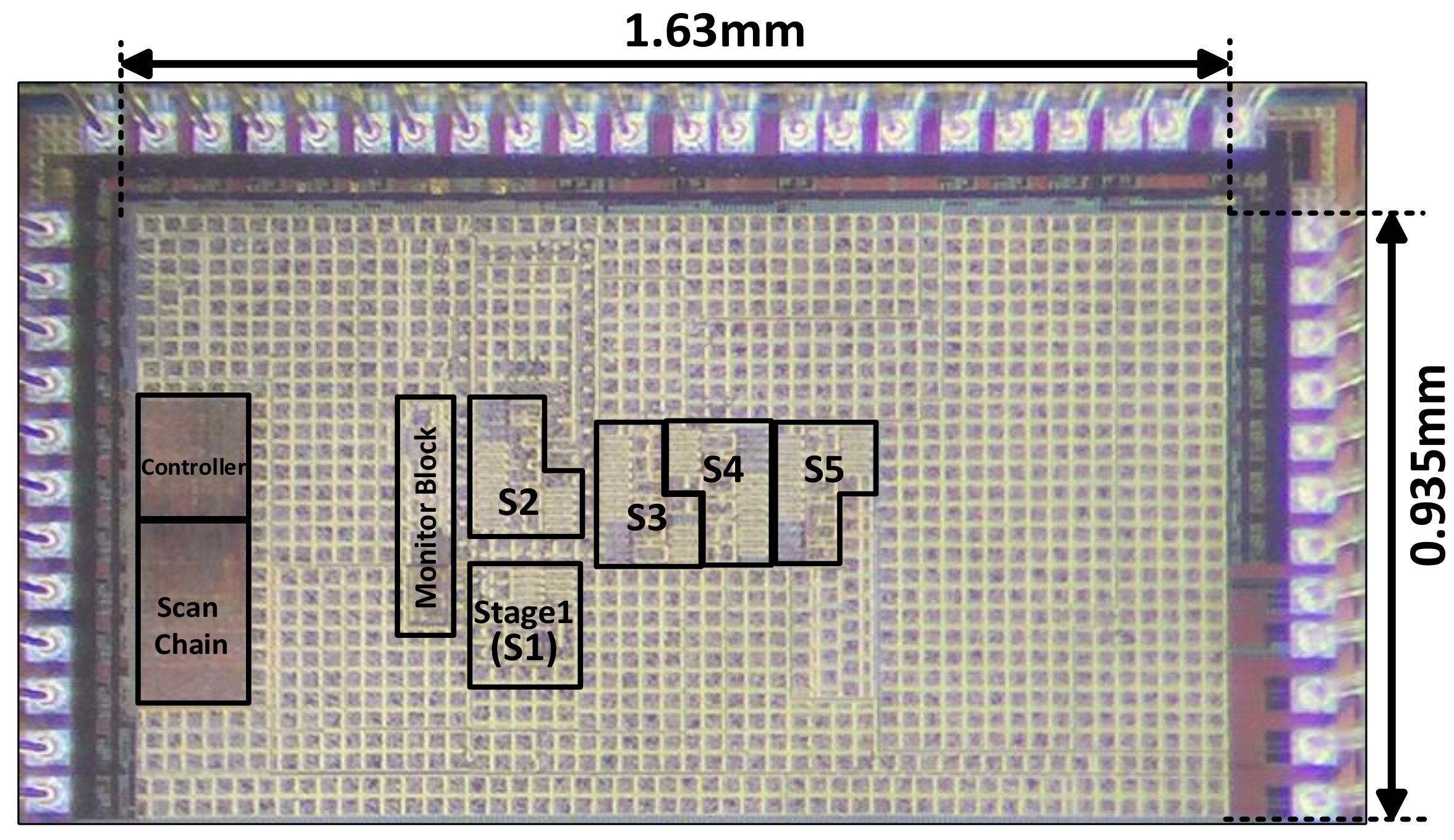
A prototype test chip was fabricated in a 180 nm complimentary metal-oxide-semiconductor (CMOS) process. An effective die area of 1.525 mm2 was utilized by the converter, which is dominantly occupied by 2.09 nF of on-chip MIM capacitors. The micrograph for the fabricated test chip is presented in Figure 17.
The prototype SC converter was examined over a wide load current and voltage range. The experimental results presented in Figure 18 and Figure 19 illustrate the importance of switch width modulation using multi-leaf structure under light load conditions. In these figures, the load current is fixed, and the operation frequency is swept for each conversion ratio configuration to measure the corresponding output voltage and efficiency. Colored curves represent the efficiency trend for configurations whose efficiency is the highest at least for one output voltage. Gray curves represent efficiency trends for configurations whose efficiency is never the optimal at any given output voltage and hence can be ignored. Under a light load (500 nA), minimum activation of switches is desired to minimize switching loss. Therefore, enabling only the smallest leaf is optimal (Figure 18a) and delivers output with approximately 13–20% higher efficiency compared with enabling all of the leaves (Figure 18b). However, under a higher load of 5 µA, two leaves are required to be activated to achieve comparable efficiency (Figure 19a) since enabling only the smallest leaf now incurs significant conduction loss. If too many leaves are activated, the efficiency drops again due to a large switching loss, as shown in Figure 19b, where all leaves are activated.
The effectiveness of switch width modulation by using multiple leaf structures is summarized in Figure 20, where 
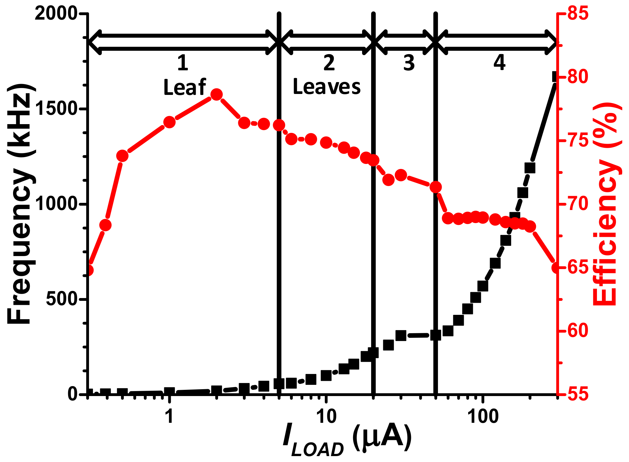
VOUT = 1.2 V is generated from VBAT = 4.0 V. For each load current point ranging from 300 nA to 300 µA (1000×), the optimal conversion ratio, operating frequency and number of active leaves are selected, and the corresponding efficiency and operating frequency are plotted. As load current increases, the optimal operating frequency also increases, and additional leaves should be gradually added to compensate for the increasing conduction loss.
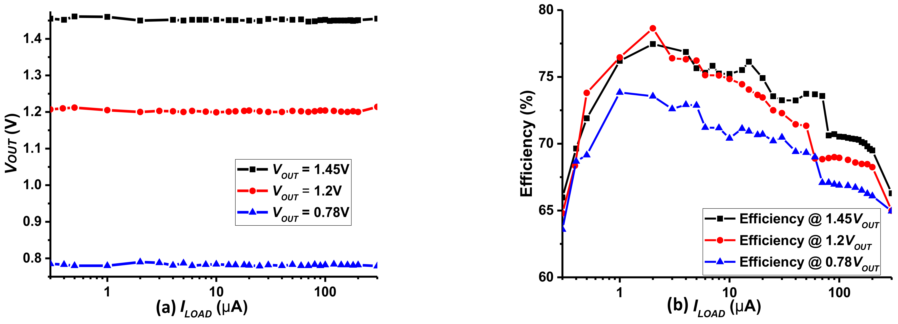
Figure 21a shows the experimental results for regulated output voltage levels when targeted for 0.78 V, 1.2 V, and 1.45 V with load current ranging from 300 nA to 300 µA. The optimal configuration is identified and measured for each load current point. The maximum regulation error was kept under ±16 mV thanks to the fine resolution provided with multi-ratio multi-stage topology. Figure 21b shows the corresponding efficiency trends. The proposed SC converter could operate with peak efficiencies of 73.9%, 77.96%, and 77.5% and minimum efficiencies of 63.58%, 64.79%, and 65.98% for target output voltages of 0.78 V, 1.2 V, and 1.45 V, respectively.
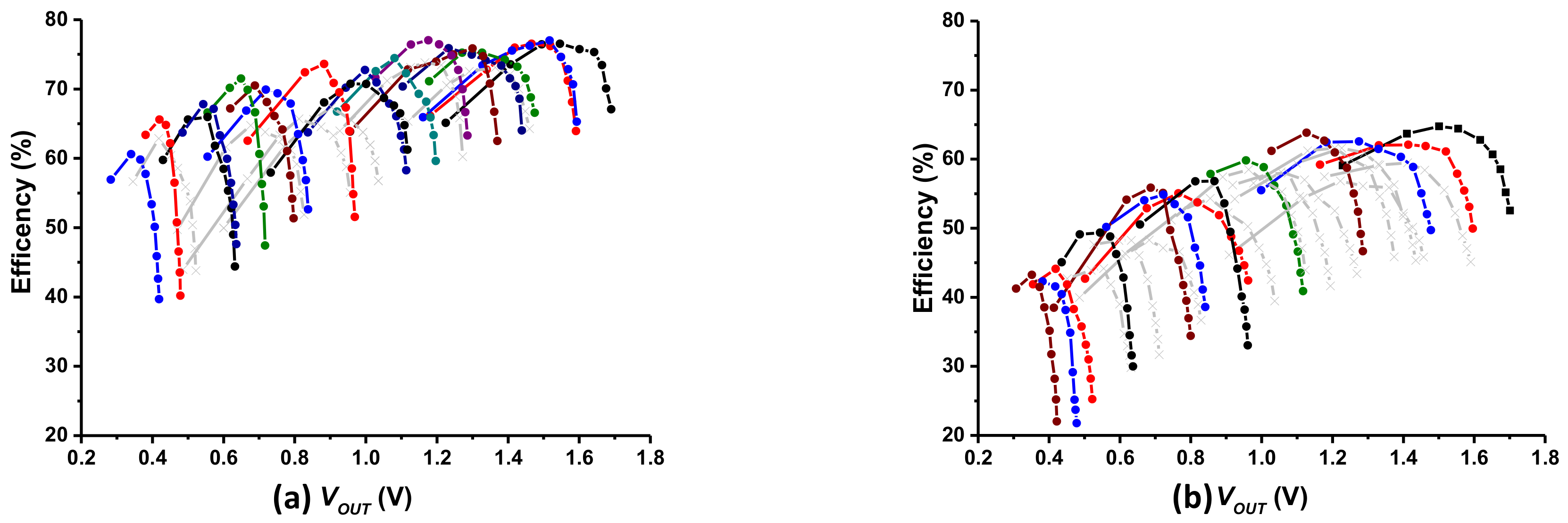
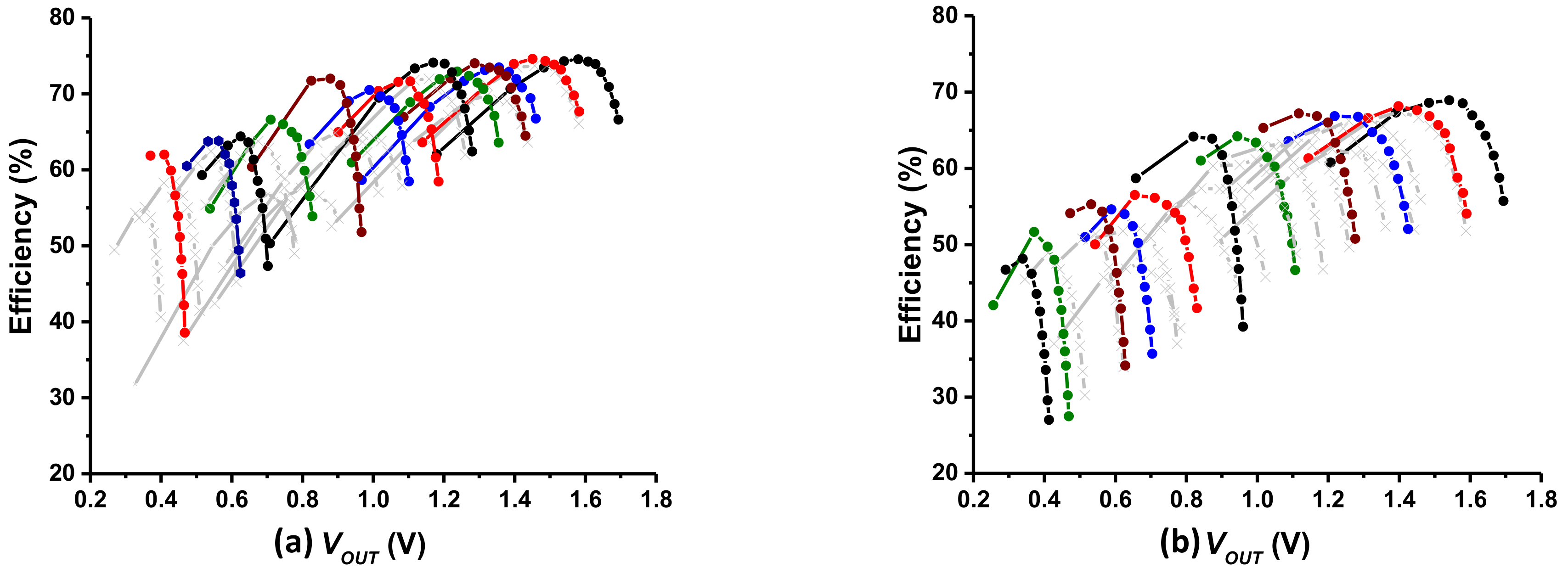
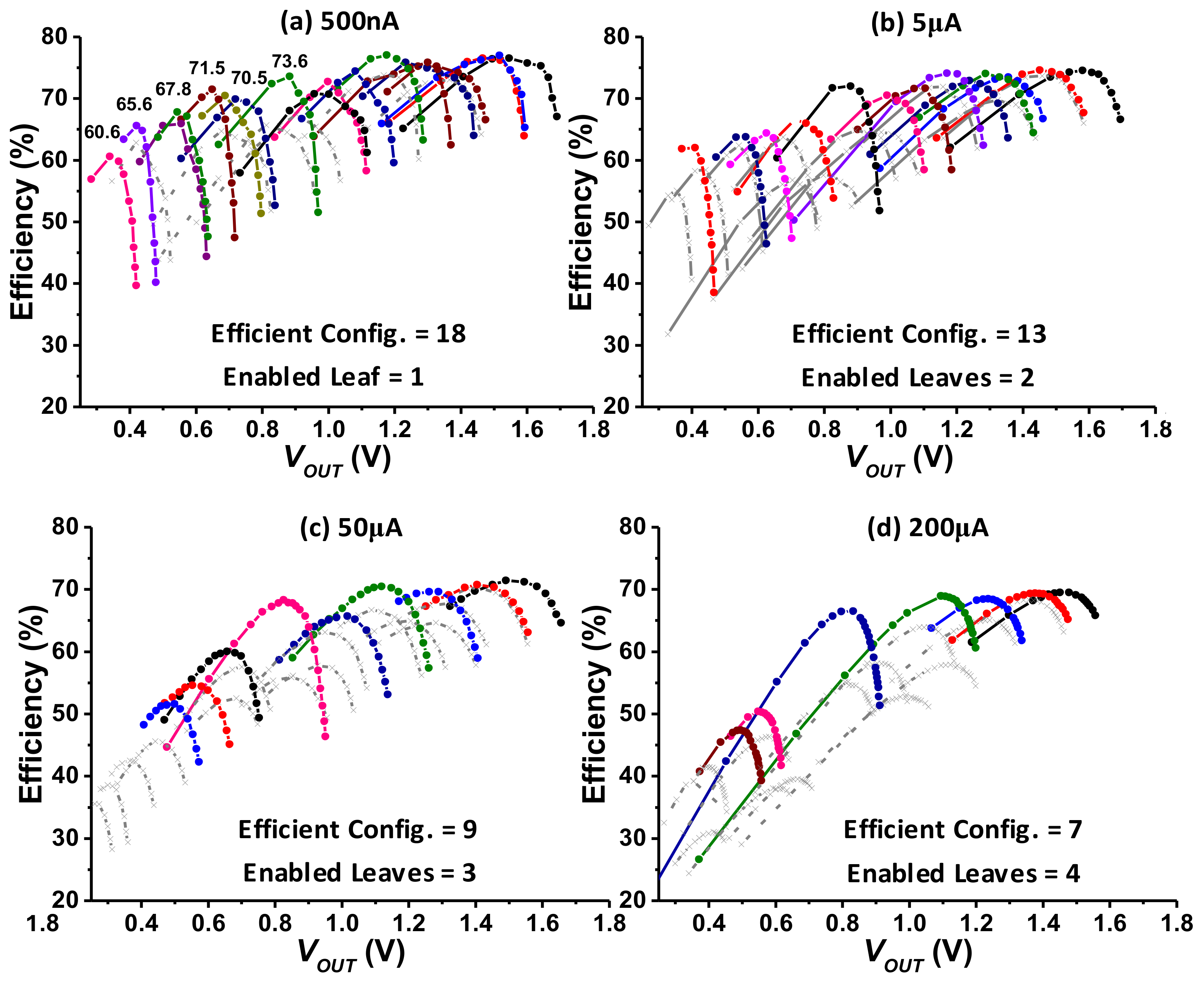
To verify the effectiveness of the proposed SC converter in providing dynamic voltage scalability in miniature sensors, the efficiency was measured over a target output voltage range of 0.4–1.6 V under various load conditions. The efficiency plots in Figure 22 show the efficiency trend for each conversion ratio configuration. The same color/grey notation in Figure 18 and Figure 19 is used in these plots.
Under the light load condition of 500 nA, each configuration is only effective for a narrow output voltage range, resulting in narrow efficiency curves. This implies that many conversion ratio configurations are required to maintain high efficiency over a wide DVS range, validating the loss analysis discussion presented in Section 2. With the fine voltage resolution, 18 configurations were required to keep conversion efficiency above 60% for the target voltage range, and the peak efficiency was >77% at VOUT of 1.176 V and 1.517 V. Only the smallest leaf was enabled to deal with the light load. Efficient operation under such light load conditions is essential for efficient miniature system operation during typically long standby.
When the load current is increased to 5 µA, the efficiency curves become slightly wider, and the number of required ratio configurations is reduced to 13. A second binary sized leaf is enabled to balance conduction and switching losses. The minimum efficiency for the entire output range was 62%, and the peak efficiency was 74.1%, as shown in Figure 22b.
As the load is further increased to 50 µA, three leaves need to be activated. Since the efficiency curves become even wider, fewer conversion ratios are required. This means less cascaded stages are required, and more stages can be parallel-connected to improve efficiency. Such parallelism facilitates high efficiency at high output voltages. However, for low output voltages, where many cascaded stages are required to form small conversion ratios, efficiency drops due to increased conduction loss. For a miniature sensor system, this is not a critical drawback since digital circuits with DVS tend to operate at high voltage when there is large current demand, i.e., computation demand. As shown in Figure 22c, the proposed SC converter could operate with >64% efficiency for an output range of 0.7–1.6 V with 50 µA load. When the voltage drops to 0.4 V, the efficiency drops to 47%, which is still high compared with the state-of-the-art systems [20,21] thanks to multi-leaves stage structure, stage configurability and cascading SC stages or parallel interconnect control.
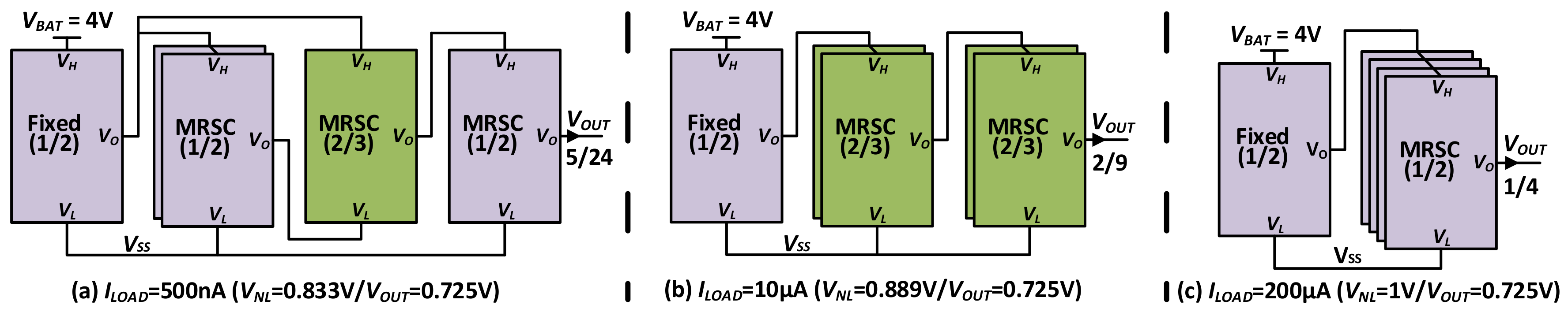
With a heavy load current of 200 µA, all available leaves are activated, and only a few configurations inheriting parallel interconnection of SC stages are used to cover the entire output range, as shown in Figure 22d. From the detailed efficiency trend analysis for wide load current and voltage ranges, the observation made earlier in the loss analysis section that, “cascading SC stages are required for efficient operation under light loads, whereas parallelism is required for heavy loads” is confirmed.
A performance comparison of the proposed architecture with state-of-the-art structures including successive approximation (SAR) [20], recursive tertiary (RTC) [21], and recursive binary (RBC) [22] converters is summarized in Table 4. The proposed SC converter provides finer 16 mV effective voltage resolution as compared to the SAR with fewer stages, resulting in more efficient operation by limiting conduction loss. The peak efficiency of the proposed converter is lower than recursive architectures (RTC, RBC), but finer granularity and VIN independent driving scheme results in significant efficiency improvement for light load conditions, which is crucial for duty-cycled miniature sensor systems. The proposed converter maintains efficient operation for very low output voltages even at higher VIN level, which is the major contribution of this work. Other SC converters in [15,16,17] are efficient SC converter designs but are based upon a single SC stage. Therefore, only few conversion ratios can be provided, making them unsuitable for DVS implementation.

5. Conclusions

A fully integrated SC converter is proposed for DVS implementation in ultra-low power miniature sensor systems. For efficient DVS operation, the SC converter should be able to efficiently provide a wide range of output voltage over a wide range of load current to handle both standby and active mode operation. With light load current, an SC converter configured for a given ratio can operate efficiently only within a narrow voltage range. Therefore, multi-ratio, multi-stage architecture with RSI was utilized for the proposed SC converter to provide numerous conversion ratios and hence fine voltage resolution. Switch width modulation using binary sized leaves was also implemented to balance switching and conduction losses over wide load ranges. A limited-swing switch-driving scheme allowed conversion from higher voltage battery without increase in switching overhead. RSI also enabled parallel connection of stages so that efficiency at heavy load could be improved by increasing the effective stage capacitance and switch size, reducing conduction loss.
The experimental results verify that the proposed SC converter operates with greater than 64% efficiency for load currents ranging from 300 nA to 300 µA (1000×) with 1.2 V, and greater than 48% efficiency at ultra-light load and low voltage conditions of 300 nA/0.4 V. Amongst all prior architectures, ref. [20] provides a maximum load current range of 1 µA to 300 µA (300×). Thus, the proposed SC converter not only provides efficient operation at different loading and voltage levels during active mode but also maintains efficient operation during standby mode, which can be the dominant operation mode in miniature systems. We believe this efficient SC converter enables efficient implementation of DVS, which can lead to significant improvement in battery lifetime for miniature systems.

Author Contributions

Y.L. (Yoonmyung Lee) guided and directed the authors for this work. H.S. proposed and designed the overall architecture of proposed SC converter and wrote the paper. Y.L. (Yongmin Lee), H.L., M.K., and M.B.K. contributed in prototype test chip design and layout. J.-H.C. advised on concept development and helped in writing the paper.

Funding

This work was supported by the Basic Research Lab Program through the National Research Foundation of Korea (NRF) funded by the Ministry of Science and ICT (2017R1A4A1015400) and ‘the Competency Development Program for Industry Specialists’ of the Korean Ministry of Trade, Industry and Energy (MOTIE), operated by Korea Institute for Advancement of Technology (KIAT) (No. N0001883, HRD program for Intelligent Semiconductor Industry). The EDA tool was supported by the IC Design Education Center (IDEC), Korea.

Conflicts of Interest

The authors declare no conflict of interest.

References

  1. Jang, T.; Kim, G.; Kempke, B.; Henry, M.B.; Chiotellis, N.; Pfeiffer, C.; Kim, D.; Kim, Y.; Foo, Z.; Kim, H.; et al. Circuit and System Designs of Ultra-Low Power Sensor Nodes with Illustration in a Miniaturized GNSS Logger for Position Tracking: Part II—Data Communication, Energy Harvesting, Power Management, and Digital Circuits. IEEE Trans. Circuits Syst. I 2017, 64, 2250–2262. [Google Scholar] [CrossRef]
  2. Kim, G.; Lee, Y.; Foo, Z.; Pannuto, P.; Kuo, Y.-S.; Kempke, B.; Ghaed, M.H.; Bang, S.; Lee, I.; Kim, Y.; et al. A Millimeter-Scale Wireless Imaging System with Continuous Motion Detection and Energy Harvesting. In Proceedings of the IEEE Symposium on VLSI, Honolulu, HI, USA, 178–17., 10–13 June 2014. [Google Scholar]
  3. Huang, K.K.; Brown, J.K.; Ansari, E.; Rogel, R.R.; Lee, Y.; Kim, H.; Wentzloff, D.D. An Ultra-Low-Power 9.8GHz Crystal-Less UWB Transceiver with Digital Baseband Integrated in 0.18 μm BiCMOS. IEEE J. Solid-State Circuits 2013, 48, 3178–3189. [Google Scholar] [CrossRef]
  4. Fabio, V. Comparison Among Different Rainfall Energy Harvesting Structures. Appl. Sci. 2018, 8, 955. [Google Scholar] [CrossRef]
  5. Craig, K.; Shakhsheer, Y.; Khanna, S.; Lach, J.; Calhoun, B.H. A 32b 90 nm Processor Implementing Panoptic DVS Achieving Energy Efficient Operation From Sub-Threshold to High Performance. IEEE J. Solid-State Circuits 2014, 49, 545–552. [Google Scholar] [CrossRef]
  6. Sturcken, N.; Petracca, M.; Warren, M.; Mantovani, P.; Carloni, L.P.; Peterchev, A.V.; Shepard, K.L. A switched-inductor integrated voltage regulator with nonlinear feedback and network-on-chip load in 45 nm SOI. IEEE J. Solid-State Circuits 2012, 47, 1935–1945. [Google Scholar] [CrossRef]
  7. Li, P.; Xue, L.; Hazucha, P.; Karnik, T.; Bashirullah, R. A delay-locked loop synchronization scheme for high-frequency multiphase hysteretic DC-DC converters. IEEE J. Solid-State Circuits 2009, 44, 3131–3145. [Google Scholar] [CrossRef]
  8. Nga, T.T.K.; Park, S.M.; Park, Y.-J.; Park, S.H.; Kim, S.; Thuong, T.V.C.; Lee, M.; Hwang, K.C.; Lee, K.-Y. A Wide Input Range Buck-Boost DC–DC Converter Using Hysteresis Triple-Mode Control Technique with Peak Efficiency of 94.8% for RF Energy Harvesting Applications. Energies 2018, 11, 1618. [Google Scholar] [CrossRef]
  9. Wen, M.; Steyaert, M.S.J. A fully integrated CMOS 800-mW four-phase semiconstant ON/OFF-time step-down converter. IEEE Trans. Power Electron. 2011, 26, 326–333. [Google Scholar]
  10. Kim, W.; Brooks, D.; Wei, G.-Y. A fully-integrated 3-level DC-DC converter for nanosecond-scale DVSF. IEEE J. Solid-State Circuits 2012, 47, 206–219. [Google Scholar] [CrossRef]
  11. Huang, C.; Mok, P.K.T. A 100 MHz 82.4% Efficiency Package-Bondwire Based Four-Phase Fully-Integrated Buck Converter With Flying Capacitor for Area Reduction. IEEE J. Solid-State Circuits 2013, 48, 2977–2988. [Google Scholar] [CrossRef]
  12. Keikhosravy, K.; Mirabbasi, S. A 0.13-μm CMOS Low-Power Capacitor-Less LDO Regulator Using Bulk-Modulation Technique. IEEE Trans. Circuits Syst. I 2014, 61, 3105–3114. [Google Scholar] [CrossRef]
  13. Shirmohammadli, V.; Saberkari, A.; Martinez-Garcia, H.; Alarcon-Cot, E. Low Power Output-Capacitorless class-AB CMOS LDO Regulator. In Proceedings of the IEEE International Symposium on Circuit and Systems (ISCAS), Baltimore, MD, USA, 28–31 May 2017. [Google Scholar] [CrossRef]
  14. Khan, Z.H.N.; Park, Y.-J.; Oh, S.J.; Jang, B.G.; Park, S.-M.; Abbasizadeh, H.; Pu, Y.G.; Hwang, K.C.; Yang, Y.; Lee, M.; et al. Design of Peak Efficiency of 85.3% WPC/PMA Wireless Power Receiver Using Synchronous Active Rectifier and Multi Feedback Low-Dropout Regulator. Energies 2018, 11, 479. [Google Scholar] [CrossRef]
  15. El-Damak, D.; Bandyopandhyay, S.; Chandrakasan, A.P. A 93% Efficiency Reconfigurable Switched-Capacitor DC-DC Converter Using On-Chip Ferroelectric Capacitors. In Proceedings of the IEEE International Solid State Circuits Conference (ISSCC), San Francisco, CA, USA, 17–21 February 2013; pp. 374–375. [Google Scholar]
  16. Ramadass, Y.K.; Chandrakasan, A.P. Voltage scalable switched capacitor DC–DC converter for ultra-low-power on-chip applications. In Proceedings of the 2007 IEEE Power Electronics Specialists Conference, FL, USA, 17–21 June 2007; pp. 2353–2359. [Google Scholar]
  17. Ramadass, Y.K.; Fayed, A.A.; Chandrakasan, A.P. A fully-integrated switched-capacitor step-down DC–DC converter with digital capacitance modulation in 45 nm CMOS. IEEE J. Solid-State Circuits 2010, 45, 2557–2565. [Google Scholar] [CrossRef]
  18. Le, H.P.; Crossley, J.; Sanders, S.R.; Alon, E. A sub-ns response fully integrated battery-connected switched-capacitor voltage regulator delivering 0. In 19W/mm2 at 73% efficiency. In Proceedings of the IEEE International Solid State Circuits Conference (ISSCC), San Francisco, CA, USA, 17–21 February 2013; pp. 372–373. [Google Scholar]
  19. Ozaki, T.; Hirose, T.; Asano, H.; Kuroki, N.; Numa, M. A 0.38-μW stand-by power, 50-nA-to-1-mA load current range DC-DC converter with self-biased linear regulator for ultra-low power battery management. In Proceedings of the IEEE Asian Solid State Circuits Conference (A-SSCC), Toyama, Japan, 7–9 November 2016; pp. 225–228. [Google Scholar]
  20. Bang, S.; Blaauw, D.; Sylvester, D. A Successive-Approximation Switched-Capacitor DC–DC Converter with Resolution of VIN/2N for a Wide Range of Input and Output Voltages. IEEE J. Solid-State Circuits 2016, 51, 543–556. [Google Scholar]
  21. Salem, L.G.; Mercier, P.P. A 45-ratio recursively sliced series-parallel switched-capacitor DC–DC converter achieving 86% efficiency. In Proceedings of the IEEE Custom Integrated Circuits Conference (CICC), San Jose, CA, USA, 15–17 September 2014. [Google Scholar] [CrossRef]
  22. Salem, L.G.; Mercier, P.P. A recursive switched capacitor DC–DC converter achieving ratios with high efficiency over a wide output voltage range. IEEE J. Solid-State Circuits 2014, 49, 2773–2787. [Google Scholar] [CrossRef]
  23. Saif, H.; Lee, Y.; Kim, M.; Lee, H.; Khan, M.B.; Lee, Y. A wide load and voltage range switched-capacitor DC-DC converter with load-dependent configurability for DVS implementation in miniature sensors. In Proceedings of the IEEE Asian Solid State Circ. Conference (A-SSCC), Seoul South Korea, 6–8 November 2017; pp. 125–128. [Google Scholar]
  24. Saponara, S.; Ciarpi, G. IC Design and Measurement of an Inductor less 48 V DC/DC Converter in Low-Cost CMOS Technology Facing Harsh Environments. IEEE Trans. Circuits Syst. I 2018, 65, 380–393. [Google Scholar] [CrossRef]
  25. Bhargava, A.; Pommerenke, D.; Kam, K.W.; Centola, F.; Lam, C.W. DC-DC Buck Converter EMI Reduction Using PCB Layout Modification. IEEE Trans. Electromagn. Compat. 2011, 53, 806–813. [Google Scholar] [CrossRef]
  26. Saponara, S.; Ciarpi, G.; Groza, V.Z. Design and experimental measurement of EMI reduction techniques for integrated switching DC/DC Converters. IEEE Can. J. Electr. Comput. Eng. 2017, 40, 116–127. [Google Scholar]
  27. Le, H.P.; Sanders, S.R.; Alon, E. Design Technique for fully integrated Switched-Capacitor DC-DC Converters. IEEE J. Solid-State Circuits 2011, 46, 2120–2131. [Google Scholar] [CrossRef]
  28. Seeman, M.D.; Sanders, S.R. Analysis and optimization of switched-capacitor DC-DC converters. IEEE Trans. Power Electron. 2008, 23, 841–851. [Google Scholar] [CrossRef]
  29. Meyvaert, H.; Pique, G.V.; Karadi, R.; Bergveld, H.J.; Steyaert, M.S.J. A Light-Load-Efficient 11/1 Switched-Capacitor DC-DC Converter With 94.7% Efficiency While Delivering 100 mW at 3.3 V. IEEE J. Solid-State Circuits 2015, 50, 2849–2859. [Google Scholar] [CrossRef]
  30. Jung, W.; Oh, S.; Bang, S.; Lee, Y.; Foo, Z.; Kim, G.; Zhang, Y.; Sylvester, D.; Blaauw, D. An Ultra-Low Power Fully Integrated Energy Harvester Based on Self-Oscillating Switched-Capacitor Voltage Doubler. IEEE J. Solid-State Circuits 2014, 49, 2800–2811. [Google Scholar] [CrossRef]
  31. Fojtik, M.; Kim, D.; Chen, G.; Lin, Y.-S.; Fick, D.; Park, J.; Seok, M.; Chen, M.-T.; Foo, Z.; Blaauw, D.; et al. A Millimeter-Scale Energy-Autonomous Sensor System with Stacked Battery and Solar Cells. IEEE J. Solid-State Circuits 2014, 48, 801–813. [Google Scholar] [CrossRef]
Figure 1. A 2-phase 2:1 step down switched capacitor (SC) converter.
Energies 11 03092 g001
Figure 2. Loss contribution in single stage 2:1 SC converter from VIN = 2.0 V (a) Light load (500 nA). (b) Heavy load (100 μA).
Energies 11 03092 g002
Figure 3. Efficiency of the 2:1 SC converter at varying load.
Energies 11 03092 g003
Figure 4. Effect of switch width modulation using leaf enable mechanism on efficiency of 2:1 converter at ILOAD = 500 nA.
Energies 11 03092 g004
Figure 5. Effect of gate drive voltage swing variation VIN = 2.0 V (a) Light load (500 nA). (b) Heavy load (100 μA).
Energies 11 03092 g005
Figure 6. Multistage converter (a) Proposed reconfigurable SC topology. (b) Series connected. (c) Parallel connected.
Energies 11 03092 g006
Figure 7. Multi-ratio, multi-leaf SC converter stage.
Energies 11 03092 g007
Figure 8. Multi-ratio, multi-leaf SC converter stage structure (a) Simplified diagram. (b) Operation scheme for 1/2 ratio. (c) 1/3 ratio. (d) 2/3 ratio.
Energies 11 03092 g008
Figure 9. Switch level implementation of the Reconfigurable Stage Interconnection (RSI) scheme.
Energies 11 03092 g009
Figure 10. Three possible stage interconnect operation modes: (a) AnBn = 00. (b) AnBn = 01. (c) AnBn = 1X.
Energies 11 03092 g010
Figure 11. Operation of reconfigurable SC converter at no load (a) VOUT = 1.148 V. (b) VOUT = 1.167 V.
Energies 11 03092 g011
Figure 12. Optimal configuration for various load conditions when target VOUT = 0.725 V from VBAT = 4.0 V.
Energies 11 03092 g012
Figure 13. Cross coupled level shifter for gate diving (a) P-type level shifter (PLS). (b) N-type level shifter (NLS). (c) N-type level shifter operation.
Energies 11 03092 g013
Figure 14. Leakage-controlled delay cell (a) Conventional single branch. (b) Modified two leakage control Branches.
Energies 11 03092 g014
Figure 15. (a) Block diagram of leakage-based clock generator. (b) Frequency vs. control voltage (VCONT).
Energies 11 03092 g015
Figure 16. Reference comparison circuit for leaf control with VCONT.
Energies 11 03092 g016
Figure 17. Chip micrograph.
Energies 11 03092 g017
Figure 18. Efficiency vs. VOUT at ILOAD = 500 nA (a) Only 1 (smallest) leaf enable (Min. switch size). (b) All leaves enabled (Max. switch size).
Energies 11 03092 g018
Figure 19. Efficiency vs. VOUT at ILOAD = 5 µA (a) Leaf 1 and 2 enabled. (b) All leaves enabled (Max. switch size).
Energies 11 03092 g019
Figure 20. Frequency, efficiency and active leaves vs. ILOAD.
Energies 11 03092 g020
Figure 21. (a) Regulated output voltage vs. ILOAD. (b) Corresponding efficiencies.
Energies 11 03092 g021
Figure 22. Multi-ratio, multi-leaf SC converter’s efficiency curves at ILOAD (a) 500 nA. (b) 5 µA. (c) 50 µA. (d) 200 µA.
Energies 11 03092 g022
Table 1. Parameters summary.
AbbreviationDescriptionUnit
ΔVRipple voltagemV
ILOADLoad currentA
fSWSwitching frequencyHz
CFLYFlying capacitors capacitanceF
KCRipple conduction loss coefficientConstant
RONSwitch resistance per unit widthΩ·m
KSWSwitch resistance conduction loss coefficientConstant
WSWTotal width of switchesm
KPCapacitor parasitic loss coefficientConstant
VOUTOutput voltageV
CPFlying capacitors bottom plate parasitic capacitanceF
VSWGate drive voltage swingV
CGateNet switch gate capacitanceF
VdropVoltage deviation from ideal no load voltageV
KLNet loss coefficientConstant
Table 2. Switching sequence.
RatioEN1/3EN2/3Enabled (Φ1 or Φ2)Disabled (Always off)Φ1Φ2
1/2001,2,3,4,9,10,11,125, 6, 7, 81, 3, 10, 122, 4, 9, 11
1/3101,3,4,5,6,10,11,122, 7, 8, 91, 3, 10, 124, 5, 6, 11
2/3011,2,4,7,8,9,10,113, 5, 6, 121, 7, 8, 102, 4, 9, 11
Table 3. Reconfigurable stage interconnect (RSI) control bits.
Control BitsVH(n)VL(n)VS(n)
AnBn
00VS(n−1)VSSVS(n1)
01½VBATVS(n1)VS(n1)
1XVH(n−1)VL(n1)=VS(n1) (parallel)
Table 4. Performance comparison with prior SC down-converters.
ParametersThis Work[20][21][22][15][16][17]
TopologyReconfigurable Multi-StageSuccessive ApproximationRecursive TertiaryRecursive BinarySingle Stage ReconfigurableVoltage ScalableSingle Ratio SC
Technology180n180n250n250n130n180n45n
VIN(V)43.4–4.32.52.51.51.21.8
VOUT(V)0.4–1.6>0.450.1–2.240.1–2.20.4–1.10.3–1.10.8–1
Number of Conversion Ratios75 for 0.4 V–1.6 V
250 for 0 V–4.0 V
(VBAT = 4.0 V)
20 for 0.9 V–1.5 V
128 for 0 V–4.0 V
(VBAT = 4.0 V)
4515451
Voltage Step Resolution16 mV @ 4.0 VBAT31 mV @ 4.0 VBAT55 mV @ 2.5 VBAT167 mV @ 2.5 VBAT---
Number of Stages1 + 41 + 534111
Capacitor TypeMIM CapOn chipMIM CapMIM capFerroelectricGate OxideGate Oxide
Output Load Range300 nA–300 μA (1000×)1 μA–300 μA (300×)<1.86 mA<2 mA20 μA–1 mA (50×)5 μW–1 mW
(200×)
100 μA–8 mA (80×)
Capacitance2.09 nF2.24 nF2.8 nF3 nF8 nF2.4 nF1.234 nF
Frequency2 k–2.3 M80 k–2.7 M---<15 M<30 M
Area (mm²)1.5251.694.34.6450.3660.570.16
ηMAX (%)7772868593~7769
η @ Heavy Load69% @ 300 μA
(1.2 V)
(ratio = 3/10)
54% @ 300 μA
(1.2 V)
(ratio = 3/10)
74% @ 1.86 mA (1.2 V)
(ratio = 4.8/10)
73% @ 2 mA (1.2 V)
(ratio=4.8/10)
93% @ 500 μA (0.96 V)
(ratio = 6.4/10)
73% @ 100 μW (0.8 V)
(ratio = 2/3)
65% @ 8 mA @ (0.90 V)
(ratio = 1/2)
η @ Light Load76% @ 500 nA (1.2 V)
64% @ 300 nA (1.2 V)
64% @ 4 μA (1.2 V)--73% @ 20 μA (0.96 V)-48% @ 100 μA (0.90 V)
η @ Light Load & Low Voltage64% @ 500 nA (0.4 V)
48% @ 300 nA (0.4 V)
45% @ 2 μA (0.9 V)---74% @ 5 μW
@ 0.5 V
-

