Slope Compensation Design for a Peak Current-Mode Controlled Boost-Flyback Converter

1
Departamento de Ingeniería Eléctrica, Electrónica y Computación, Percepción y Control Inteligente, Facultad de Ingeniería y Arquitectura, Universidad Nacional de Colombia—Sede Manizales, Bloque Q, Campus La Nubia, Manizales 170003, Colombia
2
Departamento de Ingeniería Electrónica y Telecomunicaciones, Automática, Electrónica y Ciencias Computacionales (AE&CC), Instituto Tecnológico Metropolitano, Medellín 050013, Colombia
*
Author to whom correspondence should be addressed.
Energies 2018, 11(11), 3000; https://doi.org/10.3390/en11113000
Submission received: 27 September 2018
/
Revised: 28 October 2018
/
Accepted: 29 October 2018
/
Published: 1 November 2018
(This article belongs to the Special Issue Control and Nonlinear Dynamics on Energy Conversion Systems)
Abstract
:Peak current-mode control is widely used in power converters and involves the use of an external compensation ramp to suppress undesired behaviors and to enhance the stability range of the Period-1 orbit. A boost converter uses an analytical expression to find a compensation ramp; however, other more complex converters do not use such an expression, and the corresponding compensation ramp must be computed using complex mechanisms. A boost-flyback converter is a power converter with coupled inductors. In addition to its high efficiency and high voltage gains, this converter reduces voltage stress acting on semiconductor devices and thus offers many benefits as a converter. This paper presents an analytical expression for computing the value of a compensation ramp for a peak current-mode controlled boost-flyback converter using its simplified model. Formula results are compared to analytical results based on a monodromy matrix with numerical results using bifurcations diagrams and with experimental results using a lab prototype of 100 W.
1. Introduction
The main purpose of power converters is to change the level voltage. Currently, this task is achieved by controlling a converter through pulse width modulation (PWM) such that the system is described by a set of dynamic equations. Power converters can be modeled as a piecewise linear dynamic system [1,2,3], and all exhibit a plethora of nonlinear phenomena depending on the parameter values used. Such behaviors, which are currently being examined at length [4,5,6,7], include period-doubling bifurcations, subharmonics and chaos [2,8,9].
The main goal of a converter is usually to contribute a load with a desired voltage; in this sense, it is important to compute and analyze the stability of the Period-1 orbit and to study its complex dynamics (a complete revision of stability analysis methods applied to power converters can be found in [10]). The behaviors of a power converter are often determined by plotting bifurcation diagrams [4,5,11,12] using the Poincaré map [3]. In these diagrams, as a parameter value changes, the Poincaré map of the steady state is plotted. The stability of the Period-1 orbit is also analyzed by presenting the Poincaré map as a monodromy matrix such that by analyzing eigenvalues of the monodromy matrix (Floquet multipliers), it is possible to determine the stability of a Period-1 orbit [13]. Several studies also combine bifurcations and monodromy matrix analyses [6,14].
High step-up power converters are some of the main devices used in photovoltaic applications [15,16,17,18,19] due to the low output voltage of solar panels. With such applications, efficiency is a key issue, so single-stage converters are preferred over more complex converters [17,18]. Strong gains can be achieved through single-stage conversion by using coupled inductors where basic converters can be coupled, improving the advantages of every configuration to extend the voltage conversion ratio, suppress the switch voltage spike, recycle leakage energy and increase efficiency levels [17,18,20].
A converter that couples buck, boost and flyback topologies is presented in [17]. The converter consists of one MOSFET (metal-oxide-semiconductor field-effect transistor), four diodes, three inductors and three capacitors, rendering the system and controller difficult to model, analyze and design. This is the case due to the high-order dynamic equations used in the uncontrolled system (sixth order) and due to the number of electronic devices (five) used, which renders 32 topologies possible. A structure based on SEPIC (single-ended primary-inductor converter) and boost-flyback converters was proposed in [18]. This converter was composed of four semiconductors and eight energy storage elements. The system is difficult to use for analyses (eight differential equations and 16 topologies) and is less efficient than the converter presented in [17]. In a similar vein, a converter coupling several cells of flyback converters with switched capacitors was proposed in [16,21] Although this application considerably increases the voltage, the model is complex for the same reasons noted above, and its analysis and control design are difficult to use.
Because of the aforementioned drawbacks, researchers have returned to a more basic and efficient structure: the boost-flyback (BF) converter [22,23]. In a BF, boost and flyback converters are integrated via magnetic coupling between two inductors to form a BF converter to achieve a good trade-off between voltage gains, efficiency and complexity. Due to its high voltage gains, high efficiency and limited complexity relative to similar models, the boost-flyback converter is widely used in various applications such as in hybrid electric vehicles [24,25], for voltage balancing [26], in low-scale arrays of photovoltaic panels [27], in LED lighting [28,29] and for power factor correction [29]. A boost-flyback converter includes two capacitors, two coupled inductors, two diodes and one MOSFET such that the designer may use four differential equations and eight potential topologies. The efficiency and voltage gain were improved in [30,31], by adding other primary and secondary coils, leading to the same problems described above. In a similar way, the efficenciy was improved for gains greater than eight by adding switched coupled inductors, rendering the system more complex [32].
One of the most popular control techniques used in power converters is that of so-called peak current-mode control [33,34,35,36]. When the value of the slope is low, the system remains stable. As the duty cycle progresses, the system turns unstable, and when the slope value is very high, subharmonics are present [37,38], limiting the time response of the controlled system [39] and compromising performance [40]. In this way, it is necessary to find the correct compensation ramp value to avoid a fast scale related to the inner control loop [41,42] or a slow scale due to the outer control loop [43,44]. Both dynamic behaviors have been widely studied in reference to several converters [45,46,47,48]. Once slope compensation is designed, system behaviors can be improved by changing, retuning or controlling slope compensation. To improve the behavior of the controlled system, a polynomial curve slope compensation scheme was proposed [14]. This slope secures better results than a traditional linear ramp slope compensation scheme, though its practical implementation is less straightforward. The performance of current-mode control was optimized by means of an autotuning technique of the ramp slope, allowing for a broader control bandwidth than the traditional technique [49]. On the other hand, some peak current-mode control techniques avoid the use of an external signal generator alleviating the deviation of the inductor current peak value from its desired reference [10] and improving the range of the current reference [50].
In this paper, an analytical expression for determining the initial value of the slope compensation of a BF converter via peak current-mode control is determined. Unlike modern means of improving the range of stability of the compensation ramp [10,14,49,50], the proposed technique is less complex and therefore easier to implement and allows the precise calculation of the compensation ramp, which guarantees correct operation and prevents unwanted behaviors from manifesting. A complete analysis of stability and transitions to chaos for a peak-current mode-controlled BF converter is reported in [51], and the coexistence of Period-1, Period-2 and chaotic orbits with varying coupling coefficients has been proven via bifurcation analysis [52]. However, neither analytical expressions for computing the value of the compensation ramp of a peak-current controlled BF converter, nor experimental data that confirm the corresponding analytical expression have been even published.
An analytical expression is first obtained by simplifying the problem. Corresponding results are compared to those derived from three sources. (a) Results can first be derived from analytical expressions computed with a complete model and using the monodromy matrix [13]. In this case, the monodromy matrix is computed analytically, and its eigenvalues are calculated as the parameter varies. The largest absolute value of its eigenvalues is called the LAVE. (b) Numerical results can also be obtained from bifurcation diagrams computed by brute force and (c) from experiments carried out in a lab prototype of 100 W. All results show good agreement.
The rest of this paper is organized as follows. In Section 2, the operation mode of the boost-flyback converter is described, as well as that of peak-current mode control. In Section 3, computations for obtaining the mathematical expression for slope compensation are presented. In Section 4, numerical and experimental results are shown and compared. Numerical results are obtained using the derived formula for a particular converter using parameters similar to those used in the experimental setup, including the nonideal model (internal resistance for certain components). The experimental results are obtained from a 100-watt lab prototype and they are presented and compared to numerical ones. Finally, Section 5 concludes.
2. Boost-Flyback Converter: Modeling and Control
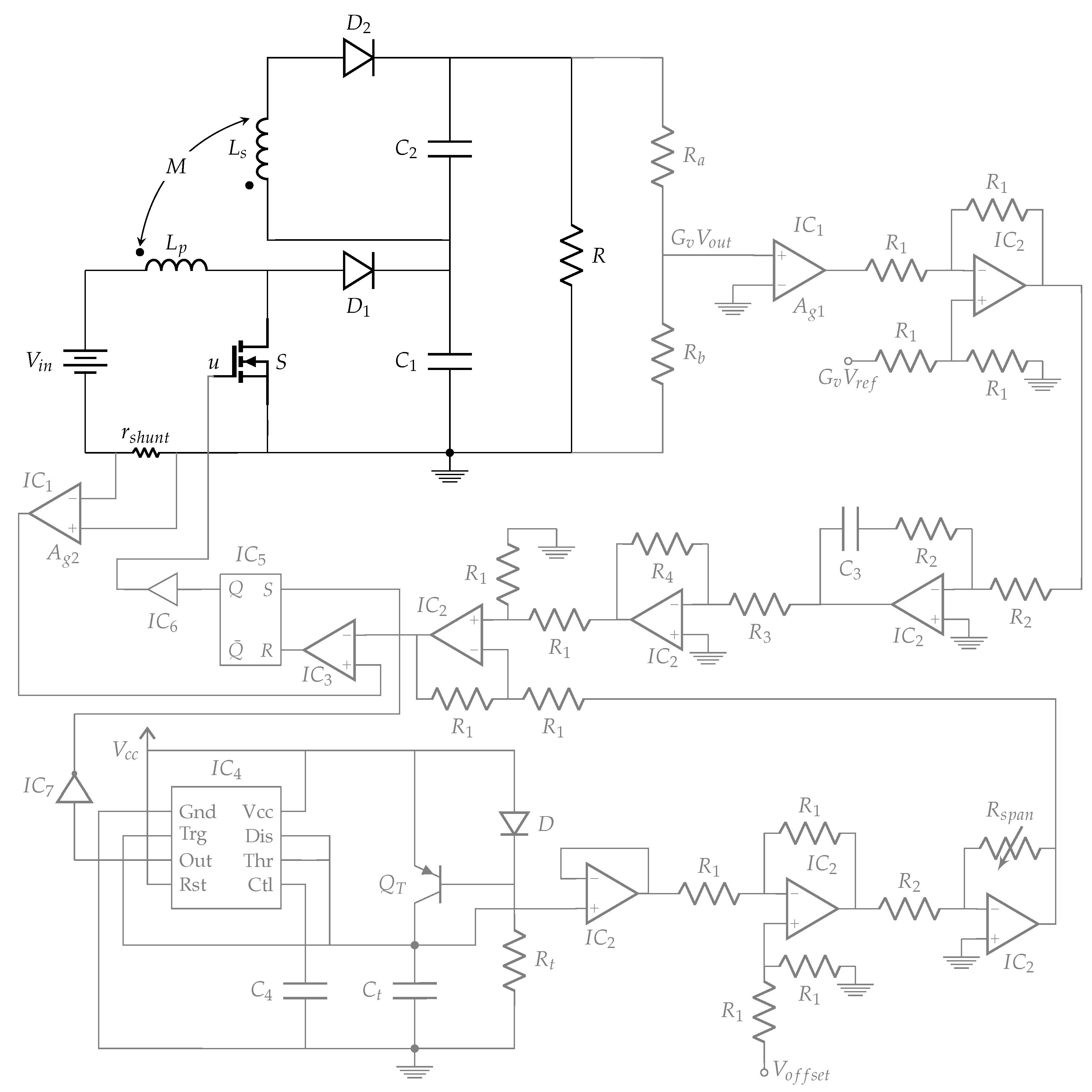
A peak-current controlled boost-flyback converter is depicted in Figure 1. The boost-flyback components are denoted with black lines while the controller is denoted with gray lines. The boost-flyback consists of two coupled inductors (, ), two capacitors (, ), one MOSFET (S) and two diodes (, ). The MOSFET is controlled while the diodes commutate depending on their degree of polarization. As the name implies, the union of a boost and flyback converter achieves high gains and high levels of efficiency, while the stress voltage of semiconductor devices decreases relative to that of a standard flyback [23,53].
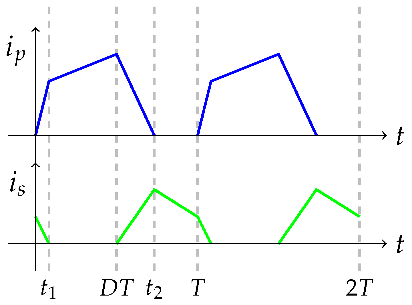
As three semiconductor devices are used, there are eight possible switch configurations or states: ... . However, it has been shown that only six states have physical meaning [54], and it has been also proven that the controlled system exhibits a Period-1 orbit switching between four states, as described in Table 1 [51]. A schematic diagram of the steady state current behavior of a Period-1 solution is presented in Figure 2. States and are present when the MOSFET is turned on, and states and are present when the MOSFET is turned off.
From , the system evolves as follows: . A change from to occurs when at ; the system switches from to when the switching condition is satisfied at , which is referred to as the duty cycle and which corresponds to the ratio between the time at which the MOSFET is turned on and the period T, i.e.,: ; changes to when (at ), and finally, when , the system returns to . The set of differential equations describing the Period-1 orbit is shown below:
State 1: , :
State 2: , :
State 3: , :
State 4: , :
where is the input voltage, and are the primary and secondary currents, respectively, and are the voltages across capacitors and and is the mutual inductance, with as the coupling coefficient and . The output voltage is .
Peak current-mode control is widely used for the control of power converters [41,47,51]. A general schematic diagram of the boost-flyback converter with the proposed controller is depicted in Figure 1. When peak current-mode control is used, a fixed switching frequency is obtained, and current behaviors are very similar to those shown in Figure 2. At the start of the period, the MOSFET is active, the current increases and the current declines to ; at time , dynamic equations describing the system change while the MOSFET continues on until is equal to the reference current at . At , switches stop until the next cycle begins. Signal is composed of two parts: the first (denoted as ) is provided by a PI controller applied to the output voltage error . The second part corresponds to the signal supplied by the compensation ramp . Thus, the reference current can be expressed as:
where and [A/(V.t)] are parameters associated with the PI controller and [A]corresponds to the amplitude of the compensation ramp. As a result of the controller, there is only one switching cycle per period. At the start of the period, the switch turns on, and it remains on until switching condition is achieved (the corresponding duty cycle). When , the switch opens and remains open until the next period starts. As sliding is not possible (i.e., there is only one round of commutation per cycle), the switching condition can be expressed as:
where is the duty cycle.
3. Slope Compensation Design
To our knowledge, the related literature has not reported on a means of determining the slope of the compensation ramp of a boost-flyback converter, which can be used to stabilize the Period-1 orbit. The objective of this section is to analyze the slopes of currents flowing through inductors to find an analytical expression to determine the slope of a compensation ramp and thus to guarantee the stability of the Period-1 orbit. Figure 3 presents the behavior of currents flowing through primary and secondary coils when the system operates within the Period-1 orbit described by states , , and . Slopes are clearly marked in the figure.
3.1. Assumptions
In the analysis, the following approximations are considered. (i) For all elements and devices, the internal resistances are zero. (ii) The steady-state output of the PI-controller () is constant, and hence, its derivative is zero. However, as can be seen in the procedure, the constant value is not needed to compute the final expression. (iii) Voltages and are constant and can be computed as a function of the duty cycle D; is the output of the boost component, and is the output of the flyback component, taking into account the coupling factor (see Appendix A for a complete derivation of the formula.
(iv) Finally, all currents can be mathematically expressed as straight lines such that slopes associated with include , and , while slopes associated with include , and (see Figure 3). These slopes can be computed from Equations (2)–(5) as follows:
In a similar way as the slope compensation in a boost power converter is designed considering the stability of the Period-1 orbit [33], in this paper, we present an analysis of the stability of the Period-1 orbit based on information on current slopes and on conditions that should be met to guarantee the stability of the controlled system. To analyze the stability of the Period-1 orbit, small perturbations are applied at the beginning of the cycle, and its corresponding value is measured at the end of period T. When the magnitude of perturbation increases, the Period-1 orbit is unstable; by contrast, when the magnitude of perturbation decreases, the orbit is stable.
3.2. Mathematical Procedure
3.2.1. Analysis of Currents in the Primary Coil
At switching time , a pair of equations is fulfilled in Figure 3: one to its left and the other to its right. When defining the slope of the compensation ramp as , at the switching time, the following equation is satisfied:
Based on perturbation observed in the initial condition, the last equation can be expressed as follows:
From (11),
In a similar way, the analysis illustrated to the right of the switching time leads to the following equation.
Taking into account the perturbation, this equation is given by:
From (15),
3.2.2. Analysis of Currents in the Secondary Coil
Now, the expressions for the current and its perturbation are computed. At , they are as follows:
and:
From this equation, can be expressed as:
Now, at , the following equation is fulfilled,
At the same time , the perturbed equation is:
3.2.3. Stability Condition
Then, the stability of the Period-1 orbit is given by the absolute value of . When , the periodic orbit is unstable; when , it is asymptotically stable; and when , it corresponds to the limit of stability. To guarantee that the system operates within a Period-1 orbit, the slope of the compensation ramp must satisfy the following expression:
4. Results
Parameters associated with the converter and experiment are presented in Table 2. The first two columns are needed to simulate the system, and the other parameters describe the electronic circuit.
4.1. Numerical Results
To compare the results obtained using Equation (28) with the analytical results, we determined the stability of the Period-1 orbit from the saltation matrix associated with switching times [13,55,56]. A complete analysis of the stability and computation of the saltation matrix for this system can be found in [51]. Parameter values used for the simulations and experiments are given in Table 2. Voltages and are computed from Equation (7); the slopes of straight lines are calculated from Equation (8); and the output voltage corresponds to the desired output voltage and . With these data, the desired output voltage varies, and the limit value of slope compensation is obtained.
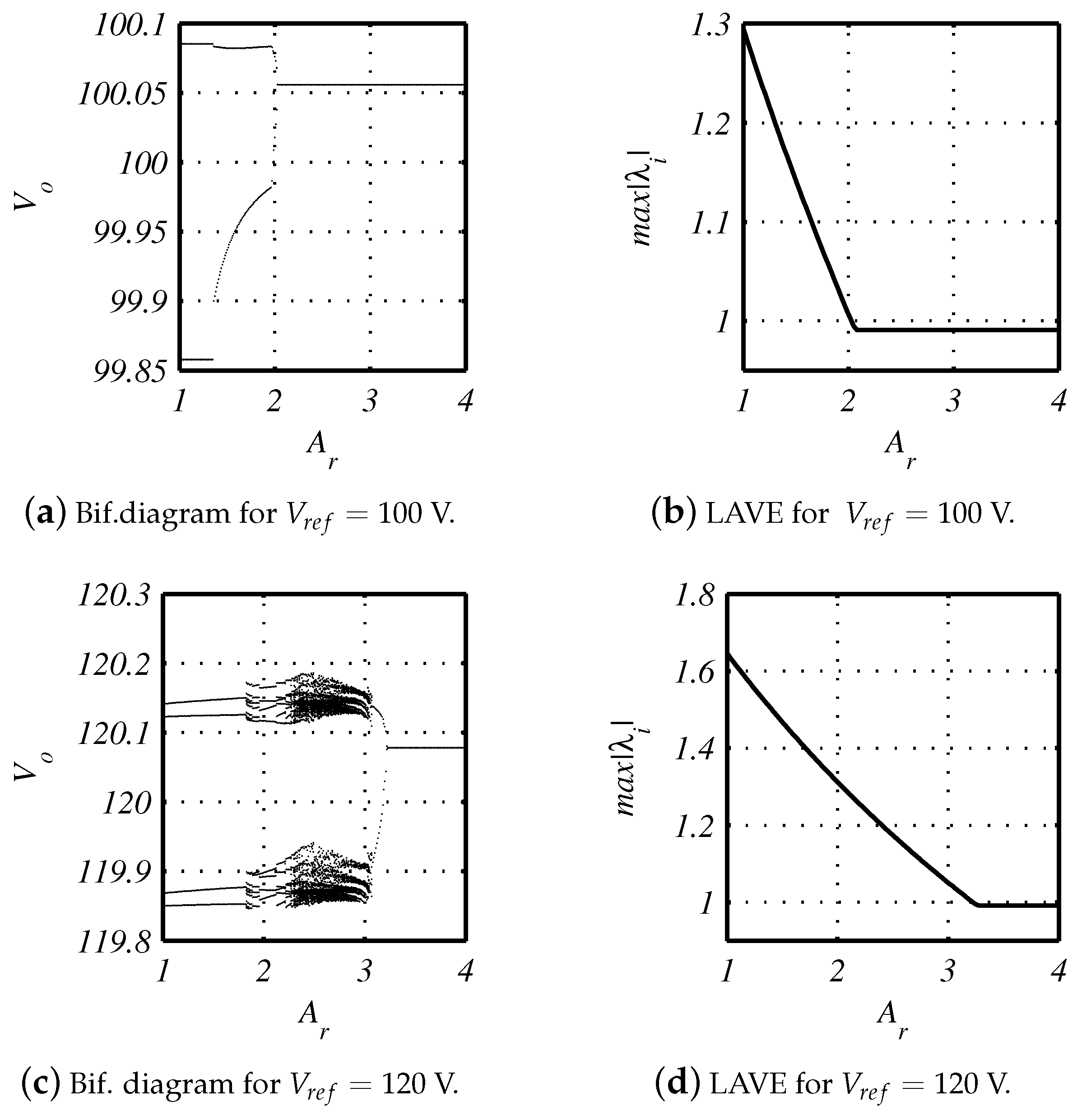
Figure 4a shows results obtained from the proposed approach (see (28)) and V. Figure 4b presents the exact computation using the saltation matrix. Values of exceeding the stability limit guarantee the stability of a Period-1 orbit. In addition, for V, the limit value of the compensation ramp is close to A, and for V, it is close to A (see Figure 4). Figure 4c compares the analytical approach proposed in this paper with the exact value obtained from the saltation matrix; the result is expressed as a percentage. As is shown, the lower the reference voltage, the higher the error value is. In fact, for gain factors greater than six, the approach generates better results. This is due to the assumptions in (7): as the gain factor decreases, the gains of boost and flyback parts cannot be separated. Even more, for gains close to two, only the boost converter works, and the flyback part is voided.
To verify these results, we consider a more complete model of the converter that uses internal resistances of the primary inductor, secondary inductor and MOSFET, as well as the shunt resistance to measure the current (see Table 2). In Figure 5a,c, bifurcation diagrams varying the slope of the ramp are computed while the desired output voltage remains fixed (see Figure 5a for V and Figure 5c for V). In Figure 5b,d, the behavior of the largest absolute value of eigenvalues (LAVE) is shown for the same reference voltage values. In these cases, limit values of the compensation ramp are A and A. These results complement those computed from Equation (27) and Figure 4. Slight displacement is observed between numerical values obtained from equations and from the LAVE due to the assumptions applied.
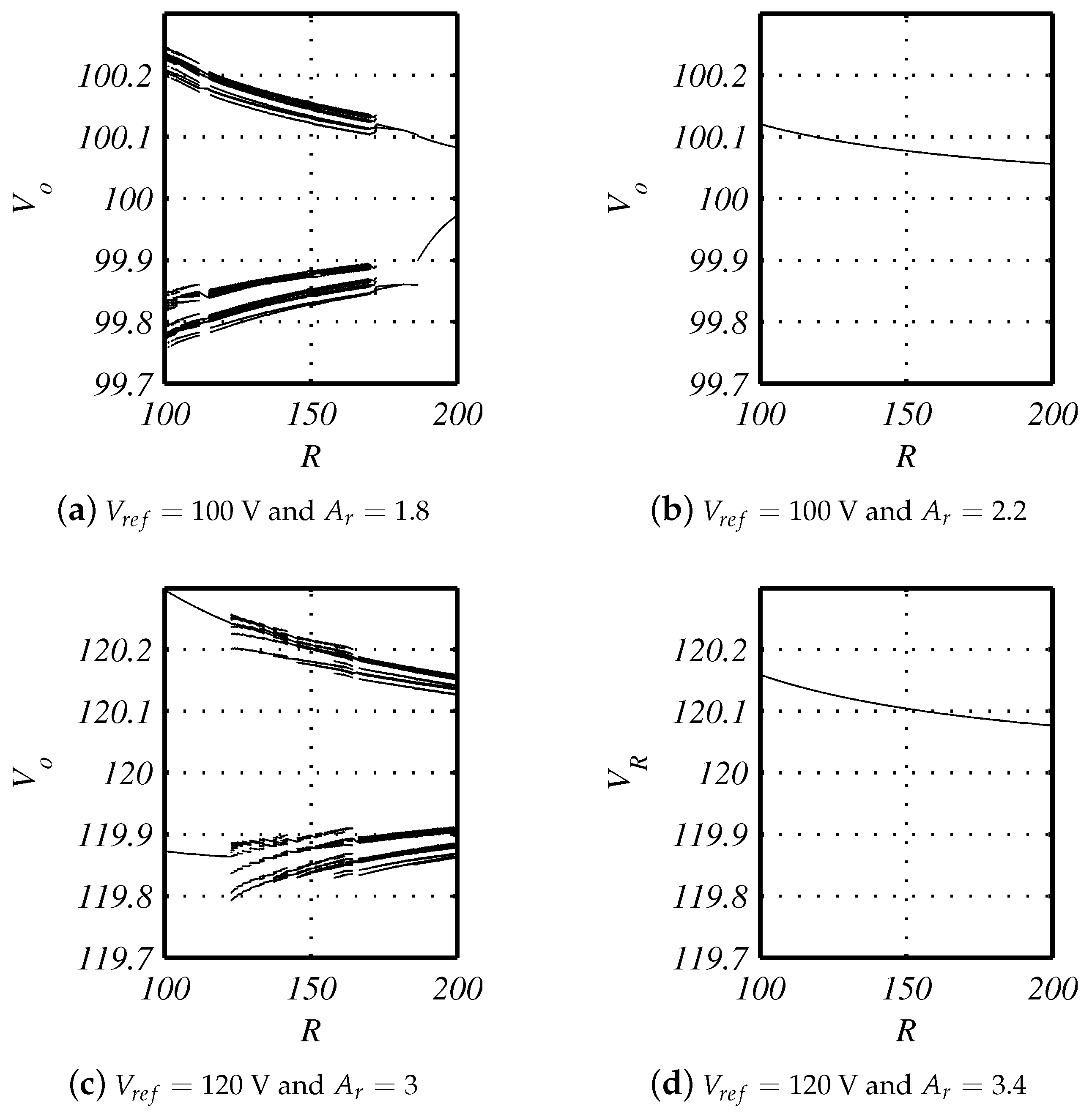
Using the previous limit values, we can find the ramp slopes to stabilize the Period-1 orbit. To prove the robustness of the controller and to compare the system’s behaviors for two values of , changes in the load are induced first by applying V and A. When the load is changed, it can be observed that for the full range of load resistance values, the Period-1 orbit is unstable (see Figure 6a). However, when we fix the slope of the ramp at A (the limit of stability is close to two), the Period-1 orbit is stable for the full range of load resistance values (see Figure 6b). In the second case, we establish V and A. When the load is changed, it can be observed that for the full range of load resistance values, the Period-1 orbit is unstable (see Figure 6c). However, when we fix the slope of the ramp at A (the limit of stability is close to 3.2), the Period-1 orbit is stable for the full load range, as is shown in Figure 6d.
4.2. Experimental Results
To validate the numerical results, an experimental lab prototype that can deliver 100 watts to the load was designed and implemented.The complete design of the circuit is shown in Figure 7. A ferrite core type E is used to design coupled inductors, and the number of turns is calculated using the approach proposed in [57]. Values of the different circuit elements are given in Table 2. The current in the primary coil is measured with non-inductive shunt-resistance (LTO050FR0100FTE3) and then with an instrumentation amplifier ; the output voltage is measured through a voltage divider consisting of and . The signal generated from the voltage divider feeds amplifier . The MOSFET is an with low internal resistance. Finally, two ultrafast diodes ( and ) are used.
The controller is applied using operational amplifiers (). The compensation ramp and clock signals are generated using an (). The amplitude of the compensation ramp is adjusted with a span resistor , and compensates for the offset. Constants and are associated with the PI controller and are obtained from , , and . The measured signals are scaled to from voltage gains ( and ). Constant is given by voltage divider .
Four experiments employed to validate the results shown in the previous section were carried out. All figures of the experimental results show reference current , primary coil current , secondary coil current and output voltage . Therefore, the output voltage and current in the secondary coil are scaled by a factor of 10. The reference current and the current in the primary coil are scaled by a factor of , as mentioned above.
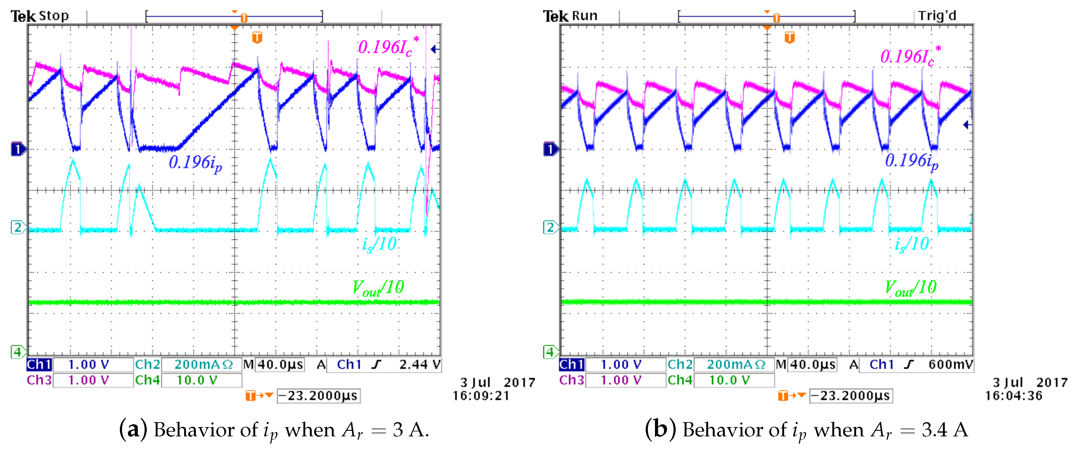
For V (the load resistance is fixed at ; see Table 2), two values of slope compensation are tuned: A and A. When A, the limit set is a Period-2 orbit, as is shown in Figure 8a, but when the ramp compensation increases to A, it converts to a Period-1 orbit (Figure 8b).
For the second experiment, V. In a similar way, two values of slope compensation are tuned: A and A. The behaviors of , , and are shown in Figure 9a,b. For A, a high-period orbit appears, and for A, the Period-1 orbit is stable. These results complement information provided by Equation (28), and the formula can be used to tune the slope of the compensation ramp.
5. Conclusions
This paper enhances the knowledge of the controller design for a boost-flyback converter, which is currently a topic of study.
To achieve high gains with a stable Period-1 orbit when a boost-flyback converter is used, it is necessary to add a compensation ramp to the design. In this work, an analytical expression for computing the value of the compensation ramp slope is presented and mathematically proven. For gains of greater than six, the approach given in this paper has an error of less than .
In general, the results of the equation derived from our computations agree with those of experiments, with minor discrepancies in exact solutions observed for gains of less than six, mainly because certain assumptions are too strong to apply to the real system, and these are not included in the model for the sake of simplicity. This difference is negligible for high step-up gains, for which our approach offers the major benefit of using a formula that guarantees stability while preventing overcompensation and the use of very complex computations.
Author Contributions
Conceptualization, F.A. Formal analysis, J.-G.M. and F.A. Funding acquisition, F.A. and G.O. Investigation, J.-G.M. Project administration, F.A. Software, J.-G.M., G.G. and G.O. Supervision, F.A. and G.O. Validation, J.-G.M. Writing, original draft, J.-G.M. and G.G. Writing, review and editing, F.A. and G.O.
Funding
This work was supported by Universidad Nacional de Colombia, Manizales, Project 31492 from Vicerrectoría de Investigación, DIMA, and COLCIENCIASunder Contract FP44842-052-2016 and program Doctorados Nacionales 6172-2013.
Acknowledgments
The authors would like to thank Ángel Cid Pastor and Abdelali el Aroudi from GAEIResearch Center, Universitat Rovira i Virgili, Spain, for their assistance in obtaining experimental results.
Conflicts of Interest
The authors declare no conflict of interest. The founding sponsors had no role in the design of the study; in the collection, analyses or interpretation of data; in the writing of the manuscript; nor in the decision to publish the results.
Appendix A
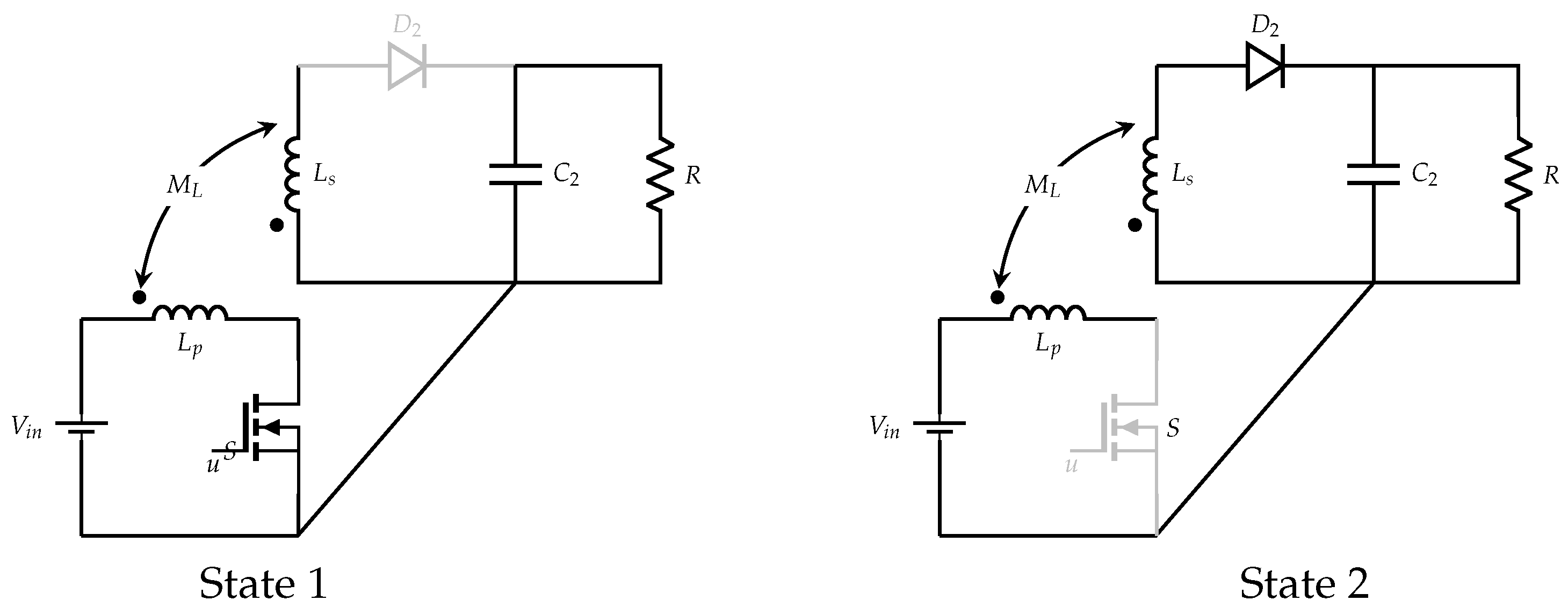
In this Appendix, the procedure to find the ratio between input and output voltages for a flyback converter when coupling factor is different from zero is presented:
The flyback converter operates in two topologies named State 1 and State 2, which are depicted in Figure A1. Voltage equations in primary and secondary coils are given in the general form as:
Figure A1.
Flyback converter topologies.

Depending on the state, voltages and currents can be approximated as:
State 1:
State 2:
such that the average values can be calculated as:
Taking into account , i.e., , we have:
to finally find
Doing , it is easy to prove that this ratio is the same as that reported for a non-magnetically coupled flyback converter.
References
- Acary, V.; Bonnefon, O.; Brogliato, B. Nonsmooth Modeling and Simulation for Switched Circuits; Springer: Berlin, Gremany, 2011. [Google Scholar]
- Banerjee, S.; Verghese, G. Nonlinear Phenomena in Power Electronics: Bifurcations, Chaos, Control, and Applications; Wiley-IEEE Press: Hoboken, NJ, USA, 2001. [Google Scholar]
- Di Bernardo, M.; Budd, C.; Champneys, A.; Kowalczyk, P. Piecewise-Smooth Dynamical Systems, Theory and Applications; Springer: Berlin, Gremany, 2008. [Google Scholar]
- Zhang, X.; Bao, B.; Bao, H.; Wu, Z.; Hu, Y. Bi-Stability Phenomenon in Constant On-Time Controlled Buck Converter with Small Output Capacitor ESR. IEEE Access 2018, 6, 46227–46232. [Google Scholar] [CrossRef]
- Bandyopadhyay, A.; Parui, S. Bifurcation behavior of photovoltaic panel fed Cuk converter connected to different types of loads. In Proceedings of the 2018 International Symposium on Devices, Circuits and Systems (ISDCS), Howrah, India, 29–31 March 2018; pp. 1–5. [Google Scholar] [CrossRef]
- Zhang, R.; Hu, M.; Zhang, Y.; Ma, W.; Zhao, J. Control of bifurcation in the buck converter using novel resonant parametric perturbation. In Proceedings of the IECON 2017—43rd Annual Conference of the IEEE Industrial Electronics Society, Beijing, China, 29 October–1 November 2017; pp. 982–986. [Google Scholar] [CrossRef]
- Samanta, B.; Ghosh, S.; Panda, G.K.; Saha, P.K. Chaos control on current-mode controlled DC-DC boost converter using TDFC. In Proceedings of the 2017 IEEE Calcutta Conference (CALCON), Kolkata, India, 2–3 December 2017; pp. 159–163. [Google Scholar] [CrossRef]
- Deane, J.H.B.; Hamill, D.C. Chaotic behaviour in current-mode controlled DC-DC convertor. Electron. Lett. 1991, 27, 1172–1173. [Google Scholar] [CrossRef]
- di Bernardo, M.; Garefalo, F.; Glielmo, L.; Vasca, F. Analysis of chaotic buck, boost and buck-boost converters through switching maps. In Proceedings of the PESC97, Record 28th Annual IEEE Power Electronics Specialists Conference. Formerly Power Conditioning Specialists Conference 1970–71. Power Processing and Electronic Specialists Conference 1972, Saint Louis, MO, USA, 27 June 1997; Volume 1, pp. 754–760. [Google Scholar] [CrossRef]
- Aroudi, A.E.; Mandal, K.; Giaouris, D.; Banerjee, S. Self-compensation of DC–DC converters under peak current mode control. Electron. Lett. 2017, 53, 345–347. [Google Scholar] [CrossRef]
- Fossas, E.; Olivar, G. Study of chaos in the buck converter. IEEE Trans. Circuits Syst. I Fundam. Theory Appl. 1996, 43, 13–25. [Google Scholar] [CrossRef] [Green Version]
- Zhusubaliyev, Z.T.; Mosekilde, E. Torus birth bifurcations in a DC/DC converter. IEEE Trans. Circuits Syst. I Regul. Pap. 2006, 53, 1839–1850. [Google Scholar] [CrossRef]
- Leine, R.I.; Nijmeijer, H. Dynamics and Bifurcations of Non-Smooth Mechanical Systems; Springer: Berlin, Germnay, 2004. [Google Scholar]
- Wu, H.; Pickert, V.; Deng, X.; Giaouris, D.; Li, W.; He, X. Polynomial Curve Slope Compensation for Peak-Current-Mode-Controlled Power Converters. IEEE Trans. Ind. Electron. 2019, 66, 470–481. [Google Scholar] [CrossRef]
- Wu, Y.E.; Chiu, P.N. A High-Efficiency Isolated-Type Three-Port Bidirectional DC/DC Converter for Photovoltaic Systems. Energies 2017, 10, 434. [Google Scholar] [CrossRef]
- Choudhury, T.R.; Dhara, S.; Nayak, B.; Santra, S.B. Modelling of a high step up DC-DC converter based on Boost-flyback-switched capacitor. In Proceedings of the 2017 IEEE Calcutta Conference (CALCON), Kolkata, India, 2–3 December 2017; pp. 248–252. [Google Scholar] [CrossRef]
- Shen, C.L.; Chiu, P.C. Buck-boost-flyback integrated converter with single switch to achieve high voltage gain for PV or fuel-cell applications. IET Power Electron. 2016, 9, 1228–1237. [Google Scholar] [CrossRef]
- Lodh, T.; Majumder, T. Highly efficient and compact Sepic-Boost-Flyback integrated converter with multiple outputs. In Proceedings of the 2016 International Conference on Signal Processing, Communication, Power and Embedded System (SCOPES), Paralakhemundi, India, 3–5 October 2016; pp. 6–11. [Google Scholar] [CrossRef]
- Arango, E.; Ramos-Paja, C.A.; Calvente, J.; Giral, R.; Serna, S. Asymmetrical Interleaved DC/DC Switching Converters for Photovoltaic and Fuel Cell Applications-Part 1: Circuit Generation, Analysis and Design. Energies 2012, 5, 4590–4623. [Google Scholar] [CrossRef]
- Liu, H.; Hu, H.; Wu, H.; Xing, Y.; Batarseh, I. Overview of High-Step-Up Coupled-Inductor Boost Converters. IEEE J. Emerg. Sel. Top. Power Electron. 2016, 4, 689–704. [Google Scholar] [CrossRef]
- Wang, Y.F.; Yang, L.; Wang, C.S.; Li, W.; Qie, W.; Tu, S.J. High Step-Up 3-Phase Rectifier with Fly-Back Cells and Switched Capacitors for Small-Scaled Wind Generation Systems. Energies 2015, 8, 2742–2768. [Google Scholar] [CrossRef] [Green Version]
- Zhao, Q.; Lee, F.C. High performance coupled-inductor DC-DC converters. In Proceedings of the Eighteenth Annual IEEE Applied Power Electronics Conference and Exposition (APEC ’03), Miami Beach, FL, USA, 9–13 February 2003; Volume 1, pp. 109–113. [Google Scholar]
- Tseng, K.; Liang, T. Novel high-efficiency step-up converter. IEE Proc. Electr. Power Appl. 2004, 151, 182–190. [Google Scholar] [CrossRef]
- Lai, C.M.; Yang, M.J. A High-Gain Three-Port Power Converter with Fuel Cell, Battery Sources and Stacked Output for Hybrid Electric Vehicles and DC-Microgrids. Energies 2016, 9, 180. [Google Scholar] [CrossRef]
- Tseng, K.C.; Lin, J.T.; Cheng, C.A. An Integrated Derived Boost-Flyback Converter for fuel cell hybrid electric vehicles. In Proceedings of the 2013 1st International Future Energy Electronics Conference (IFEEC), Tainan, Taiwan, 3–6 November 2013; pp. 283–287. [Google Scholar]
- Park, J.H.; Kim, K.T. Multi-output differential power processing system using boost-flyback converter for voltage balancing. In Proceedings of the 2017 International Conference on Recent Advances in Signal Processing, Telecommunications Computing (SigTelCom), Da Nang, Vietnam, 9–11 January 2017; pp. 139–142. [Google Scholar] [CrossRef]
- Chen, S.M.; Wang, C.Y.; Liang, T.J. A novel sinusoidal boost-flyback CCM/DCM DC-DC converter. In Proceedings of the 2014 IEEE Applied Power Electronics Conference and Exposition—APEC 2014, Fort Worth, TX, USA, 16–20 March 2014; pp. 3512–3516. [Google Scholar]
- Lee, S.W.; Do, H.L. A Single-Switch AC-DC LED Driver Based on a Boost-Flyback PFC Converter with Lossless Snubber. IEEE Trans. Power Electron. 2017, 32, 1375–1384. [Google Scholar] [CrossRef]
- Divya, K.M.; Parackal, R. High power factor integrated buck-boost flyback converter driving multiple outputs. In Proceedings of the 2015 Online International Conference on Green Engineering and Technologies (IC-GET), Coimbatore, India, 27 November 2015; pp. 1–5. [Google Scholar] [CrossRef]
- Xu, D.; Cai, Y.; Chen, Z.; Zhong, S. A novel two winding coupled-inductor step-up voltage gain boost-flyback converter. In Proceedings of the 2014 International Power Electronics and Application Conference and Exposition, Shanghai, China, 5–8 November 2014; pp. 1–5. [Google Scholar]
- Zhang, J.; Wu, H.; Xing, Y.; Sun, K.; Ma, X. A variable frequency soft switching boost-flyback converter for high step-up applications. In Proceedings of the 2011 IEEE Energy Conversion Congress and Exposition, Phoenix, AZ, USA, 17–22 September 2011; pp. 3968–3973. [Google Scholar]
- Ding, X.; Yu, D.; Song, Y.; Xue, B. Integrated switched coupled-inductor boost-flyback converter. In Proceedings of the 2017 IEEE Energy Conversion Congress and Exposition (ECCE), Cincinnati, OH, USA, 1–5 October 2017; pp. 211–216. [Google Scholar] [CrossRef]
- Erickson, R.W.; Maksimovic, D. Fundamentals of Power Electronics; Springer: Berlin, Germnay, 2001. [Google Scholar]
- Wang, Y.; Xu, J.; Zhou, S.; Zhao, T.; Liao, K. Current-mode controlled single-inductor dual-output buck converter with ramp compensation. In Proceedings of the 2017 IEEE Energy Conversion Congress and Exposition (ECCE), Cincinnati, OH, USA, 1–5 October 2017; pp. 4996–5000. [Google Scholar] [CrossRef]
- Abdelhamid, E.; Bonanno, G.; Corradini, L.; Mattavelli, P.; Agostinelli, M. Stability Properties of the 3-Level Flying Capacitor Buck Converter Under Peak or Valley Current-Programmed-Control. In Proceedings of the 2018 IEEE 19th Workshop on Control and Modeling for Power Electronics (COMPEL), Padua, Italy, 25–28 June 2018; pp. 1–8. [Google Scholar] [CrossRef]
- Zhou, S.; Zhou, G.; Zeng, S.; Zhao, H.; Xu, S. Unified modelling and dynamical analysis of current-mode controlled single-inductor dual-output switching converter with ramp compensation. IET Power Electron. 2018, 11, 1297–1305. [Google Scholar] [CrossRef]
- Ridley, R.B. A new continuous-time model for current-mode control with constant frequency, constant on-time, and constant off-time, in CCM and DCM. In Proceedings of the 21st Annual IEEE Conference on Power Electronics Specialists, San Antonio, TX, USA, 11–14 June 1990; pp. 382–389. [Google Scholar] [CrossRef]
- Unitrode-Corporation. Modeling, Analysis and Compensation of the Current-Mode Converter. 1999. Available online: http://www.ti.com/general/docs/litabsmultiplefilelist.tsp?literatureNumber=slua101 (accessed on 7 October 2018).
- Yang, Y.Z.; Xie, G.J. Research and design of a self-adaptable slope compensation circuit with simple structure. In Proceedings of the 2010 IEEE International Conference on Intelligent Computing and Intelligent Systems, Xiamen, China, 29–31 October 2010; Volume 2, pp. 333–335. [Google Scholar] [CrossRef]
- Yang, C.; Wang, C.; Kuo, T. Current-Mode Converters with Adjustable-Slope Compensating Ramp. In Proceedings of the APCCAS 2006—2006 IEEE Asia Pacific Conference on Circuits and Systems, Singapore, 4–7 December 2006; pp. 654–657. [Google Scholar] [CrossRef]
- Jiuming, Z.; Shulin, L. Design of slope compensation circuit in peak-current controlled mode converters. In Proceedings of the 2011 International Conference on Electric Information and Control Engineering (ICEICE), Wuhan, China, 15–17 April 2011; pp. 1310–1313. [Google Scholar]
- Grote, T.; Schafmeister, F.; Figge, H.; Frohleke, N.; Ide, P.; Bocker, J. Adaptive digital slope compensation for peak current mode control. In Proceedings of the Energy Conversion Congress and Exposition (ECCE 2009), San Jose, CA, USA, 20–24 September 2009; pp. 3523–3529. [Google Scholar]
- Chen, Y.; Tse, C.K.; Wong, S.C.; Qiu, S.S. Interaction of fast-scale and slow-scale bifurcations in current-mode controlled DC/DC converters. Int. J. Bifurc. Chaos 2007, 17, 1609–1622. [Google Scholar] [CrossRef]
- Chen, Y.; Tse, C.K.; Qiu, S.S.; Lindenmuller, L.; Schwarz, W. Coexisting Fast-Scale and Slow-Scale Instability in Current-Mode Controlled DC/DC Converters: Analysis, Simulation and Experimental Results. IEEE Trans. Circuits Syst. I Regul. Pap. 2008, 55, 3335–3348. [Google Scholar] [CrossRef] [Green Version]
- El Aroudi, A. A New Approach for Accurate Prediction of Subharmonic Oscillation in Switching Regulators Part I: Mathematical Derivations. IEEE Trans. Power Electron. 2017, 32, 5651–5665. [Google Scholar] [CrossRef]
- El Aroudi, A. A New Approach for Accurate Prediction of Subharmonic Oscillation in Switching Regulators Part II: Case Studies. IEEE Trans. Power Electron. 2017, 32, 5835–5849. [Google Scholar] [CrossRef]
- Fang, C.C.; Redl, R. Subharmonic Instability Limits for the Peak-Current-Controlled Buck Converter with Closed Voltage Feedback Loop. IEEE Trans. Power Electron. 2015, 30, 1085–1092. [Google Scholar] [CrossRef]
- Fang, C.C.; Redl, R. Subharmonic Instability Limits for the Peak-Current-Controlled Boost, Buck-Boost, Flyback, and SEPIC Converters With Closed Voltage Feedback Loop. IEEE Trans. Power Electron. 2017, 32, 4048–4055. [Google Scholar] [CrossRef]
- Liu, P.; Yan, Y.; Lee, F.C.; Mattavelli, P. Universal Compensation Ramp Auto-Tuning Technique for Current Mode Controls of Switching Converters. IEEE Trans. Power Electron. 2018, 33, 970–974. [Google Scholar] [CrossRef]
- Lu, W.G.; Lang, S.; Li, A.; Iu, H.H.C. Limit-cycle stable control of current-mode dc-dc converter with zero-perturbation dynamical compensation. Int. J. Circuit Theory Appl. 2015, 43, 318–328. [Google Scholar] [CrossRef]
- Munoz, J.G.; Gallo, G.; Osorio, G.; Angulo, F. Performance Analysis of a Peak-Current Mode Control with Compensation Ramp for a Boost-Flyback Power Converter. J. Control Sci. Eng. 2016, 2016, 7354791. [Google Scholar] [CrossRef]
- Muñoz, J.G.; Gallo, G.; Angulo, F.; Osorio, G. Coexistence of solutions in a boost-flyback converter with current mode control. In Proceedings of the 2017 IEEE 8th Latin American Symposium on Circuits Systems (LASCAS), Bariloche, Argentina, 20–23 February 2017; pp. 1–4. [Google Scholar] [CrossRef]
- Liang, T.; Tseng, K. Analysis of integrated boost-flyback step-up converter. IEE Proc. Electr. Power Appl. 2005, 152, 217–225. [Google Scholar] [CrossRef]
- Carrero Candelas, N.A. Modelado, Simulación y Control de un Convertidor Boost Acoplado Magnéticamente. Ph.D. Thesis, Universidad Politécnica de Catalunya, Barcelona, Spain, 2014. [Google Scholar]
- Elbkosh, A.; Giaouris, D.; Pickert, V.; Zahawi, B.; Banerjee, S. Stability analysis and control of bifurcations of parallel connected DC/DC converters using the monodromy matrix. In Proceedings of the IEEE International Symposium on Circuits and Systems (ISCAS 2008), Seattle, WA, USA, 18–21 May 2008; pp. 556–559. [Google Scholar]
- Morcillo Bastidas, J.; Burbano Lombana, D.; Angulo, F. Adaptive Ramp Technique for Controlling Chaos and Sub-harmonic Oscillations in DC-DC Power Converters. IEEE Trans. Power Electron. 2016, 31, 5330–5343. [Google Scholar] [CrossRef]
- Dixon, L. Coupled Inductor Design. 1993. Available online: http://www.ti.com/lit/ml/slup105/slup105.pdf (accessed on 4 August 2018).
Figure 1.
Boost-flyback converter with peak current-mode control.
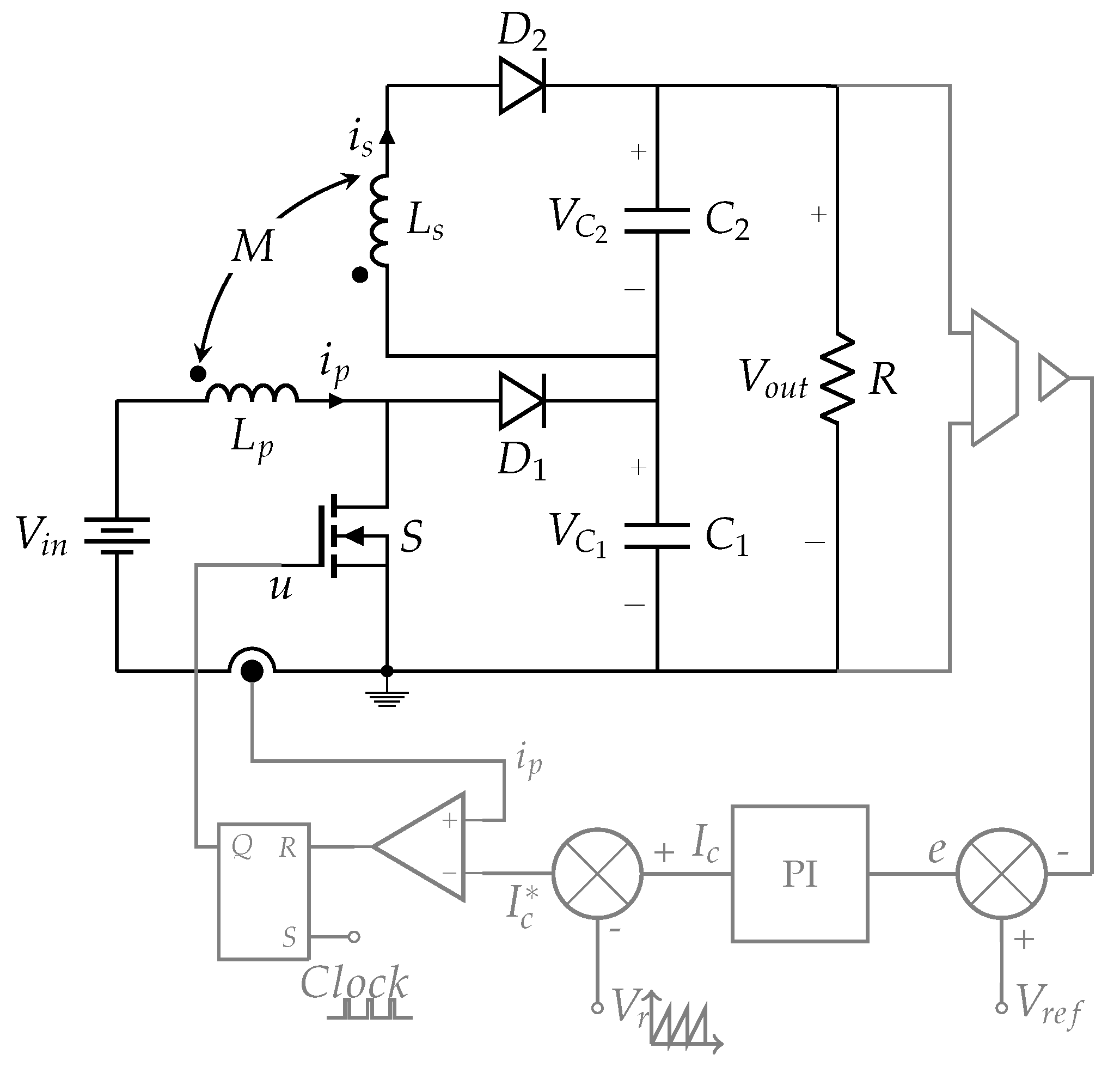
Figure 2.
Typical behavior of the currents flowing by the coils in the steady state of a Period-1 orbit.
Figure 2.
Typical behavior of the currents flowing by the coils in the steady state of a Period-1 orbit.

Figure 3.
Primary- and secondary-coil currents for the Period-1 orbit and a perturbed solution.
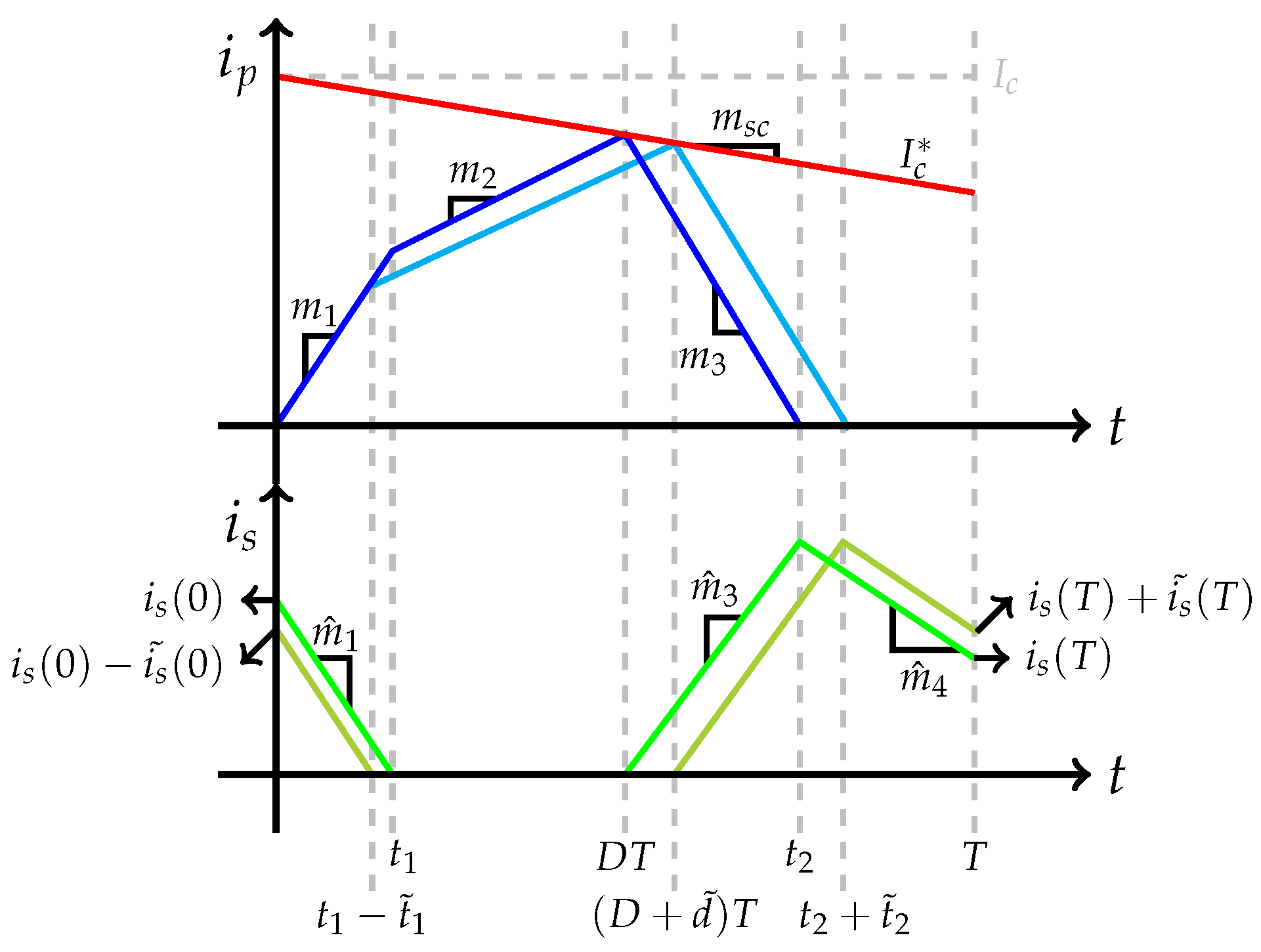
Figure 4.
Value of the slope compensation. (a) Approach proposed in this paper. (b) Exact value obtained with the saltation matrix and (c) percentage error.
Figure 4.
Value of the slope compensation. (a) Approach proposed in this paper. (b) Exact value obtained with the saltation matrix and (c) percentage error.
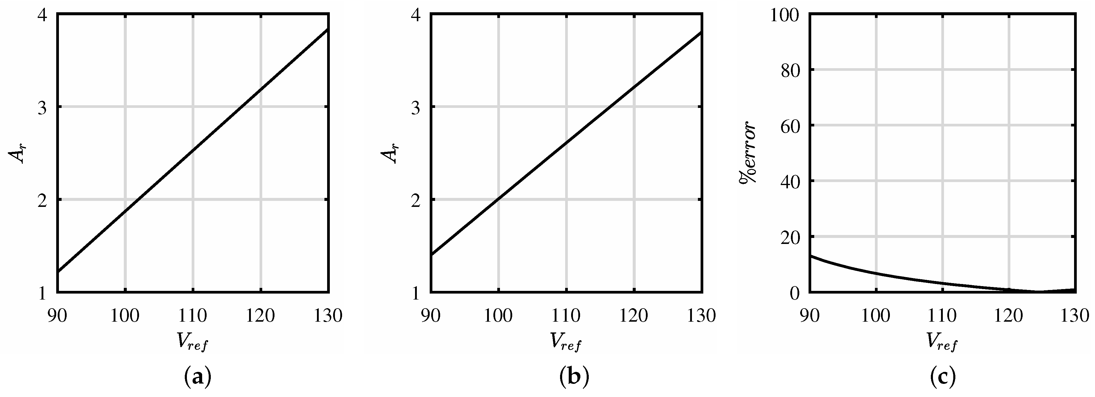
Figure 5.
Bifurcation diagrams and largest absolute value of eigenvalues (LAVE) evolution for variations.
Figure 5.
Bifurcation diagrams and largest absolute value of eigenvalues (LAVE) evolution for variations.

Figure 6.
Bifurcation diagrams varying the load resistance R.

Figure 7.
Experimental circuit.

Figure 8.
Experimental results with two different values of the compensation ramp for V.
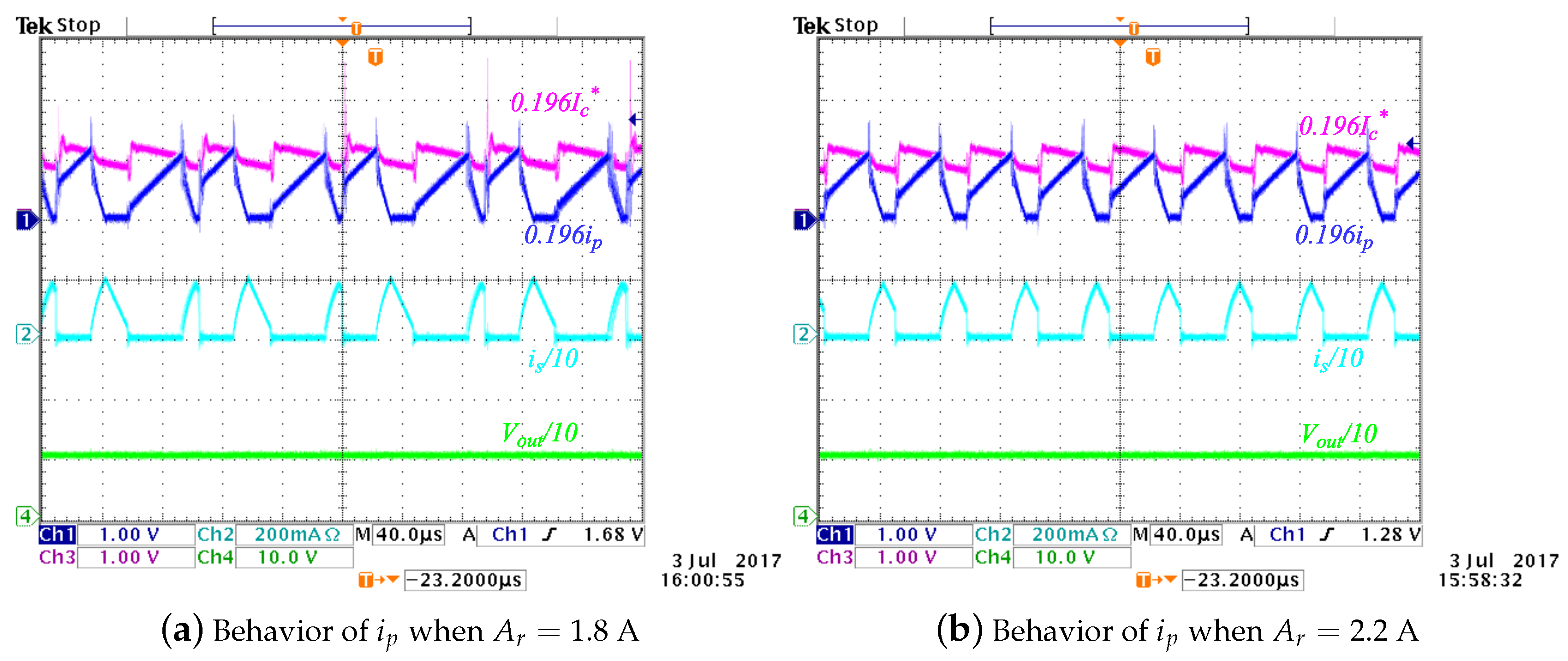
Figure 9.
Experimental results with two different values of the compensation ramp for V.

Table 1.
States of the Period-1 orbit.
| State | S | ||
|---|---|---|---|
| ON | ON | OFF | |
| ON | OFF | OFF | |
| OFF | ON | ON | |
| OFF | ON | OFF |
Table 2.
Converter and experimental setup parameters.
| Converter’s Parameters | Experiment’s Parameters | ||||
|---|---|---|---|---|---|
| Element | Value | Element | Value | Electronic Device | Reference |
| 18 V | 1 M | INA128p | |||
| 129.2 H | 20 k | TL084 | |||
| 484.9 H | 100 k | LM311 | |||
| 0.0268 | k | 555 | |||
| 0.1307 | 10 k | 74XX02 | |||
| k | 0.995 | 200 k | IRF2110 | ||
| 220 F | k | 74XX08 | |||
| 220 F | F | 2N3906 | |||
| R | 200 | 10 nF | D | 1N4148 | |
| 2 A/V | 0.01 | ||||
| 350 A/(V.s) | |||||
| T | 50 s | ||||
© 2018 by the authors. Licensee MDPI, Basel, Switzerland. This article is an open access article distributed under the terms and conditions of the Creative Commons Attribution (CC BY) license (http://creativecommons.org/licenses/by/4.0/).
Share and Cite
MDPI and ACS Style
Muñoz, J.-G.; Gallo, G.; Angulo, F.; Osorio, G. Slope Compensation Design for a Peak Current-Mode Controlled Boost-Flyback Converter. Energies 2018, 11, 3000. https://doi.org/10.3390/en11113000
AMA Style
Muñoz J-G, Gallo G, Angulo F, Osorio G. Slope Compensation Design for a Peak Current-Mode Controlled Boost-Flyback Converter. Energies. 2018; 11(11):3000. https://doi.org/10.3390/en11113000
Chicago/Turabian StyleMuñoz, Juan-Guillermo, Guillermo Gallo, Fabiola Angulo, and Gustavo Osorio. 2018. "Slope Compensation Design for a Peak Current-Mode Controlled Boost-Flyback Converter" Energies 11, no. 11: 3000. https://doi.org/10.3390/en11113000
Note that from the first issue of 2016, this journal uses article numbers instead of page numbers. See further details here.