A Simple Method for Reducing THD and Improving the Efficiency in CSI Topology Based on SiC Power Devices


Abstract
:1. Introduction
2. Power Converters Analysis and Description of the Proposed Method
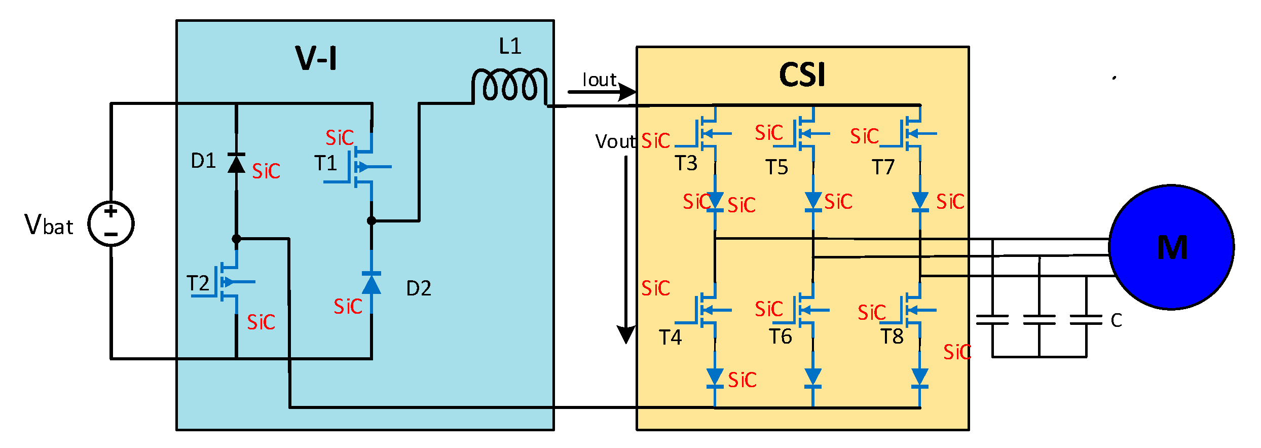
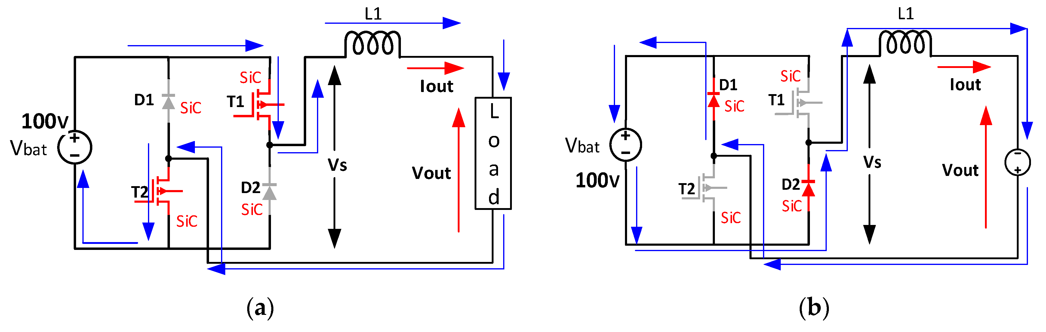
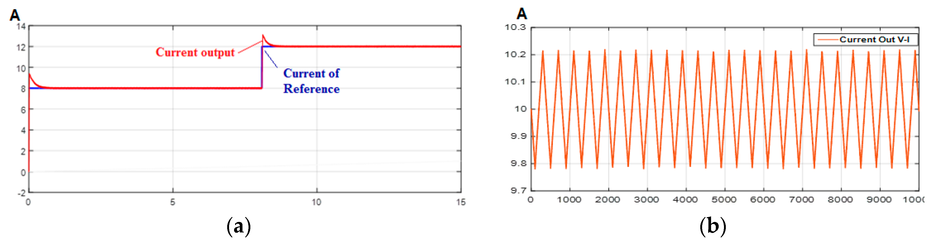
2.1. V-I Converter and CSI Inverter Analysis
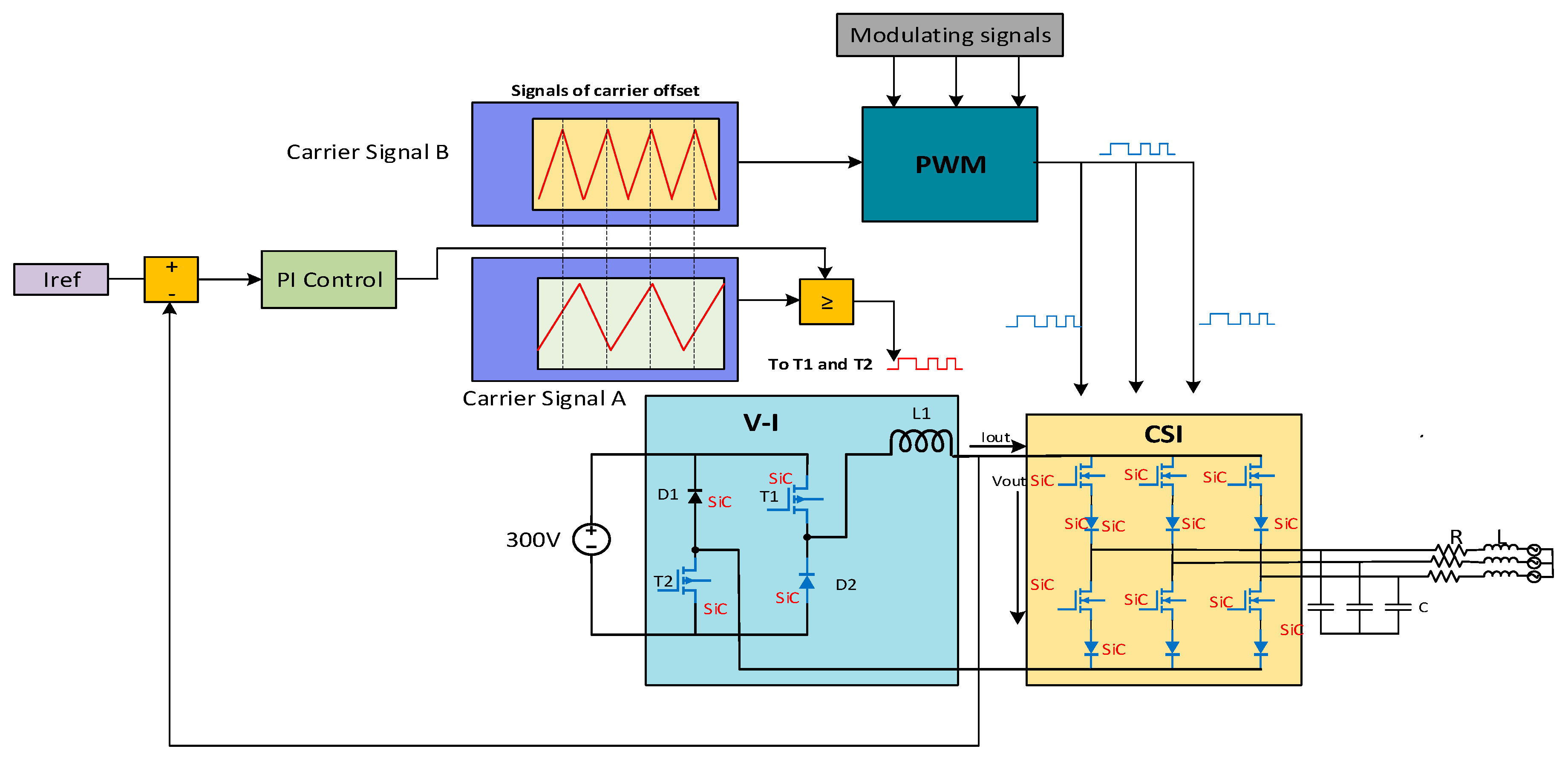
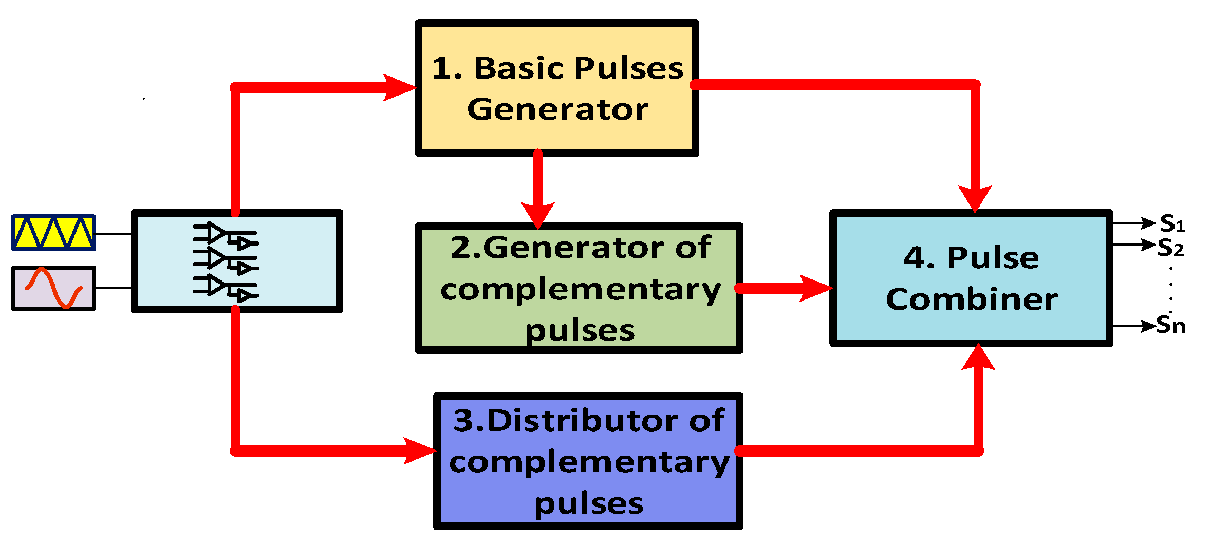
2.2. Proposed Method Description
3. Operation of CSI and Validation
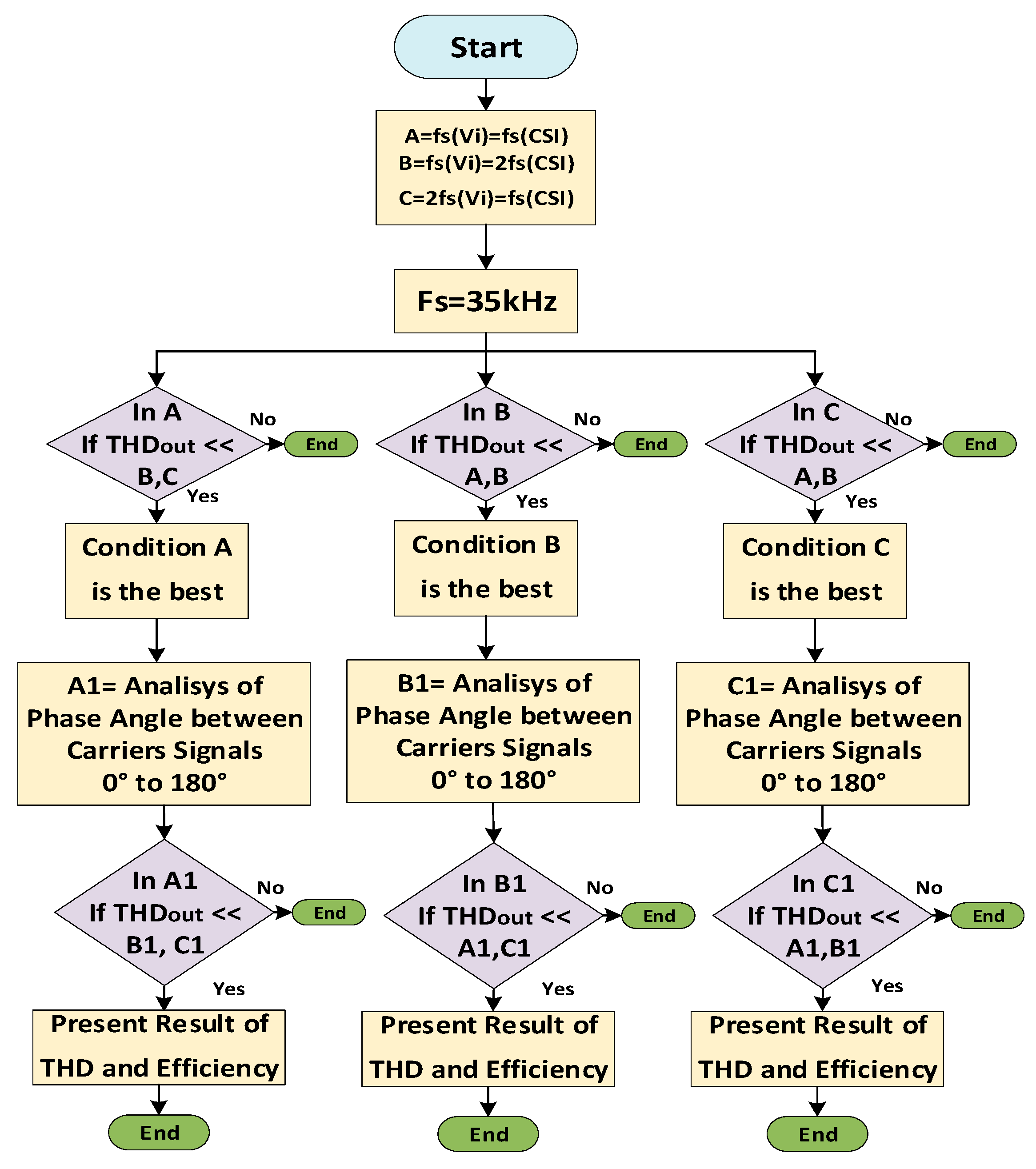
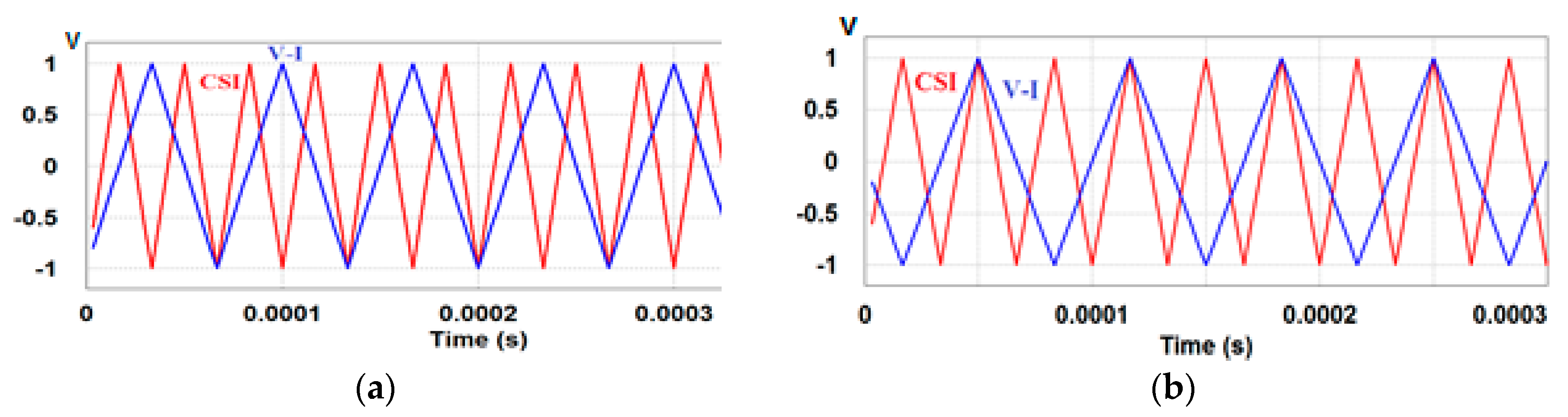
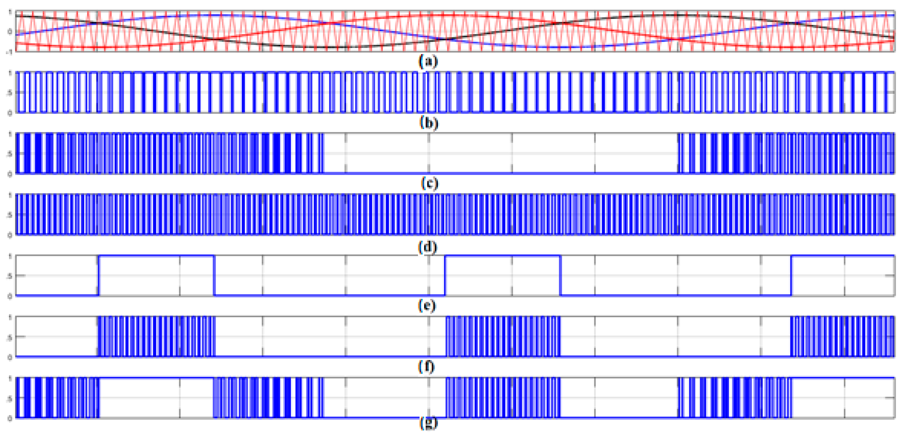
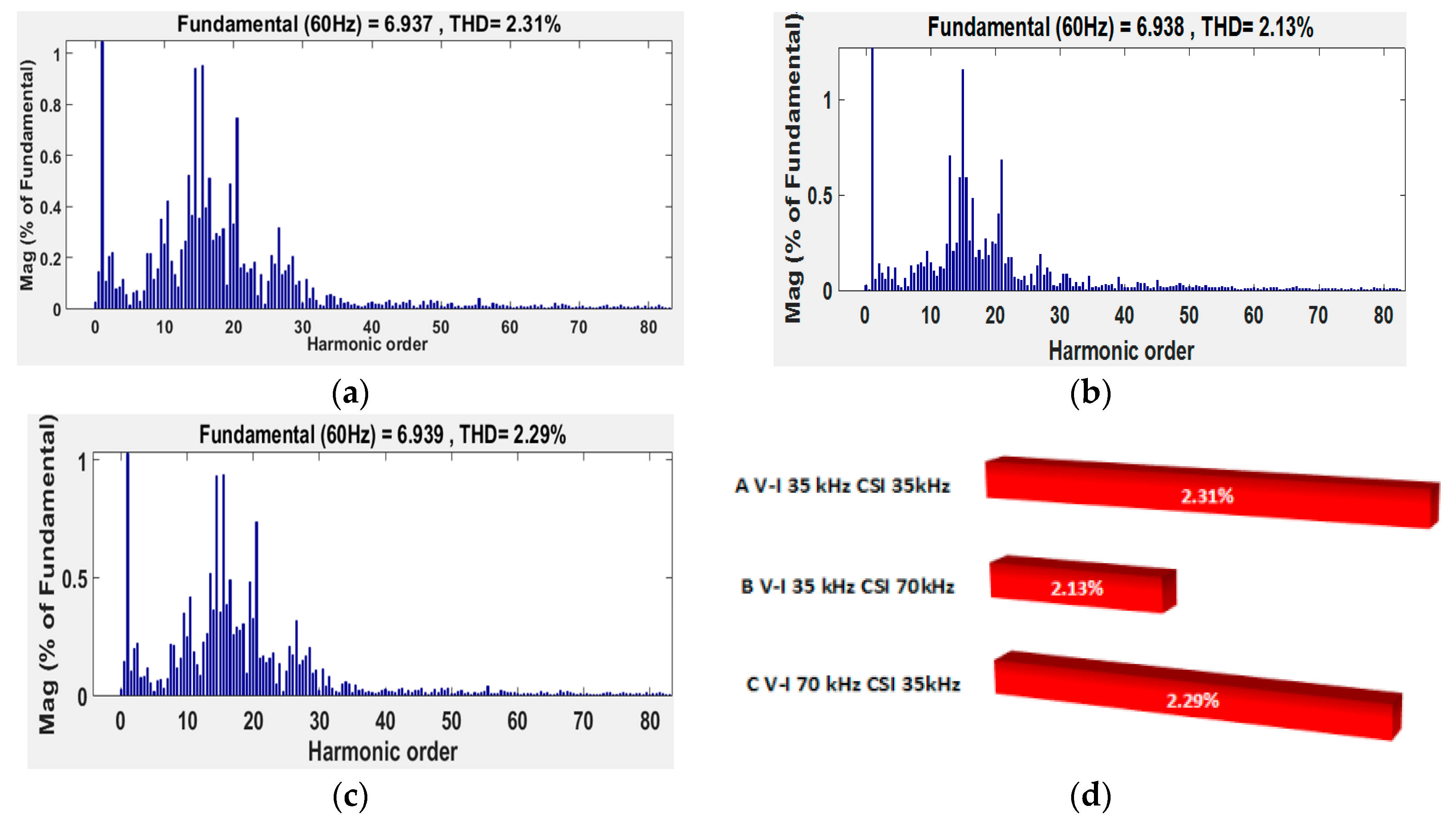
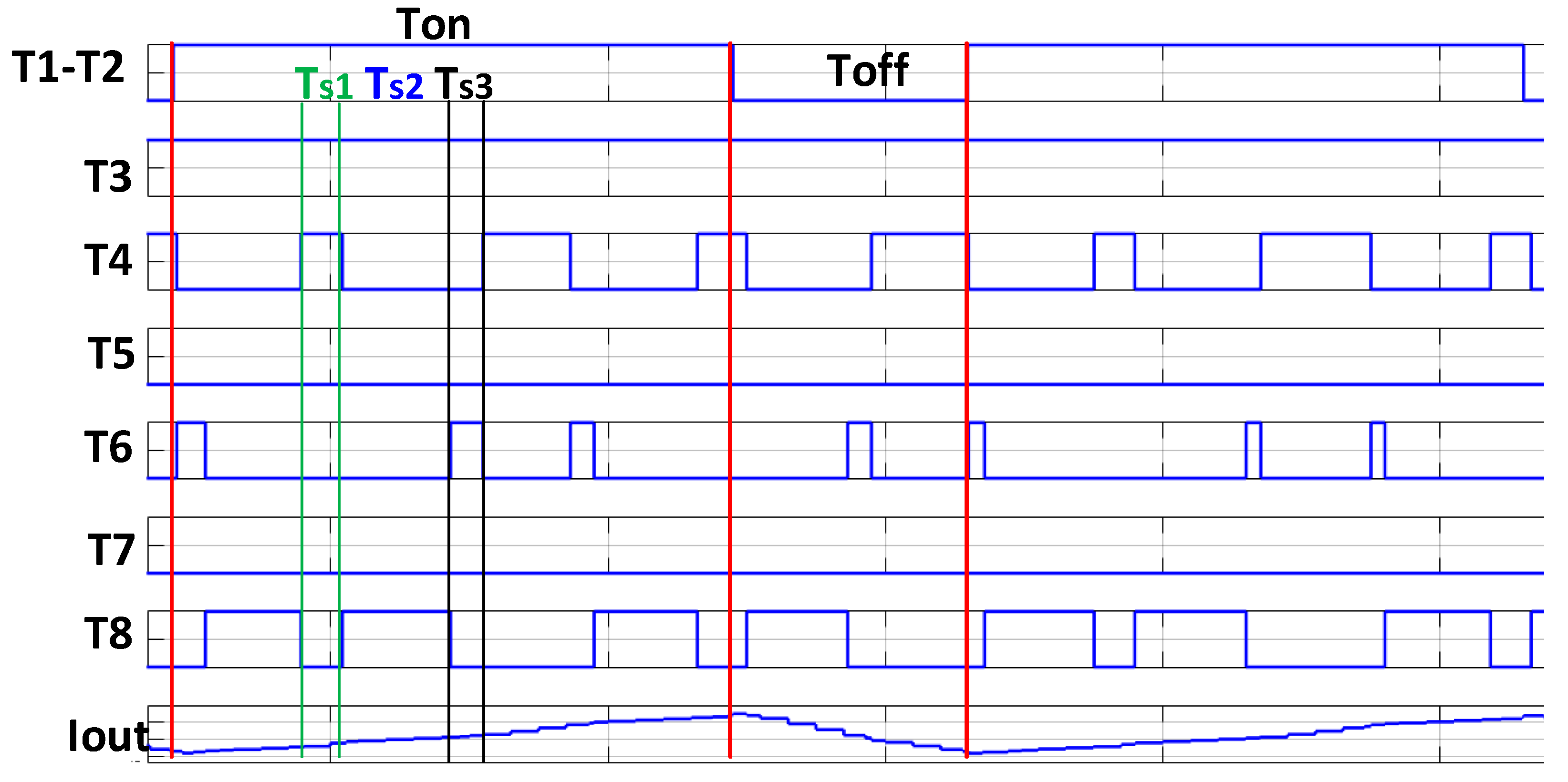
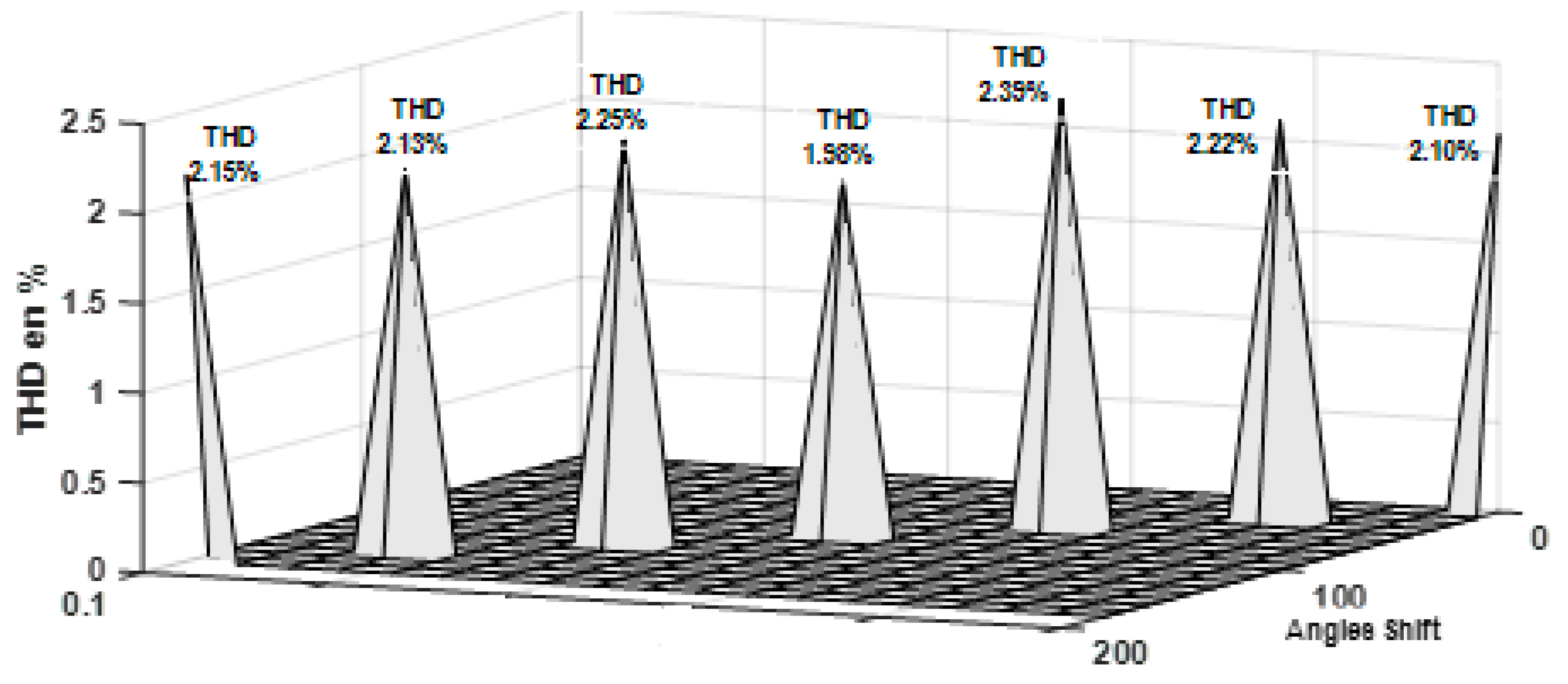
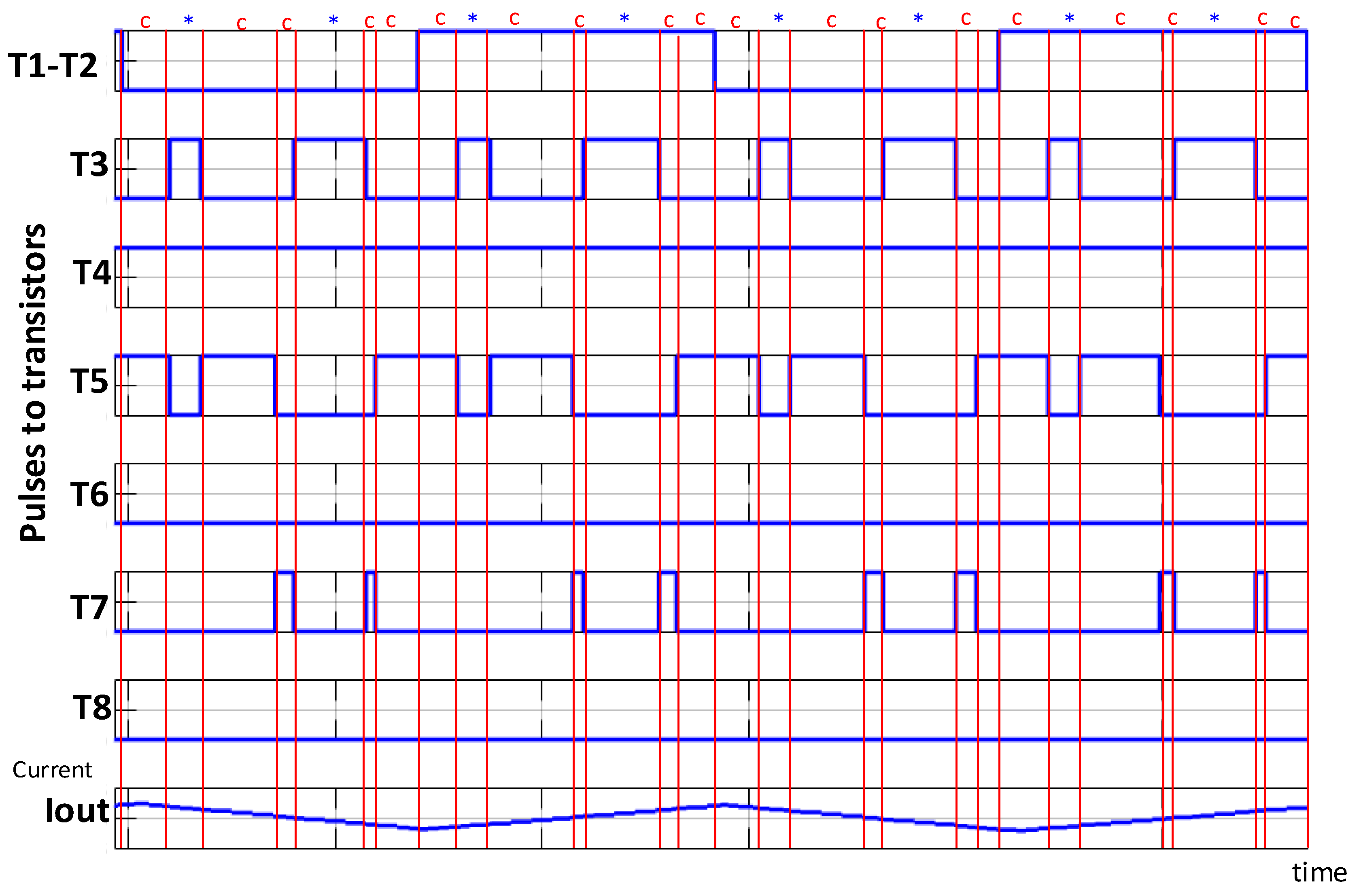
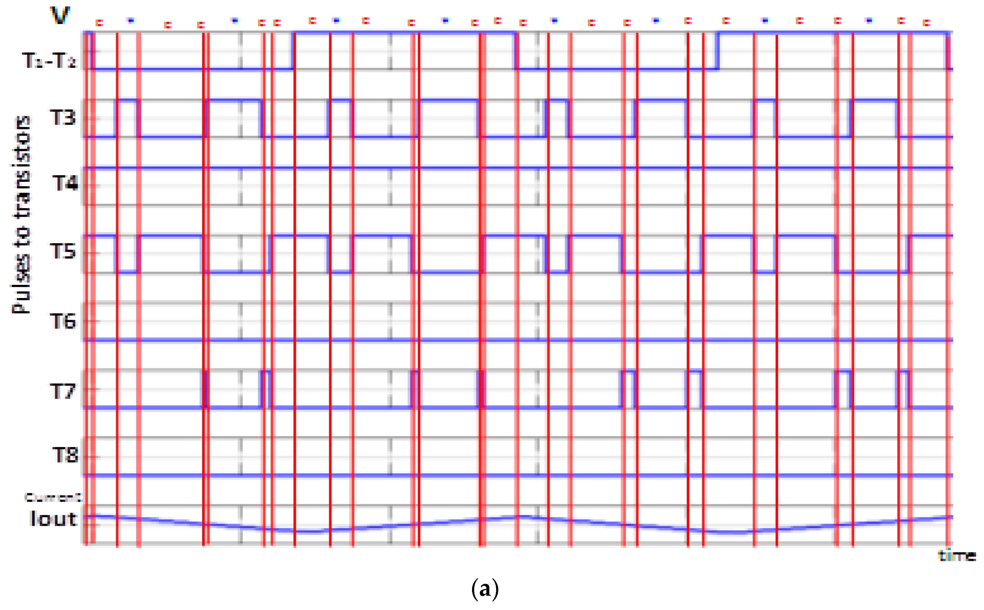
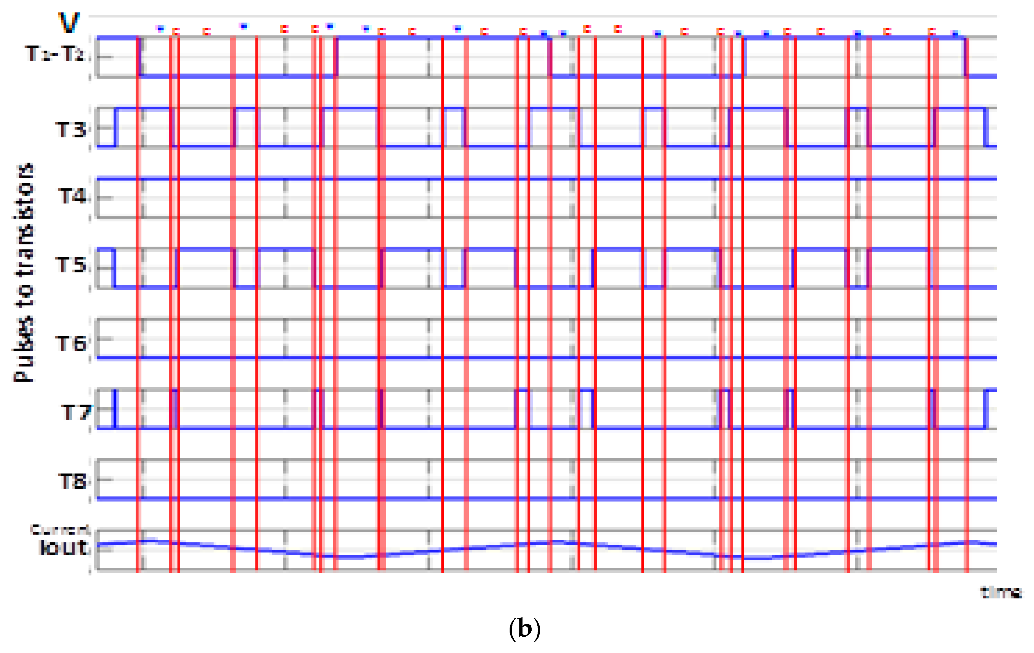
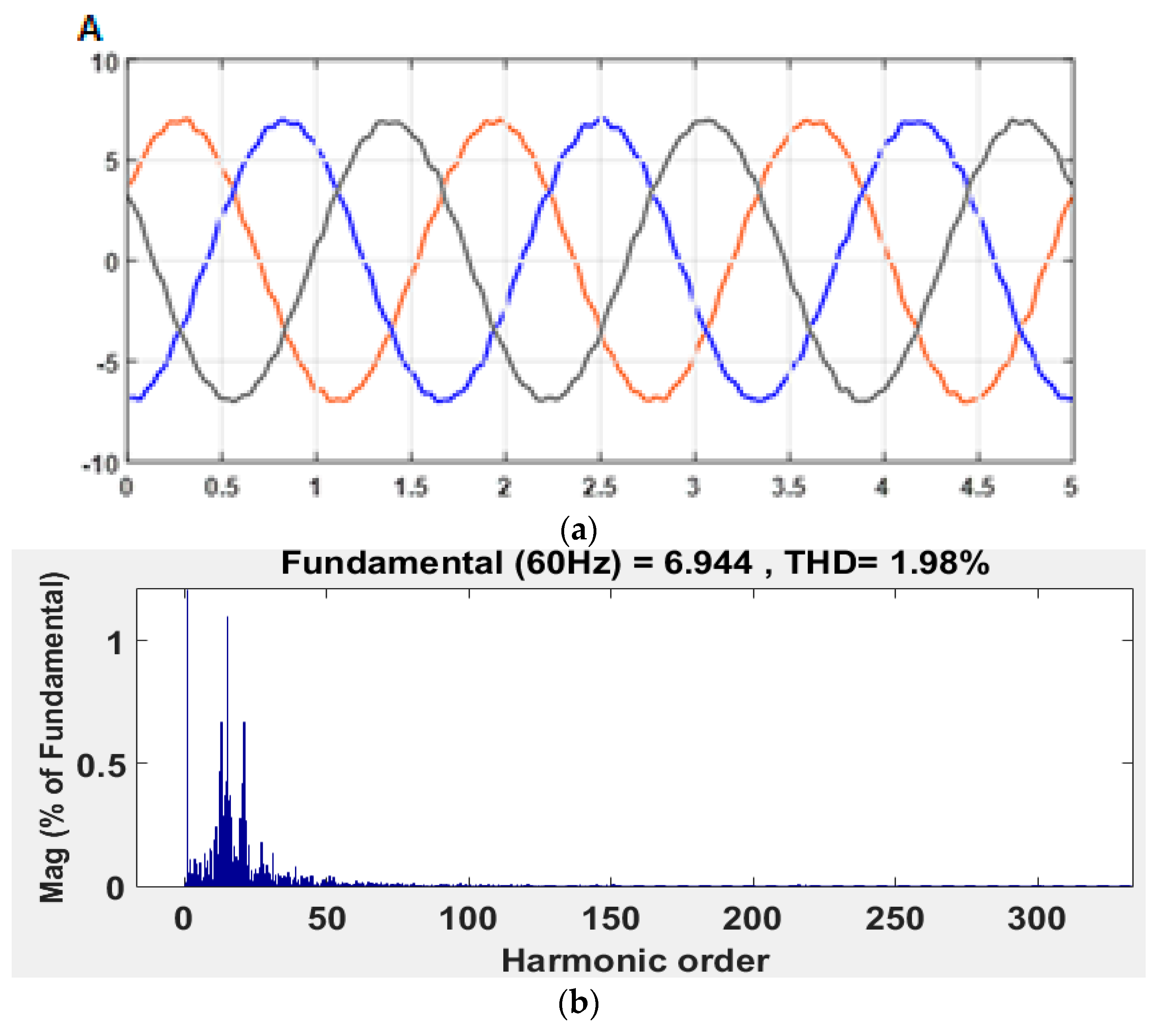
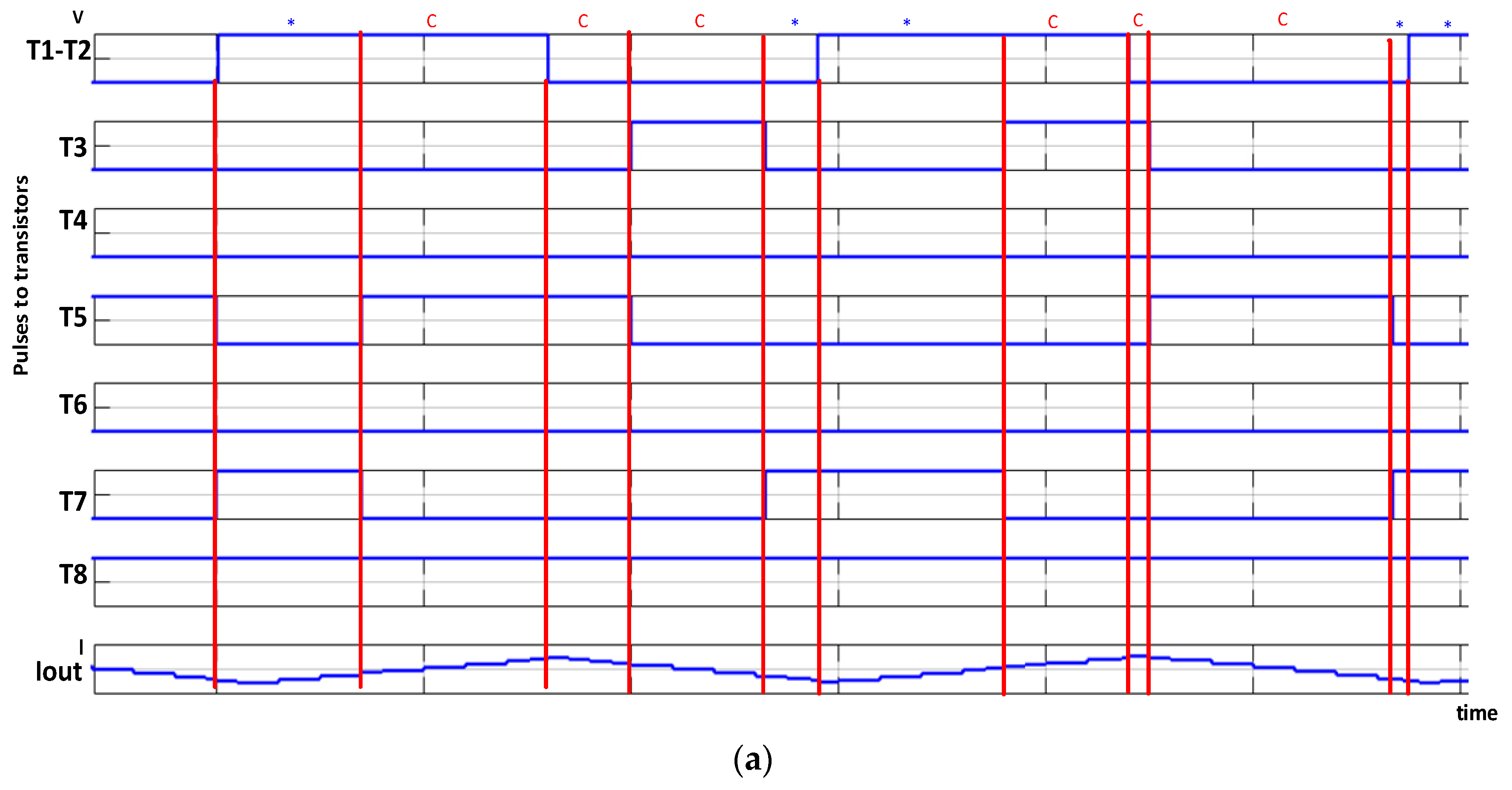
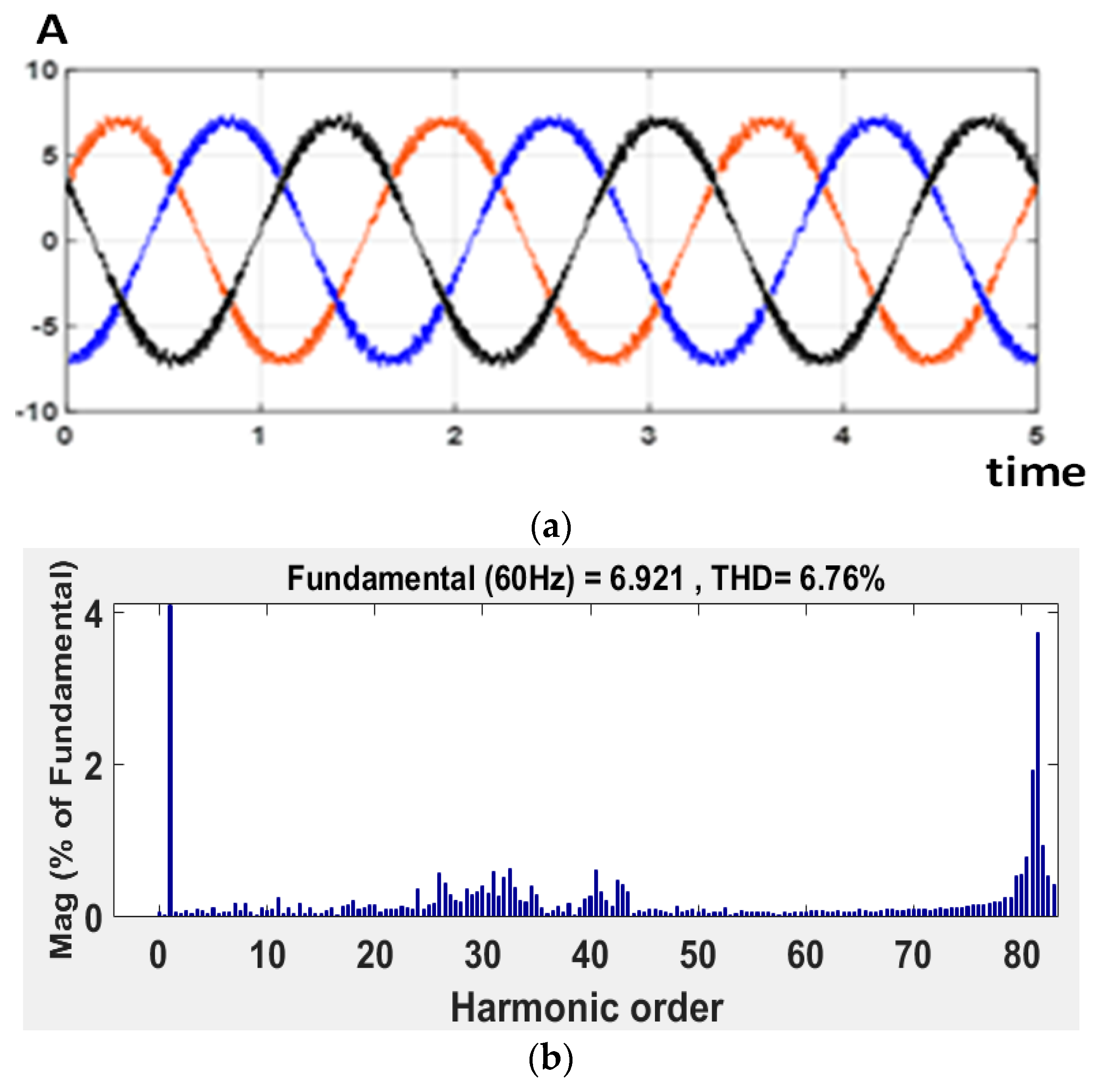
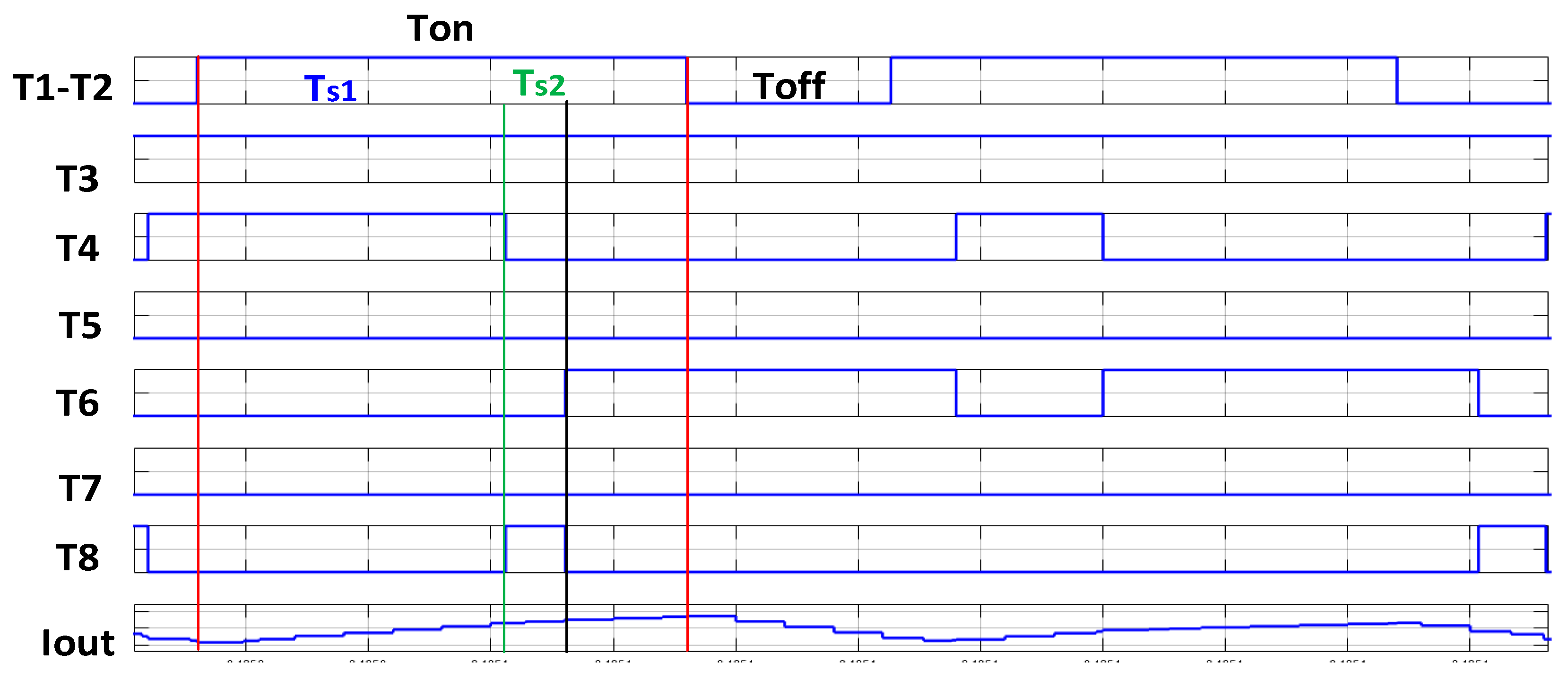
3.1. Technique of Modulation
3.2. Implementation of the Proposed Method
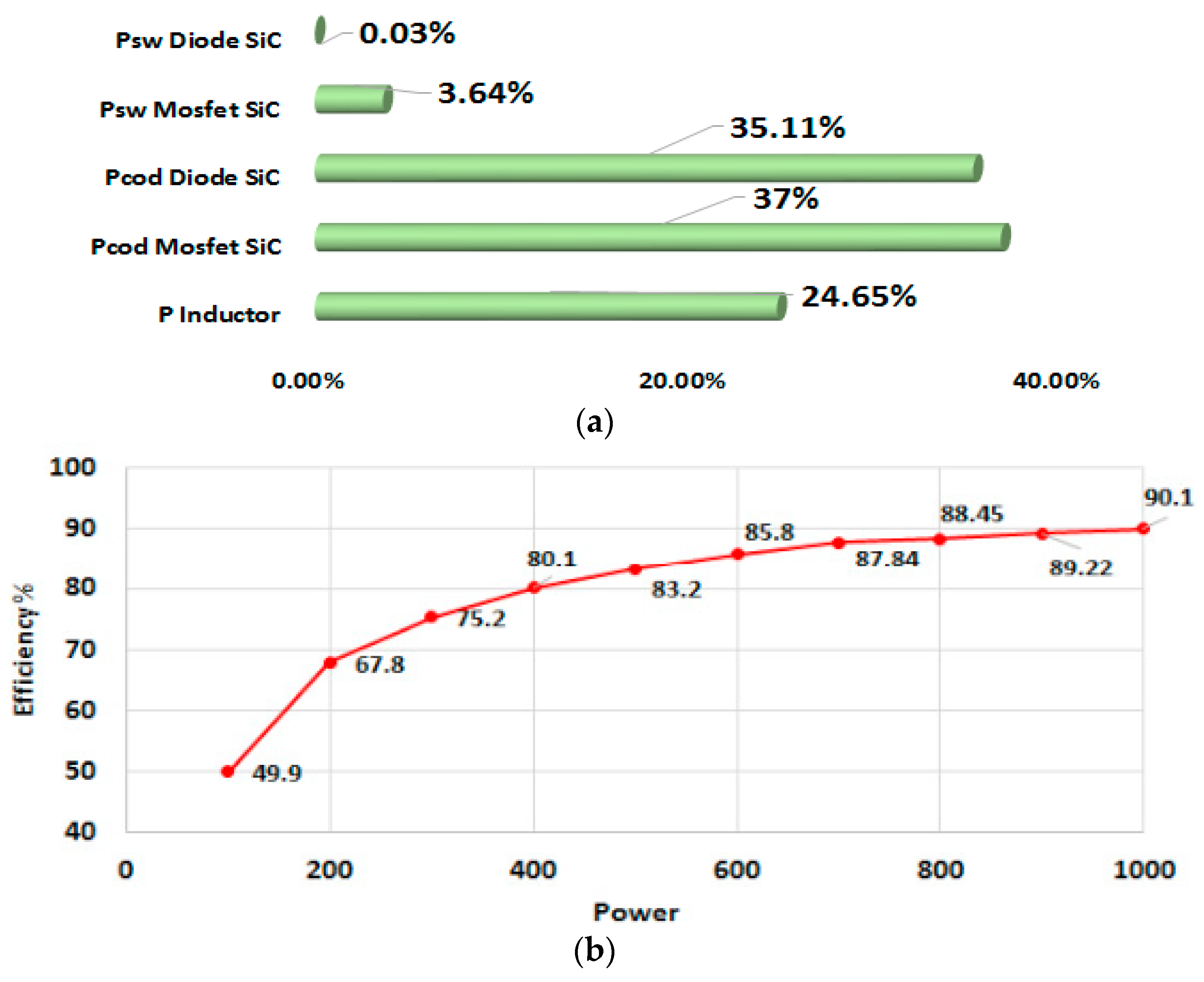
4. Analysis of Power Losses, Temperature and Efficiency
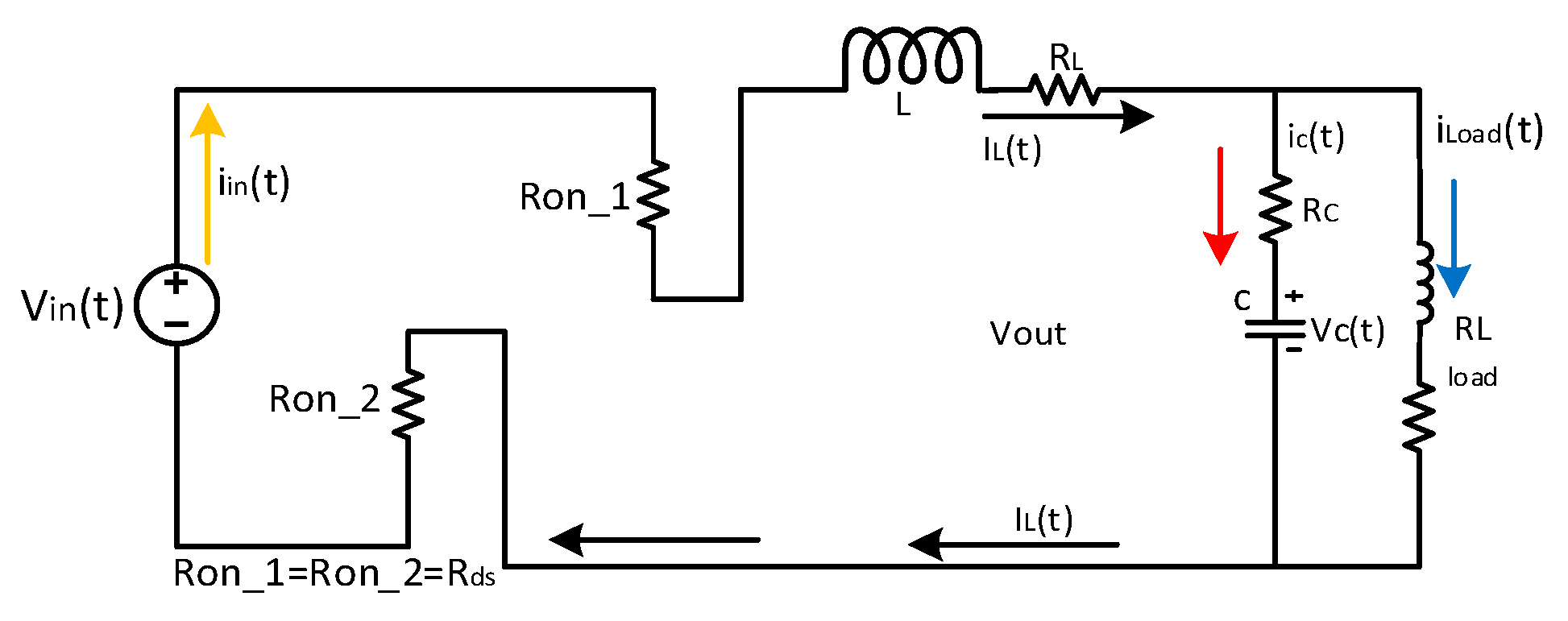
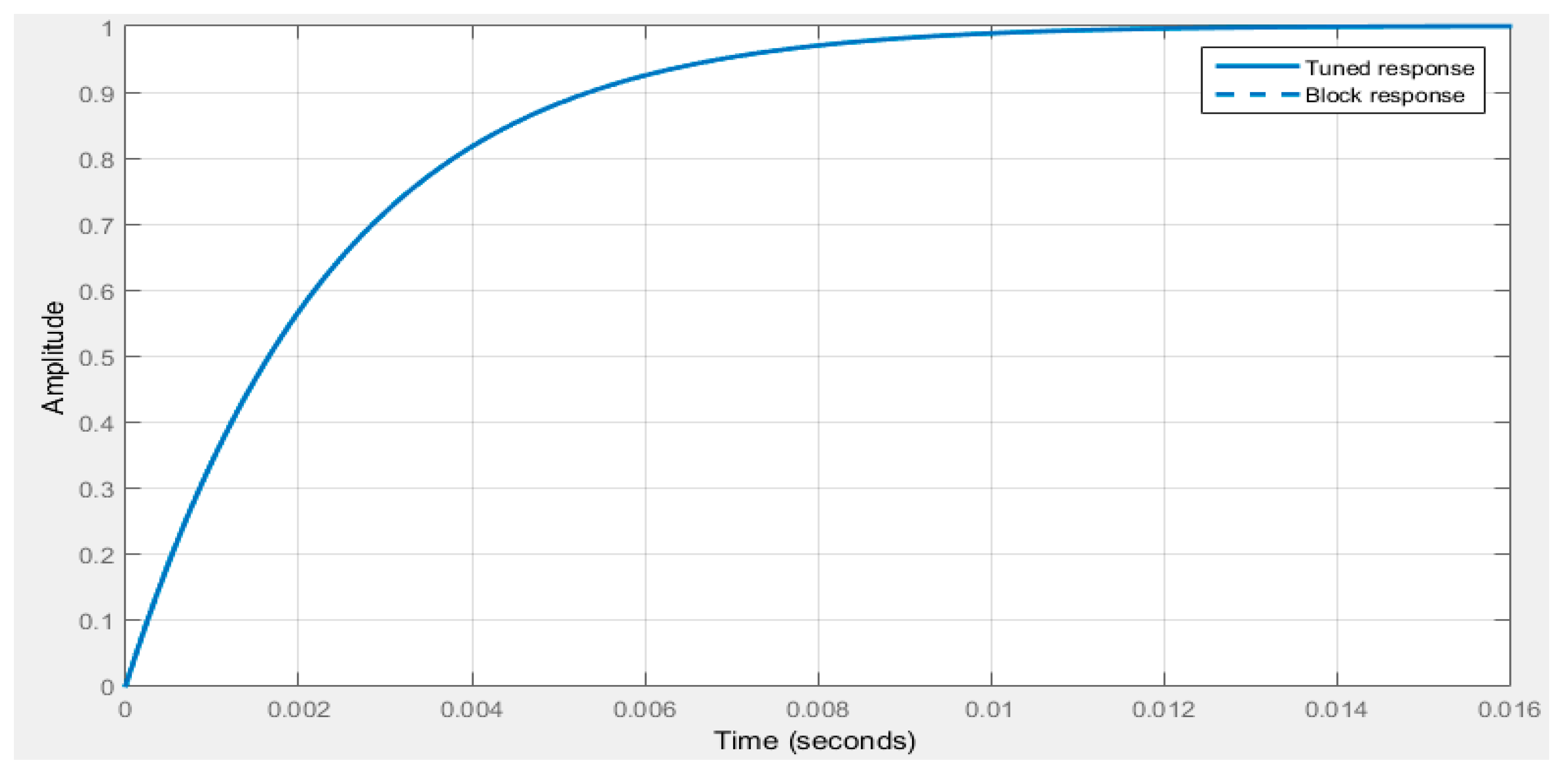
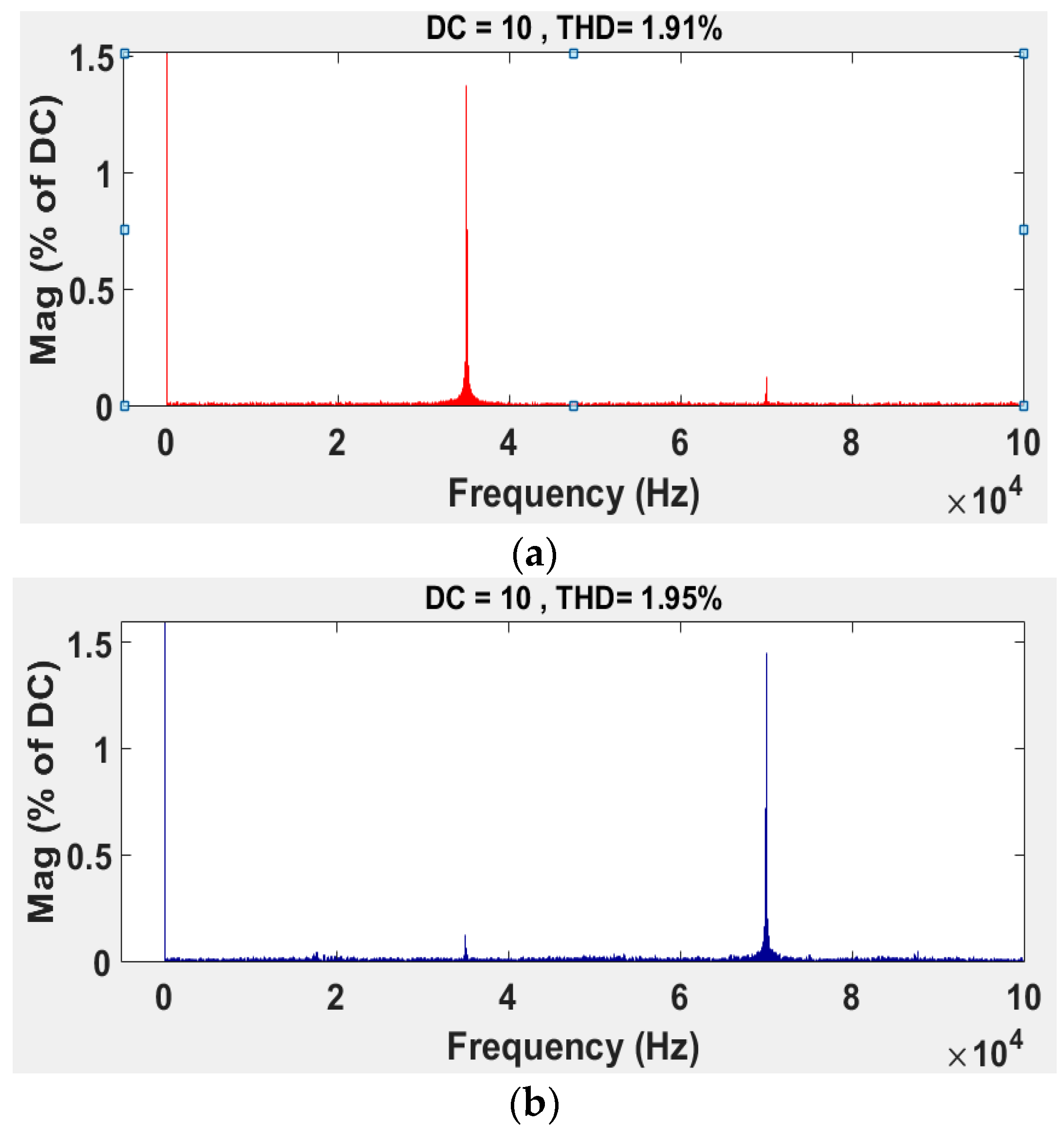
4.1. Power Losses and Efficiency in the V-I Power Converter
4.2. Inductor Core Losses
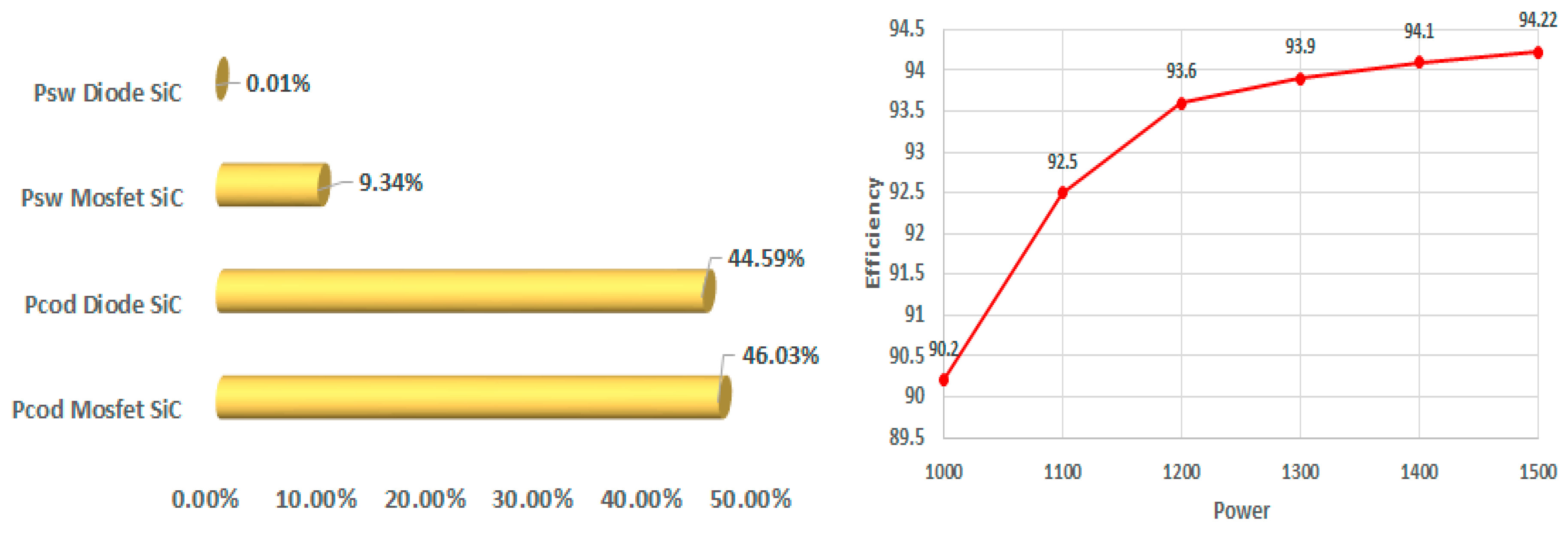
4.3. Power Losses and Efficiency in the Current Source Inverter
4.4. Power Losses in the Electric Motor
4.5. Heatsink Estimation
5. Conclusions
Author Contributions
Funding
Acknowledgments
Conflicts of Interest
References
- Bindra, A. Wide-Bandgap Power Devices: Adoption Gathers Momentum. IEEE Power Electr. Mag. 2018, 5, 22–27. [Google Scholar] [CrossRef]
- Choi, H. Overview of silicon carbide power devices. Fairchild Semicond. 2016, I, 1–6. [Google Scholar]
- She, X.; Huang, A.Q.; Lucía, Ó.; Ozpineci, B. Review of silicon carbide power devices and their applications. IEEE Trans. Ind. Electr. 2017, 64, 8193–8205. [Google Scholar] [CrossRef]
- Shang, F.; Arribas, A.P.; Krishnamurthy, M. A comprehensive evaluation of SiC devices in traction applications. In Proceedings of the 2014 IEEE Transportation Electrification Conference and Expo (ITEC), Dearborn, MI, USA, 15–18 June 2014; pp. 1–5. [Google Scholar]
- Merkert, A.; Müller, J.; Mertens, A. Component design and implementation of a 60 kW full SiC traction inverter with boost converter. In Proceedings of the Energy Conversion Congress and Exposition (ECCE), Milwaukee, WI, USA, 18–22 September 2016; pp. 1–8. [Google Scholar]
- Attia, Y.; Abdelrahman, A.; Hamouda, M.; Youssef, M. SiC devices performance overview in EV DC/DC converter: A case study in a Nissan Leaf. In Proceedings of the 2016 IEEE Transportation Electrification Conference and Expo, Asia-Pacific (ITEC Asia-Pacific), Busan, Korea, 1–4 June 2016; pp. 214–219. [Google Scholar]
- Han, D.; Li, S.; Wu, Y.; Choi, W.; Sarlioglu, B. Comparative analysis on conducted CM EMI emission of motor drives: WBG versus Si devices. IEEE Trans. Ind. Electr. 2017, 64, 8353–8363. [Google Scholar] [CrossRef]
- Ding, X.; Cheng, J.; Chen, F. Impact of silicon carbide devices on the powertrain systems in electric vehicles. Energies 2017, 10, 533. [Google Scholar] [CrossRef]
- Abdelrahman, A.S.; Erdem, Z.; Attia, Y.; Youssef, M.Z. Wide Bandgap Devices in Electric Vehicle Converters: A Performance Survey. Can. J. Electr. Comput. Eng. 2018, 41, 45–54. [Google Scholar]
- Ozpineci, B.; Tolbert, L.M.; Islam, S.K.; Theiss, T.J. A parametric device study for SiC diodes in vehicular applications. IEEE Veh. Technol. Conf. 1999, 3, 1495–1499. [Google Scholar]
- Han, D.; Li, Y.; Sarlioglu, B. Analysis of SiC based power electronic inverters for high speed machines. In Proceedings of the 2015 IEEE Applied Power Electronics Conference and Exposition (APEC), Charlotte, NC, USA, 15–19 March 2015; pp. 304–310. [Google Scholar]
- Han, D.; Noppakunkajorn, J.; Sarlioglu, B. Comprehensive efficiency, weight, and volume comparison of SiC-and Si-based bidirectional DC–DC converters for hybrid electric vehicles. IEEE Trans. Veh. Technol. 2014, 63, 3001–3010. [Google Scholar] [CrossRef]
- Sasagawa, M.; Nakamura, T.; Inoue, H.; Funaki, T. A study on the high frequency operation of DC-DC converter with SiC DMOSFET. In Proceedings of the Power Electronics Conference (IPEC), Sapporo, Japan, 21–24 June 2010; pp. 1946–1949. [Google Scholar]
- Sarigiannidis, A.G.; Kladas, A.G. Switching frequency impact on permanent magnet motors drive system for electric actuation applications. IEEE Trans. Magn. 2015, 51, 1–4. [Google Scholar] [CrossRef]
- Emadi, A.; Williamson, S.S.; Khaligh, A. Power electronics intensive solutions for advanced electric, hybrid electric, and fuel cell vehicular power systems. IEEE Trans. Power Electr. 2006, 21, 567–577. [Google Scholar] [CrossRef]
- Su, G.J.; Ning, P. Loss modeling and comparison of VSI and RB-IGBT based CSI in traction drive applications. In Proceedings of the Transportation Electrification Conference and Expo (ITEC), Detroit, MI, USA, 16–19 June 2013; pp. 1–7. [Google Scholar]
- Gnanasambandam, K.; Rathore, A.K.; Edpuganti, A.; Srinivasan, D.; Rodriguez, J. Current-Fed multilevel converters: An overview of circuit topologies, modulation techniques, and applications. IEEE Trans. Power Electr. 2017, 32, 3382–3401. [Google Scholar] [CrossRef]
- Mohammadi, M.; Moghani, J.S.; Milimonfared, J. A Novel Dual Switching Frequency Modulation for Z-Source and Quasi-Z-Source Inverters. IEEE Trans. Ind. Electr. 2018, 65, 5167–5176. [Google Scholar] [CrossRef]
- Tang, L.; Su, G.J. Boost mode test of a current-source-inverter-fed permanent magnet synchronous motor drive for automotive applications. In Proceedings of the 2010 IEEE 12th Workshop on Control and Modeling for Power Electronics (COMPEL), Boulder, CO, USA, 28–30 June 2010; pp. 1–8. [Google Scholar]
- Su, G.J.; Tang, L. Current source inverter based traction drive for EV battery charging applications. In Proceedings of the Vehicle Power and Propulsion Conference (VPPC), Chicago, IL, USA, 6–9 September 2011; pp. 1–6. [Google Scholar]
- Su, G.; Tang, L. A Current Source Inverter Based Motor Drive for EV/HEV Applications; SAE Technical Paper 2011-01-0346. 2011. Available online: https://doi.org/10.4271/2011-01-0346 (accessed on 16 October 2018).
- Abdelsalam, A.K.; Massoud, A.; Darwish, A.; Ahmed, S. Simplified generic on-line PWM technique for single phase grid connected current source inverters. In Proceedings of the 2012 Twenty-Seventh Annual IEEE Applied Power Electronics Conference and Exposition (APEC), Orlando, FL, USA, 5–9 February 2012; pp. 1398–1403. [Google Scholar]
- Masoud, M.I.; Abdel-Khalik, A.S. Vector controlled five-phase PWM-CSI induction motor drive. In Proceedings of the Power Engineering, Energy and Electrical Drives (POWERENG), Istanbul, Turkey, 13–17 May 2013; pp. 258–264. [Google Scholar]
- Bierhoff, M.H.; Fuchs, F.W. Semiconductor losses in voltage source and current source IGBT converters based on analytical derivation. In Proceedings of the Power Electronics Specialists Conference, Aachen, Germany, 20–25 June 2004; pp. 2836–2842. [Google Scholar]
- Huynh, C.; Zheng, L.; Acharya, D. Losses in High Speed Permanent Magnet Machines Used in Microturbine Applications. J. Eng. Gas Turbines Power 2008, 131, 022301. [Google Scholar] [CrossRef]
- Guo, Q.; Zhang, C.; Li, L.; Zhang, J.; Liu, J.; Wang, T. Efficiency optimization control of permanent-magnet synchronous machines for electric vehicle traction systems. In Proceedings of the Vehicle Power and Propulsion Conference (VPPC), Hangzhou, China, 17–20 October 2016; pp. 1–5. [Google Scholar]
- Hassan, W.; Wang, B. Efficiency optimization of PMSM based drive system. In Proceedings of the 2012 7th International Power Electronics and Motion Control Conference (IPEMC), Harbin, China, 2–5 June 2012; pp. 1027–1033. [Google Scholar]
- Aguilar Gamarra, H.N. Design of a Synchronous Motor with Ferrite Magnets. Bachelor’s Thesis, Universitat Politècnica de Catalunya, Barcelona, Spain, 2014. [Google Scholar]
- Antonopoulos, A.; Bangtsson, H.; Alakula, M.; Manias, S. Introducing a silicon carbide inverter for hybrid electric vehicles. In Proceedings of the Power Electronics Specialists Conference 2008 (PESC 2008), Rhodes, Greece, 15–19 June 2008; pp. 1321–1325. [Google Scholar]


| Parameter | Values |
|---|---|
| Kp | 4.75769580834167 |
| Ki | 460.186624758197 |
| Rise time | 0.00488 s |
| Settling time | 0.00838 s |
| Overshoot | 0.0198% |
| Peak | 1 |
| Phase margin | 889 deg @ 439 rad/s |
| Parameter | Values |
|---|---|
| Vdc | 100 V |
| Current | 10 A |
| Inductor L1 | 10 mH |
| Frequency Fs | 35 kHz |
| Capacitor C1, C2, C3 | 1 5 μF |
| Index of Modulation m | 0.8 |
| L Load | 1.5 mH |
| R Load | 1.3 Ω |
| Angle of Shift | Values of THD | Sequence ON OFF |
|---|---|---|
| 0° | 2.10% | C*CC*CC|C*CC*CC |
| 30° | 2.22% | CC*CC*C|CC*CC*C |
| 60° | 2.39% | *CC*C*C|*CC*C*C |
| 90° | 1.98% | C*CC*CC|C*CC*CC |
| 120° | 2.25% | *CC*CC*|*CC*CC* |
| 150° | 2.13% | C*CCC*C|C*CCC*C |
| 180° | 2.15% | CC*C*CC|CC*C*CC |
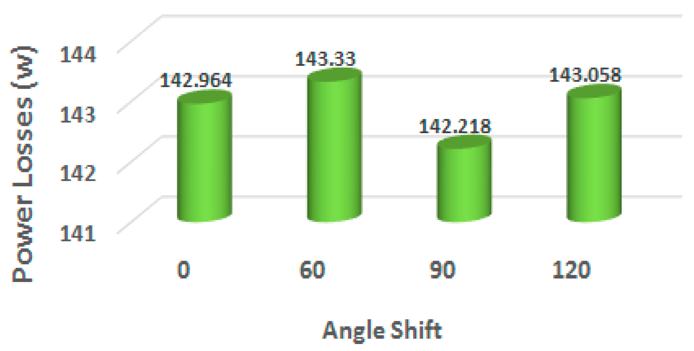
| Shift-Angle | Values of THD |
|---|---|
| 0° | 2.29% |
| 90° | 2.74% |
| 120° | 2.45% |
| Parameter | Mosfet SiC | Parameter | Diode SiC |
|---|---|---|---|
| Model | SCT2450KE | Model | C3D10065I |
| Voltage DS | 1200 V | VRRM (V) | 650 V |
| Current | 10 A | QC (nC) | 110 nC |
| Rds | 450 mΩ | IF (A) | 10 A |
| Power Dissipation | 85 W | ||
| Operating Junction | 175 °C |
| Parameter | Value |
|---|---|
| Hysteresis losses | 0.0517 W/cm3 |
| Eddy current losses | 0.2738 W/cm3 |
| Copper losses | 29.93 W/cm3 |
| Total of losses in the inductor | 30.255 W/cm3 |
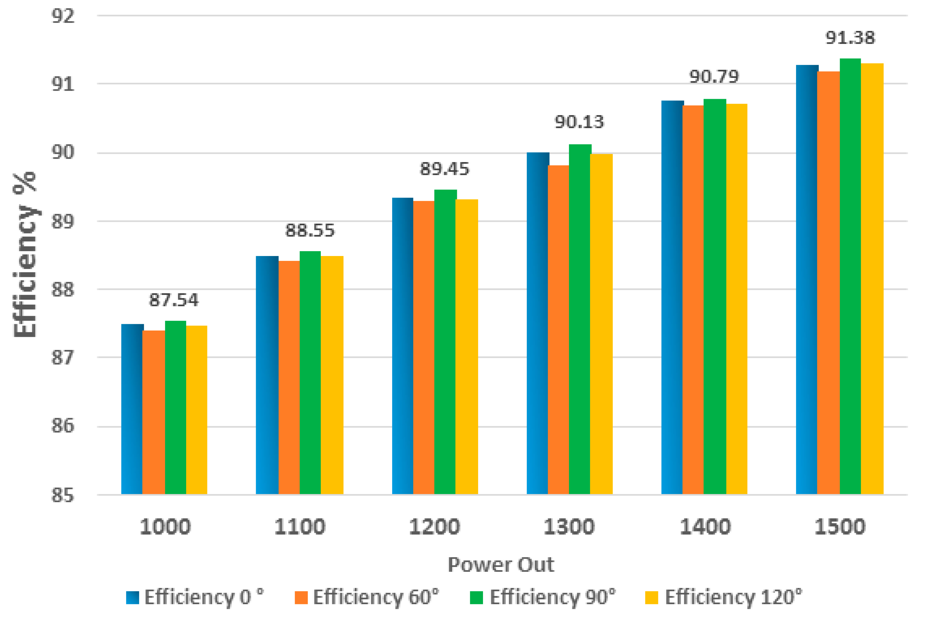
| System | Efficiency at 0° | Efficiency at 90° | Power Out |
|---|---|---|---|
| V-I | 88.25% | 90.1% | 1 kW |
| CSI | 93.8% | 94.22% | 1.5 kW |
| Motor | 91.2% | 91.38% | 1.5 kW |
| Average | 91.08% | 92% | 1.5 kW |
| Parameter | Mosfet SiC | Parameter | Diode SiC |
|---|---|---|---|
| Model | HGTG30N60BD3 | Model | C3D10065I |
| Voltage CE | 600 V | VRRM (V) | 650 V |
| Current | 15 A | QC (nC) | 110 nC |
| Power Dissipation | 208 W | IF (A) | 10 A |
| Operating Junction | 150 °C |
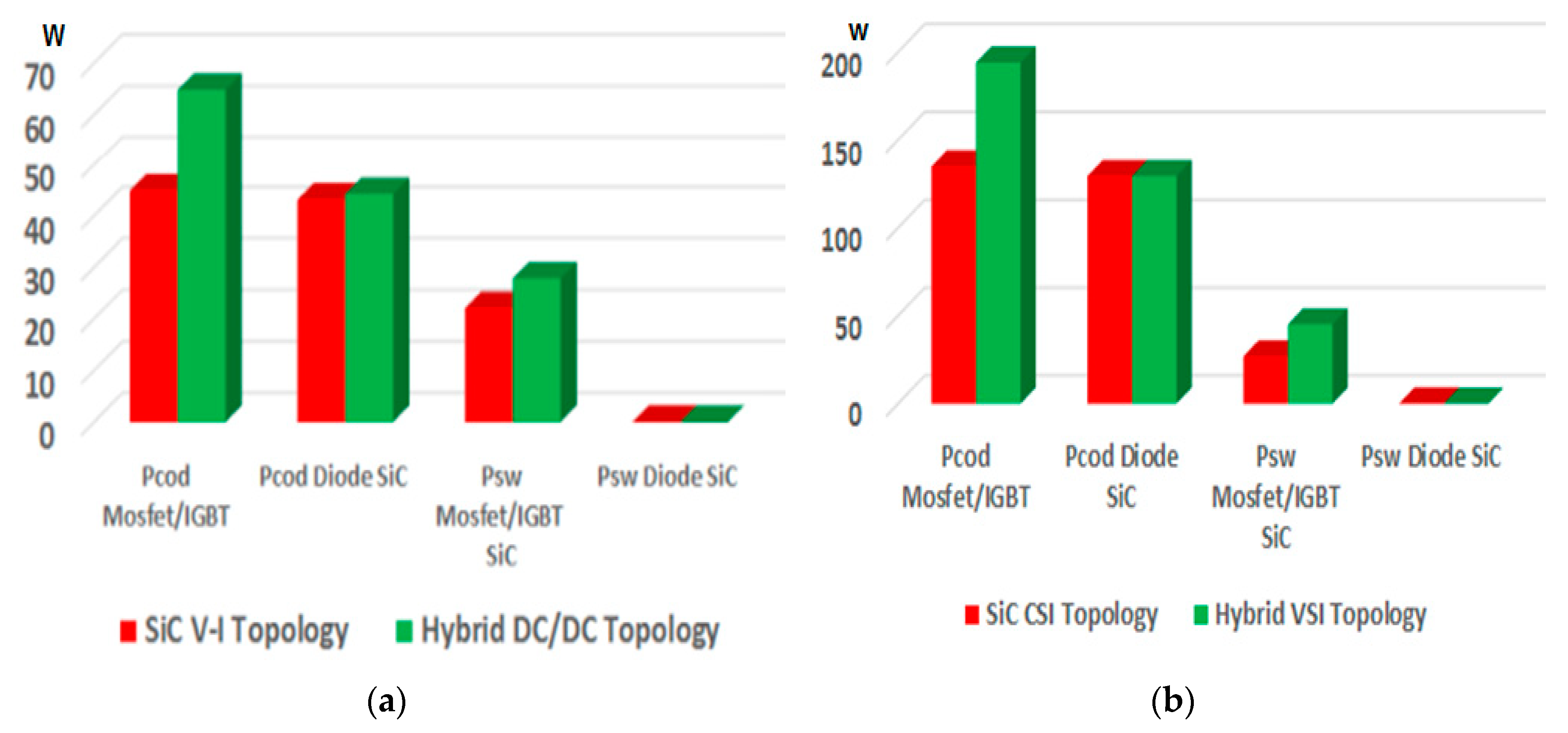
| Parameter | All-SiC Topology V-I–CSI | Hybrid Topology DC/DC–VSI | ||
|---|---|---|---|---|
| Pconduction Mosfet SiC/IGBTs | 44.98 W | 134.94 W | 64.9 W | 194.24 W |
| Pconduction diodes | 43.16 W | 129.48 W | 44.57 W | 129.42 W |
| Pswitching SiC/IGBTs | 22.87 W | 26.88 W | 27.88 W | 45.08 W |
| Pswitching diodes | 0.0296 W | 0.178 W | 0.0006 W | 0.036 W |
| Total | 402.51 W | 506.29 W | ||
© 2018 by the authors. Licensee MDPI, Basel, Switzerland. This article is an open access article distributed under the terms and conditions of the Creative Commons Attribution (CC BY) license (http://creativecommons.org/licenses/by/4.0/).
Share and Cite
Fernández, E.; Paredes, A.; Sala, V.; Romeral, L. A Simple Method for Reducing THD and Improving the Efficiency in CSI Topology Based on SiC Power Devices. Energies 2018, 11, 2798. https://doi.org/10.3390/en11102798
Fernández E, Paredes A, Sala V, Romeral L. A Simple Method for Reducing THD and Improving the Efficiency in CSI Topology Based on SiC Power Devices. Energies. 2018; 11(10):2798. https://doi.org/10.3390/en11102798
Chicago/Turabian StyleFernández, Efrén, Alejandro Paredes, Vicent Sala, and Luis Romeral. 2018. "A Simple Method for Reducing THD and Improving the Efficiency in CSI Topology Based on SiC Power Devices" Energies 11, no. 10: 2798. https://doi.org/10.3390/en11102798
APA StyleFernández, E., Paredes, A., Sala, V., & Romeral, L. (2018). A Simple Method for Reducing THD and Improving the Efficiency in CSI Topology Based on SiC Power Devices. Energies, 11(10), 2798. https://doi.org/10.3390/en11102798