1. Introduction
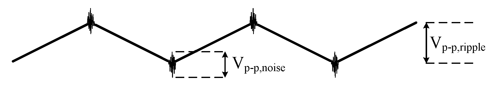
With the increasingly stringent requirements on the output quality of instrument power supplies, the switching noise imposed on the output voltage should be minimized. Conventional linear regulators have excellent performance in terms of the noise concern, but cannot handle high power due to efficiency problems and the inability to process bidirectional power flow. Switching power converters, on the contrary, are capable of improving efficiency at high power outputs; the switching actions induce switching noise on the output and degrade the power quality of the load. The high-frequency switching noise usually ranges over a few hundred kHz to several MHz. The voltage perturbation is illustrated as in
Figure 1.
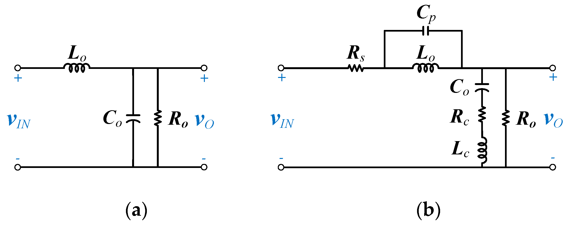
There are two factors influencing the switching noise in a switching power supply: one is the non-ideal characteristic of the output filter, and the other is the high-frequency component spectra of the voltage waveform injecting into the filter. Firstly, dealing with the non-ideal characteristics of the filter, take a buck converter as an example. The output inductor and capacitor are not only used to store energy, but also behave as a filter to reduce the output ripple. An ideal LC low-pass filter, as shown in
Figure 2a, can completely filter out the high-frequency component well above the designed cut-off frequency. However, practical inductors and capacitors contain parasitic elements. The parasitic elements in an inductor contains the capacitance between the windings as well as between the winding conductor and the core, denoted as lumped capacitance,
Cp. In addition, there is winding equivalent resistance,
Rs, as shown in
Figure 2b. As for the capacitor counterpart, it contains the equivalent series inductance,
Lc, and equivalent series resistance,
Rc. These parasitic elements alter the transfer function of the filter and deteriorate the capability to filter out high frequency signals.
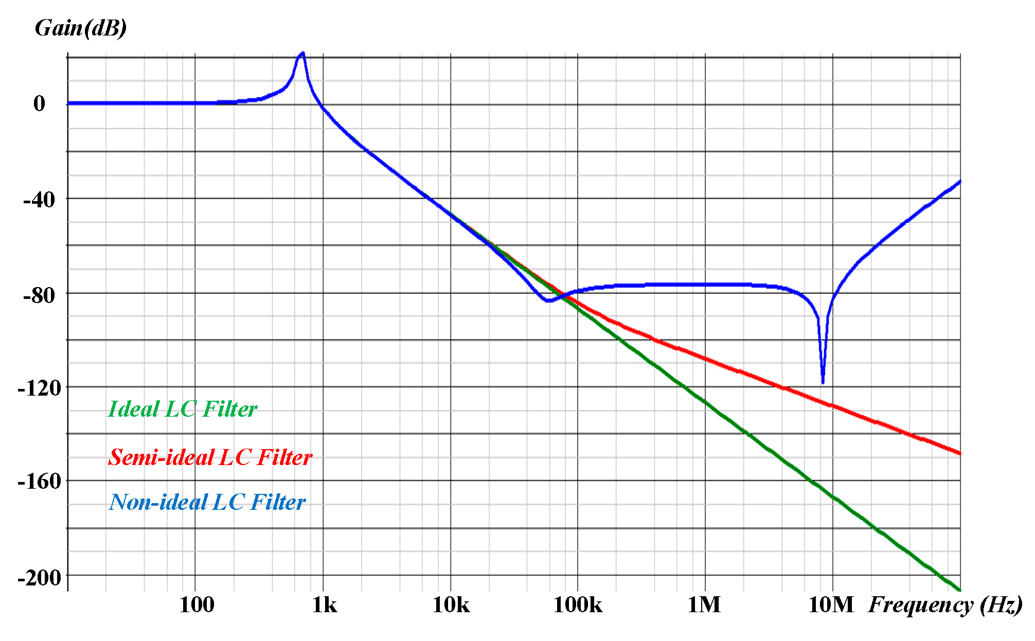
Figure 3 shows the bode plots of ideal, semi-ideal and non-ideal filters. The component parameters used in the figure are as follows:
Lo = 42 μH,
Rs = 0 Ω,
Cp = 10 pF,
Co = 1.36 mF,
Rc = 1 mΩ,
Lc = 6 μH,
Ro = 10 Ω. Where
Co is the filter capacitor,
Lo is the filter inductor,
Ro is the load resistor,
vIN is the input voltage, and
vo is the output voltage. The semi-ideal filter only considers the capacitor’s equivalent series resistance (
ESR), the extra zero brings about +20 dB/dec; on the other hand, the non-ideal filter considers all the parasitic components; even a +40 dB/dec slope is present at extremely high-frequency regions. In other words, the high-frequency components of the input signal will be detected at the output terminals.
Clearly, it is very difficult to reduce the parasitic components on the filter; practically, it is impossible to eradicate them. Elsewise, in order to counteract the high-frequency current generated by the parasitic capacitance on the inductor, the literature [
1] proposes an external circuit. The inductor is connected in parallel to a transformer or a secondary side winding, and a compensating capacitor is connected in series to the secondary side. By adjusting the transformer turns ratio to produce an appropriate compensating current, the transient current evoked from the parasitic capacitance is neutralized. Although the method claims limited extra circuitry components or volume/weight required to depress the switching noise, its performance will be seriously impaired due to the inevitable leakage inductance accompanying the additionally coupled winding, which is not accounted for in the theory. Another paper [
2] proposed a different improved compensation circuit to reduce the effect of leakage inductance. In this external circuit, the compensation capacitor is connected to both sides of the extra coupled inductor, and the effect of leakage inductance will be greatly reduced. For both of the above methods, an accurate inductor parasitic capacitance value is indispensable. However, this itself is a difficult task. Many researchers endeavor to construct inductor parasitic capacitance models and several parameter assignments have been proposed [
1,
2,
3], even though the thickness, pitch or tightness deviation of the winding under realistic industrial mass production will affect the parasitic capacitance. Neither way is appropriate to reliably compensate for all the products under mass production.
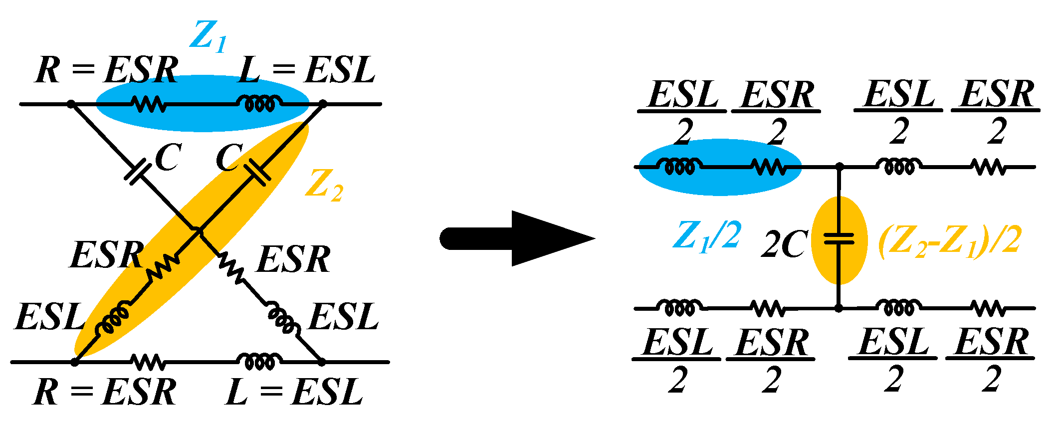
On the other hand, elimination of parasitic inductance on the output capacitor is another remedy for reducing the high-frequency voltage noise. Reference [
3] proposes a technique for eliminating the capacitor’s equivalent series inductance (
ESL) and
ESR.
As shown in
Figure 4, the two non-ideal capacitors are connected in diagonal form. From circuit theorem, if the compensation impedance
Z1 is equal to that of
ESL and
ESR, there is an equivalent pure capacitance located in the middle point. For high-frequency signals, the inductor exhibits high impedance while the capacitor exhibits low impedance. Therefore, the high-frequency noise can no longer pass through to the output. Although the compensation impedance
Z1 in this method is of limited value and can be implemented by using printed circuit board (PCB) trace, the internal parasitic elements inside capacitors are divergent due to several reasons. Therefore, there are still many difficulties to solve before mass production is possible. Nevertheless, the tolerance allowed for this method is wider than the compensation of inductor parasitic capacitance methods.
Since the elimination of parasitic components in a filter circuit is very difficult, the remnant prescription is to reduce the voltage transient across the inductor. The commonly developed ZVS techniques indeed reduce the voltage transient since the inductor voltage transits over a longer commutation time as the switch voltage falls to zero. This simple idea just launches a much wider possibility for switching noise alleviation.
A synchronous rectified step-down converter operated in the triangular-current mode (TCM) [
4,
5,
6] is a common way to achieve ZVS without introduction of auxiliary resonant components. For TCM operation, the inductor current is usually designed to operate in boundary conduction mode (BCM) at full load; therefore, TCM can be assured under the entire load range. However, this means that the inductance should be small so that the peak inductor current doubles the output current at full load. This seriously impairs the converter efficiency, especially at light load.
There are many proposed ZVT converters with auxiliary switches or resonant circuitry to achieve ZVS benefits [
7,
8,
9,
10,
11]. However, the ZVS feature cannot be maintained within the overall load and voltage range. In recent years, the literature [
12,
13,
14,
15] lists many novel bidirectional converters applying various methods to achieve soft switching. However, most of them suffer from the range limitation of ZVS, i.e., ZVS is only achievable within a small range of load level, or even output voltage in some applications. A method proposed in [
16] is capable of retaining ZVS switching at any load and wide output voltage range while reducing the switching losses of the auxiliary switch by a coupled inductor. However, from the detailed discussion in the next section, it is clear that the output switching noise could be further reduced if soft switching of switching-off is considered. Unfortunately, the aforementioned papers only focus on ZVS turn-on; i.e., those methods only alleviate the rising slope of the filter input voltage, but without solving the sharp noise of the falling edge. In this paper, a new circuit architecture is proposed to achieve bilateral ZVS over a wide load range and wide output voltage. This architecture can reduce the output switching noise by controlling the resonant capacitor to simultaneously adjust the rise and fall slope of the voltage across the main switch. The voltage change rate of these is the same and does not change with the output voltage and the output current. It is not necessary to detect the voltage signal to determine the opening timing of the main switch, which is beneficial to the application of high-frequency switching. This architecture is especially suitable for instrument power which characterizes the low switching noise trait over wide load/voltage range.
The remaining arrangement of this paper is as follows:
Section 2 discusses the Fourier analysis of the filter’s input voltage.
Section 3 shows the structure and operation principle of the proposed circuit. Detailed analyses of the circuit and the requirement for ZVS are described in
Section 4.
Section 5 is about the design consideration and equations of this architecture.
Section 6 presents the simulation and measured results to verify the correctness and feasibility. Finally, the conclusion follows.
2. Fourier Analysis on Filter Input Voltage Waveforms
As for the discussion on the influence of frequency spectra of the input voltage waveform, take a buck converter as an example again. Ideally, the voltage at the LC filter’s input port is a rectangular waveform. From the definition of the Fourier series, the Fourier series expansion of a rectangular waveform,
frect(
t) is:
where
Practically, there is always a small rise/fall time in the waveform. To simplify the analysis, let us assume an identical rise and fall time,
tr/
tf. Then we have a trapezoidal waveform. By dissecting the waveform into a rectangle and two triangles, the Fourier series expansion of a trapezoidal waveform,
ftrap(
t) is:
where
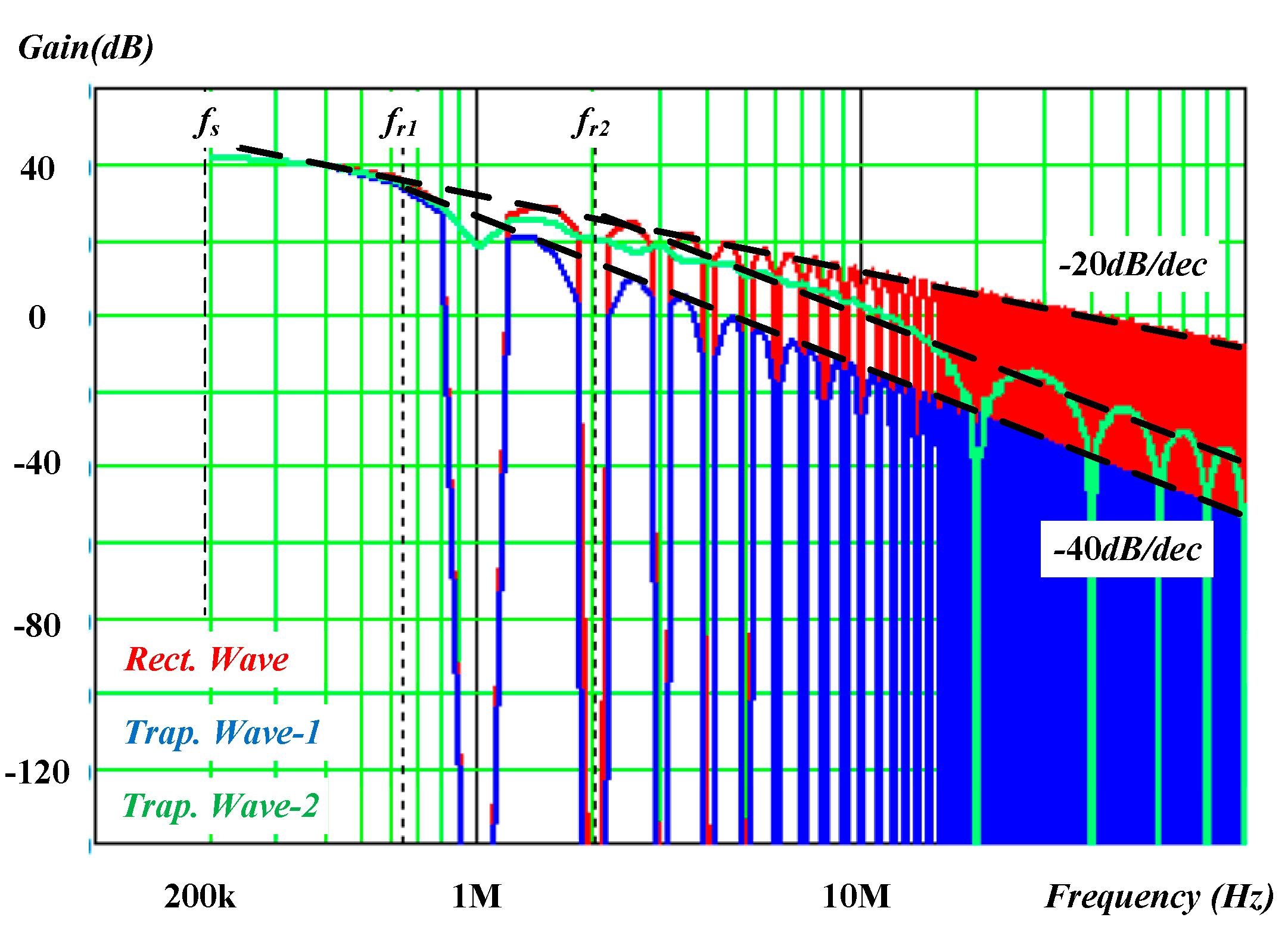
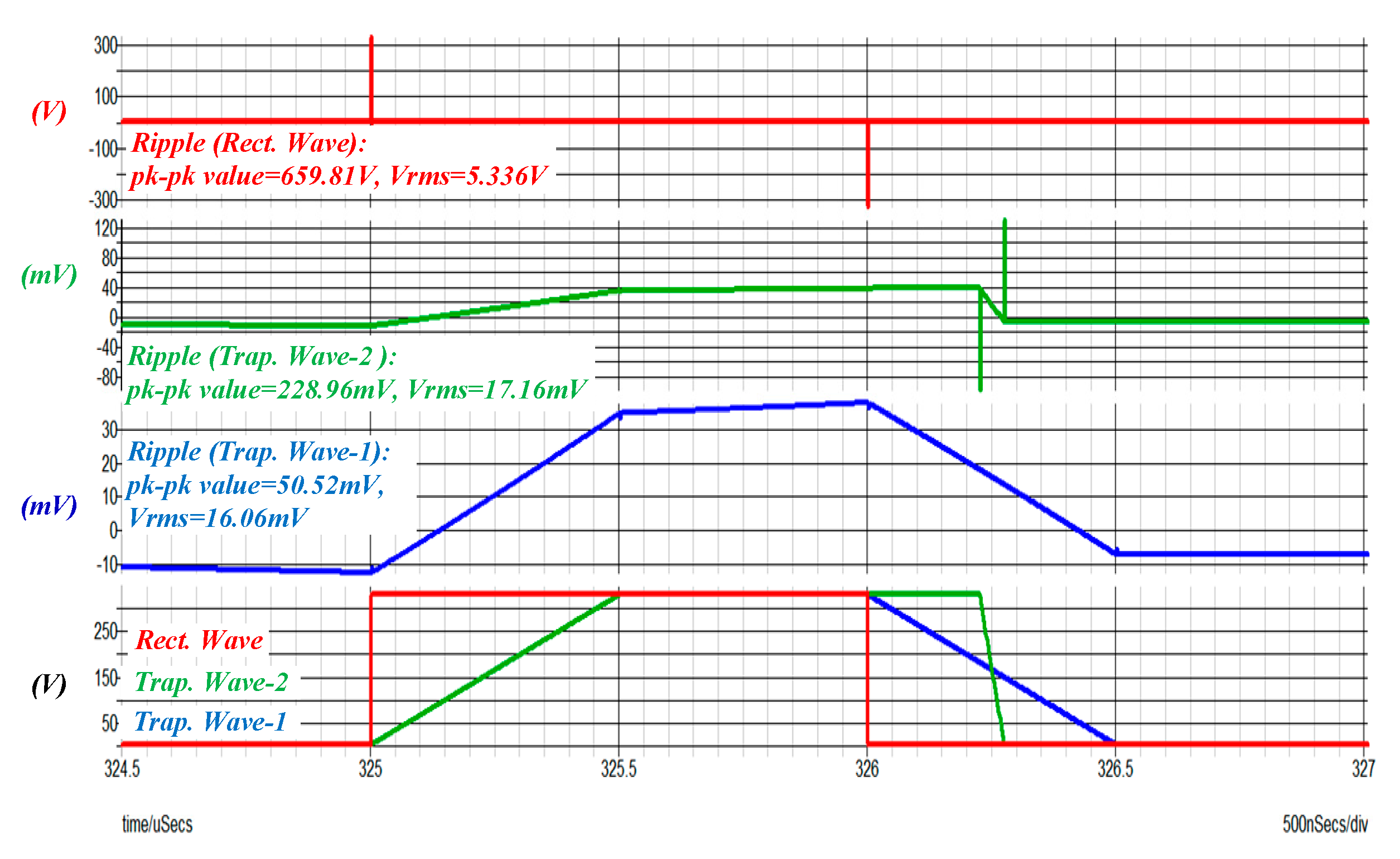
Figure 5 is the Fourier spectrum of a rectangular and two trapezoidal waveforms. “Rect. Wave” represents a rectangular waveform, “Trap. Wave-1” represents a trapezoidal waveform of
tr =
tf = 500 ns, and “Trap. Wave-2” represents a trapezoidal wave of
tr = 500 ns,
tf = 50 ns. The amplitudes of the three waveforms are all 300 V, the equivalent duty ratio is 0.2, and the switching frequency is 200 kHz. The rectangular wave’s spectrum turning point is the switching frequency. After the switching frequency, the maximum value of each harmonic decreases with a slope of −20 dB/dec. However, there are two turning points in the trapezoidal waveform’s spectrum: one is the switching frequency
fs, and the other is
fr*, which is the control by the trapezoidal wave. Beyond the
fr frequency (
), the maximum value of each harmonic decreases with a slope of −40 dB/dec. If the slope of the rising and falling of a trapezoidal wave can be properly designed, the high frequency component will be rapidly attenuated after a suitable frequency. Even with non-ideal LC filters, the high-frequency components of the output voltage can still be properly attenuated.
From the time-domain analysis, slowing down the voltage variation slope also reduces the instantaneous charging current
iCp of the parasitic capacitance
Cp of the non-ideal LC filter in
Figure 2b.
Figure 6 shows the simulation results for the three kinds of input voltage waveforms used in
Figure 5 fed into the non-ideal LC filter respectively. The results show that the rectangular waveform generates the maximum switching noise in both root mean square (rms) and peak–peak values. A trapezoidal waveform with alleviated rising slope did prove attenuated switching noise; however, high switching noise was still present due to the steep falling edge. The bilateral trapezoidal one that slows down both the rising and falling slopes has the smallest switching noise.
3. Circuit Topology and Operation Principle
Figure 7 shows the proposed bilateral ZVS synchronous rectified step-down converter. The main switches
Qsr1 and
Qsr2 cooperate with the output inductor
Lo and the output capacitor
Co to form a conventional synchronous rectified step-down converter. In order for the high-side switch to achieve ZVS,
CossQsr1 must be completely discharged before
Qsr1 is turned on. To achieve this purpose, a resonant inductor
Lr is added to supply the discharging current at suitable timing. The bidirectional switch
Qaux is turned on shortly before the turn-off of
Qsr1/
Qsr2, and is turned off after
Qsr1/
Qsr2 is turned on. The turn-on of
Qaux will create a charging path for
Lr to generate the current required for ZVS operation. C
ossD1/C
ossD2 represents the sum of the applied capacitance of the diode
D1/
D2 and its own parasitic capacitance.
Cr1 is the sum of
CossD1 and
CossQsr1, and
Cr2 is the sum of
CossD2 and
CossQsr2.
CossD1 and
CossD2 are much larger than the parasitic output capacitance of
Qsr1,
Qsr2,
Q1 and
Q2. By adjusting
Cr1,
Cr2 and the resonant inductor
Lr, the voltage transition rate across the switches,
Qsr1 and
Qsr2, as well as the resonant current magnitude can be adjusted.
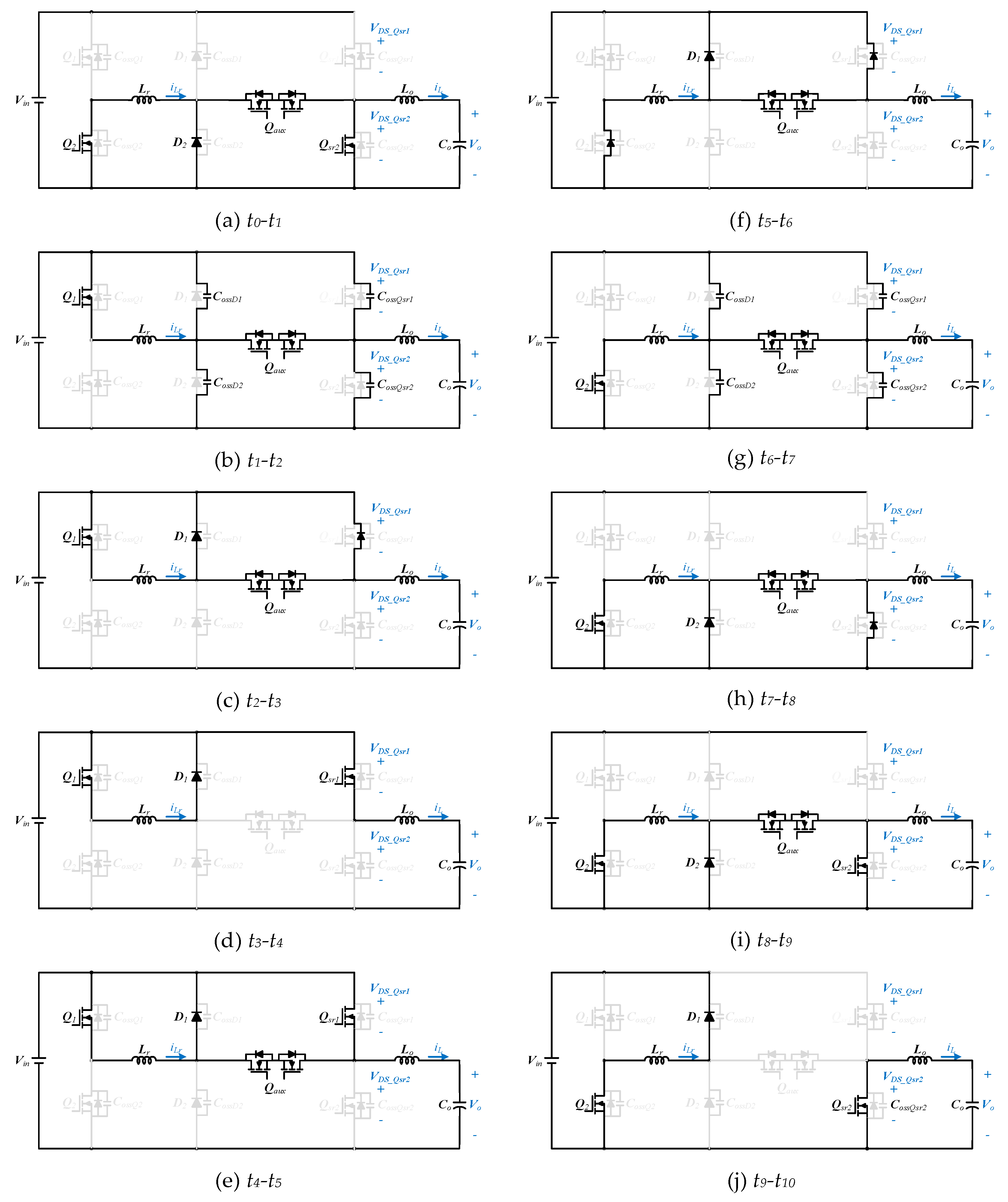
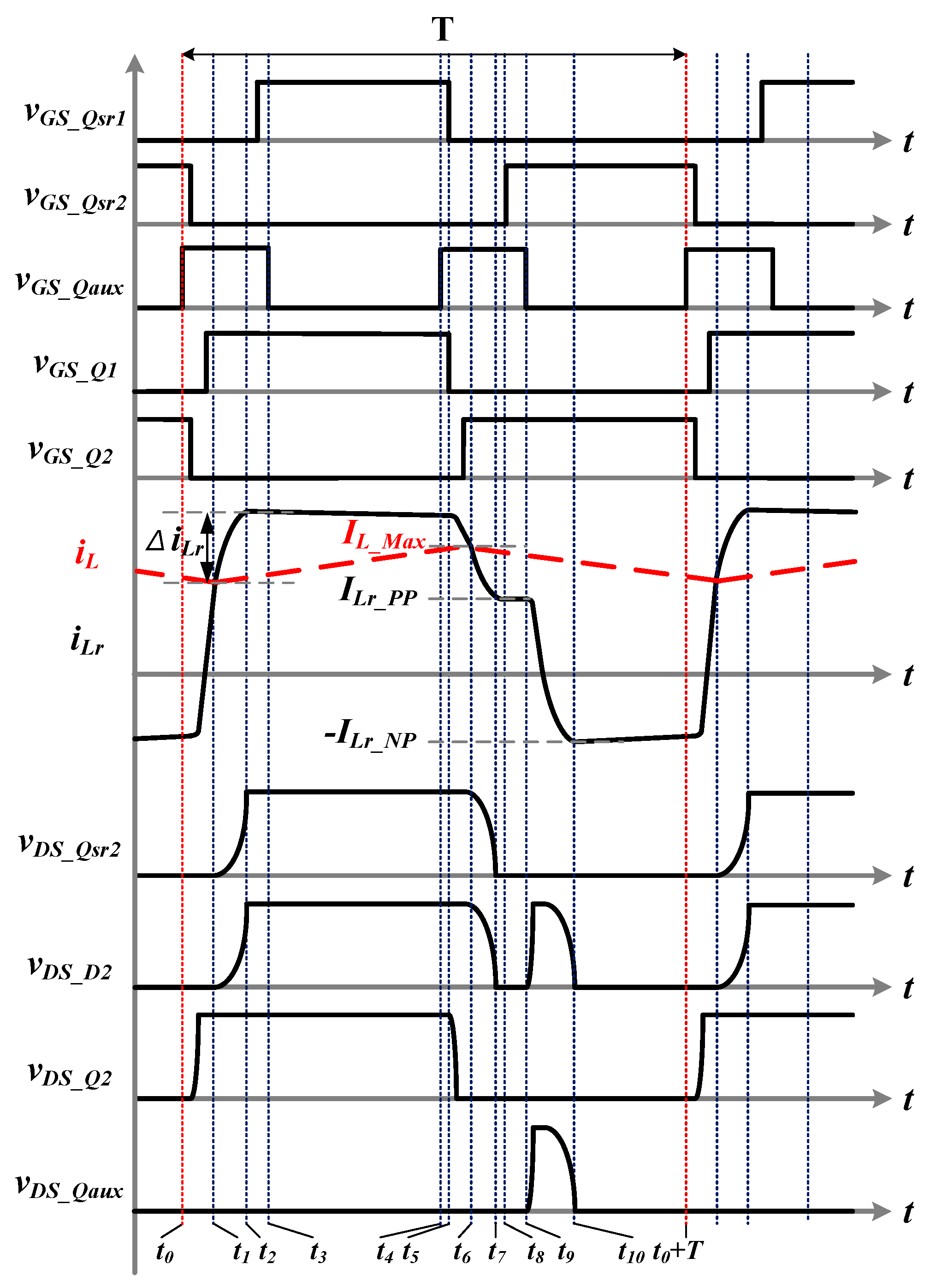
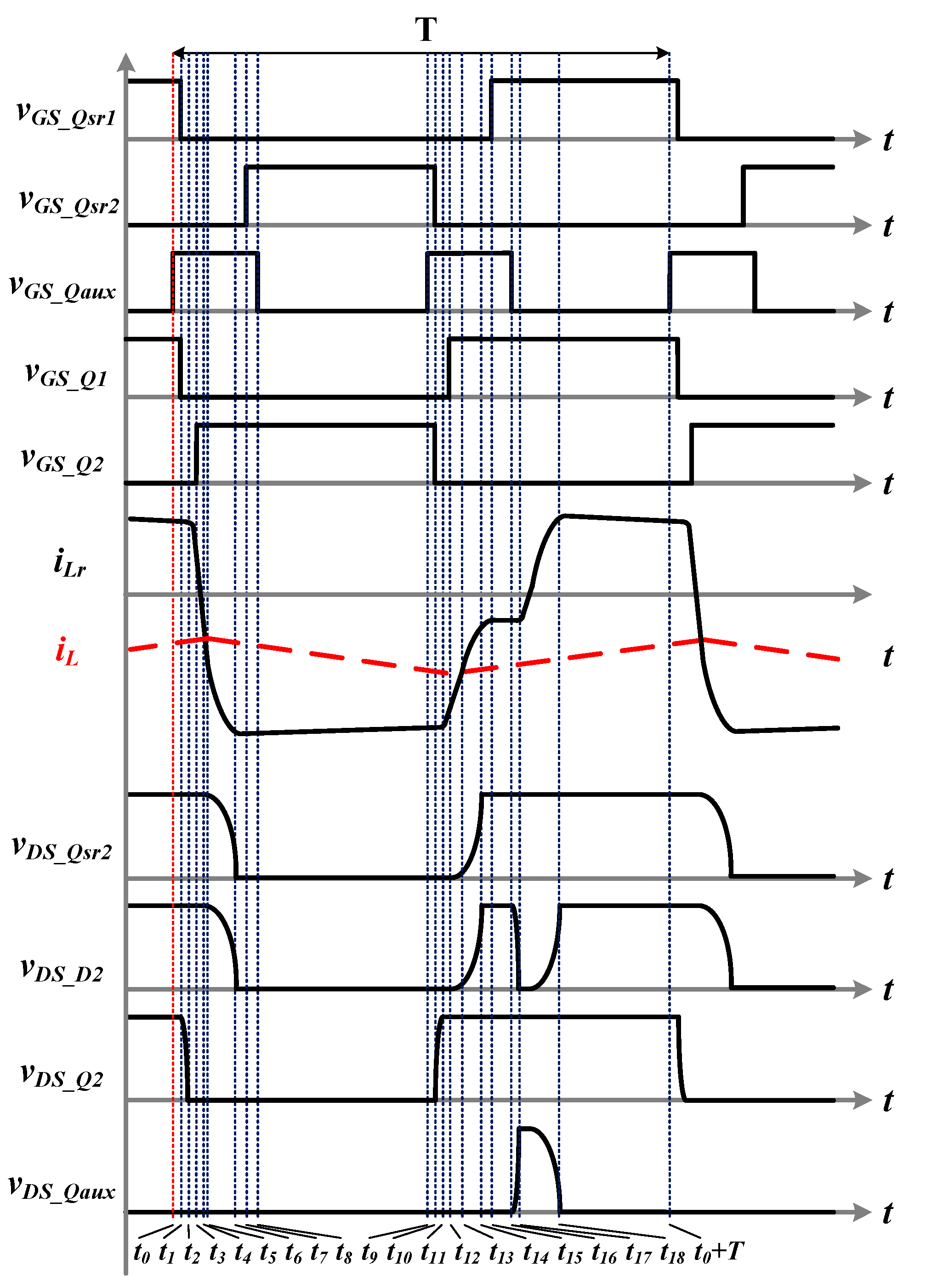
This architecture can be a bidirectional topology that uses the same switching signal to achieve natural commutation, and forward and reverse operation has similar behavior. This paper gives a detailed explanation of the forward operation, and the reverse part is presented with an action timing diagram. The complete circuit operation can be divided into 10 intervals as described later. The theoretical waveforms of forward mode are depicted in
Figure 8, while the corresponding circuit operation diagrams are illustrated in
Figure 9. Due to the length limitation, this paper does not elaborate on the action intervals of the reverse power flow operation. A timing diagram,
Figure 10, is attached to illustrate the reverse power flow operation as a reference. For the convenience of analysis, the resonant capacitors
Cr1 and
Cr2 are assumed to be identical, i.e.,
Cr1 =
Cr2 =
Cr.
Interval 1 (t0–t1): Before t0, switches Q2 and Qsr2 are conducting. The output inductor current keeps flowing through Qsr2, and the resonant current iLr freewheels through D2. Therefore, the voltage across Qaux is zero, and vGS_Qaux can be pulled high at t0 to turn on Qaux at zero voltage. Shortly following the turn-on of Qaux, Q2 is turned off. After Q2 is turned off, the resonant current detours to the body diode of Q1. Since the voltage across the resonant inductor is Vin, the resonant inductor current rises linearly. Q1 can be turned on during this interval to achieve ZVS.
Interval 2 (t1–t2): At t1, iLr is equal to the output inductor current iL, such that both the body diode of Qsr2 and diode D2 turn off. Since voltage vDS_Qsr2 is no longer clamped at zero, resonant inductor Lr begins to resonate with Cr1 and Cr2. The resonance continues until vDS_Qsr1 drops to zero.
Interval 3 (t2–t3): At t2, both the body diode of Qsr1 and diode D1 are forward biased. The resonant inductor is then short-circuited since Q1 also conducts. Because of the zero voltage across Qsr1, it is ready for ZVS. Herein, iLr just freewheels during this interval, while the resonant inductor current continues to circulate in this interval. The power is passed from the input source to the output, and the output inductor current rises linearly.
Interval 4 (t3–t4): At t3, switch Qaux cuts off. Since the voltage across switch Qaux is still kept at zero after the cutoff, the turn-off loss is trivial. Although it seems unnecessary to turn off Qaux during this operation interval, in order to ease the gating signal generation for future bidirectional operations and natural commutation characteristics, the gating sequence is set to be the current form.
Interval 5 (t4–t5): At t4, Qaux is re-conducted. Again, Qaux turns on at zero voltage and with ignorable switching loss. Immediately after the turn-off of Qaux, switch Q1 is turned off, and the resonant current iLr begins to discharge CossQ2.
Interval 6 (t5–t6): Since the voltage on the CossQ2 resonates to zero, finally the body diode of Q2 is forward biased. Thereafter, the voltage across Lr is −Vin, and the current through it rapidly drops linearly. Meanwhile, switch Q2 can be turned on during this interval to reach ZVS.
Interval 7 (t6–t7): The resonant current is equal to the output current at t6, and the body diode of Qsr1 and diode D1 are reverse-biased. Due to the reverse-recovery of the diodes, iLr will drop too much and be less than iL, which forces Cr1 to get charged and Cr2 discharged to compensate for the current difference.
Interval 8 (t7–t8): At t7, the voltage on Cr2 drops to zero and forward-biases the body diode of Qsr2 and diode D2. Again, voltage across Lr is zero and iLr flows constantly. Since the body diode of the switch Qsr2 is already forward-biased, Qsr2 can readily reach ZVS during this interval.
Interval 9 (t8–t9): At t8, switch Qaux is turned off; accordingly, iLr discharges Cr1 and charges Cr2. The voltage across Cr1 finally drops to zero and forward biases diode D1. However, since the voltage applies on Lr negatively, iLr declines linearly.
Interval 10 (t9–t10): At t = t9, diode D1 naturally turns off because the resonant inductor current is zero. Similarly, due to reverse-recovery, the overshoot current triggers the resonant oscillation between Cr1, Cr2 and Lr. At t10, vDS_Q2 drops to zero, and resonant current freewheels between Q2 and D2.
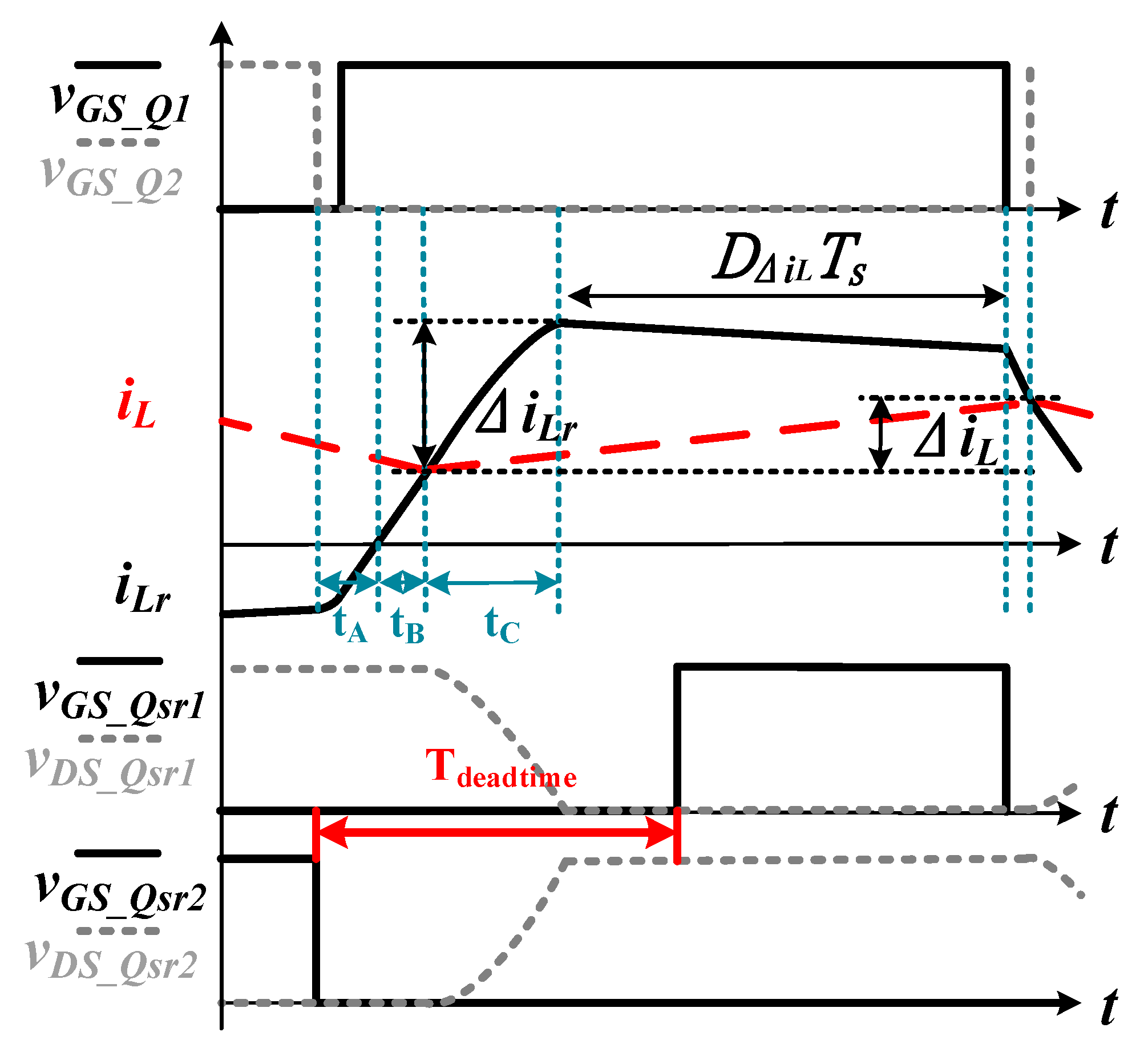
5. Design Considerations
For the main switch to achieve ZVS, the maximum inductance for
Lr is given in Equation (9). However, besides satisfying Equation (9), dead time between switches
Qsr1 and
Qsr2 should also be considered.
Figure 12 is a magnified timing diagram to narrate the switching operation. As seen in the figure, there are three main parts within the dead time zone. They are distinguished according to the value of
iLr. Among them, only
tB is directly affected by the resonant inductor. After determining
tB, the resonant inductor
Lr is designed according to Equation (9).
The resonant capacitance affecting the ZVS of the main switches Qsr1 and Qsr2 includes two parts, CossQsr and CossD; their sum is defined as Cr in previous section. There are two criteria to be considered on design of Cr: the change rate of vDS_Qsr2 and the overshoot ∆iLr.
From Equation (7), the time required for
vDS_Qsr2 to rise from zero to
Vin, defined as
tC in
Figure 12, can be deduced.
tC can be expressed as the following equation:
To keep a suitable voltage stress and elapsed time, we first determine the time required for
tC, which is, say
tC_design.
tC_design is then used to calculate the desired value of
Cr. The design rule of
Cr can be deduced by Equation (13):
The value of
Cr concurrently affects the overshoot of
iLr. The overshoot ∆
iLr is depicted as follows:
Since the overshoot of
iLr must be greater than the ripple of the output inductor current, the voltage
vDS_Qsr2 can be slowly reduced from
Vin to zero volts when the
Qsr1 switch is turned off. Consider the forward bias
VF of the circulating current diode
D1. The minimum value of the ∆
iLr to make sure the end value of
iLr is larger than
iL when Q
1 cuts off in the worst case scenario is:
The
represents the maximum output inductor current ripple of the converter. In the case of the step-down converter, it occurs when duty = 0.5. While
represents the time when the actual resonant inductor current is clamped by the
D1 diode, this time can be approximated as the duty cycle time of the step-down converter. However, too large ∆
iLr will increase the circuit’s unnecessary conduction loss. It is generally recommended that the final design value be close to the minimum value, taking only necessary margins for some component uncertainties. After
Cr is determined,
CossD is obtained by subtracting the parasitic capacitance of
CossQsr from the value of
Cr. As a matter of general design, the value of
CossD requires additional shunt capacitance in addition to the parasitic capacitance of the diode itself. Although the parasitic capacitance of semiconductor devices changes with the voltage across it, the designed value of
Cr is higher than the parasitic capacitance of the diodes and MOSFETs. In other words, the externally paralleled capacitors determine the criteria of ZVS, while the effect from the parasitic capacitances can be ignored. After the
Cr design is completed, the minimum value of
ILr_NP is known from Equation (10), i.e.,
ILr_D1_ON can be obtained. Then
tA can be approximated as:
The overall minimum dead time is tA + tB + tC. The actual dead time must be greater than this minimum value to ensure that the circuit can properly achieve ZVS.
6. Simulation and Experimental Results
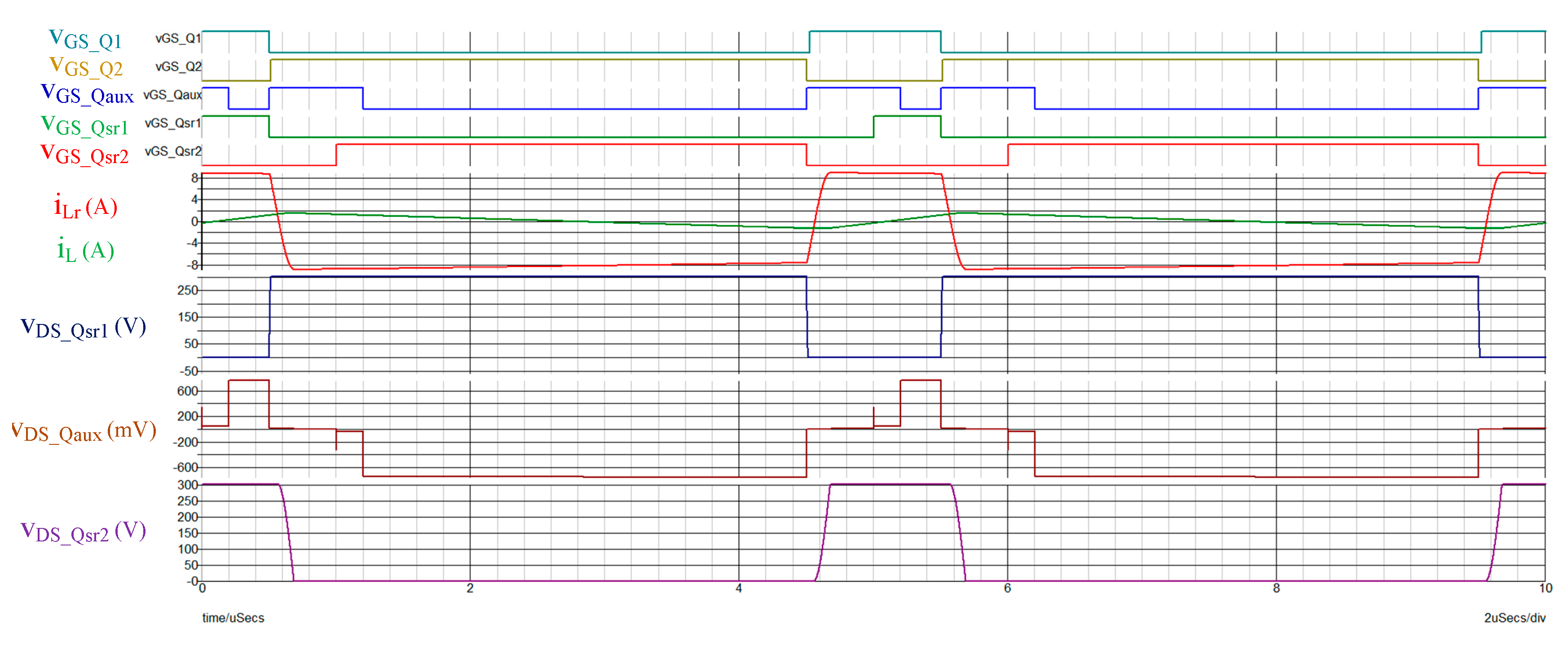
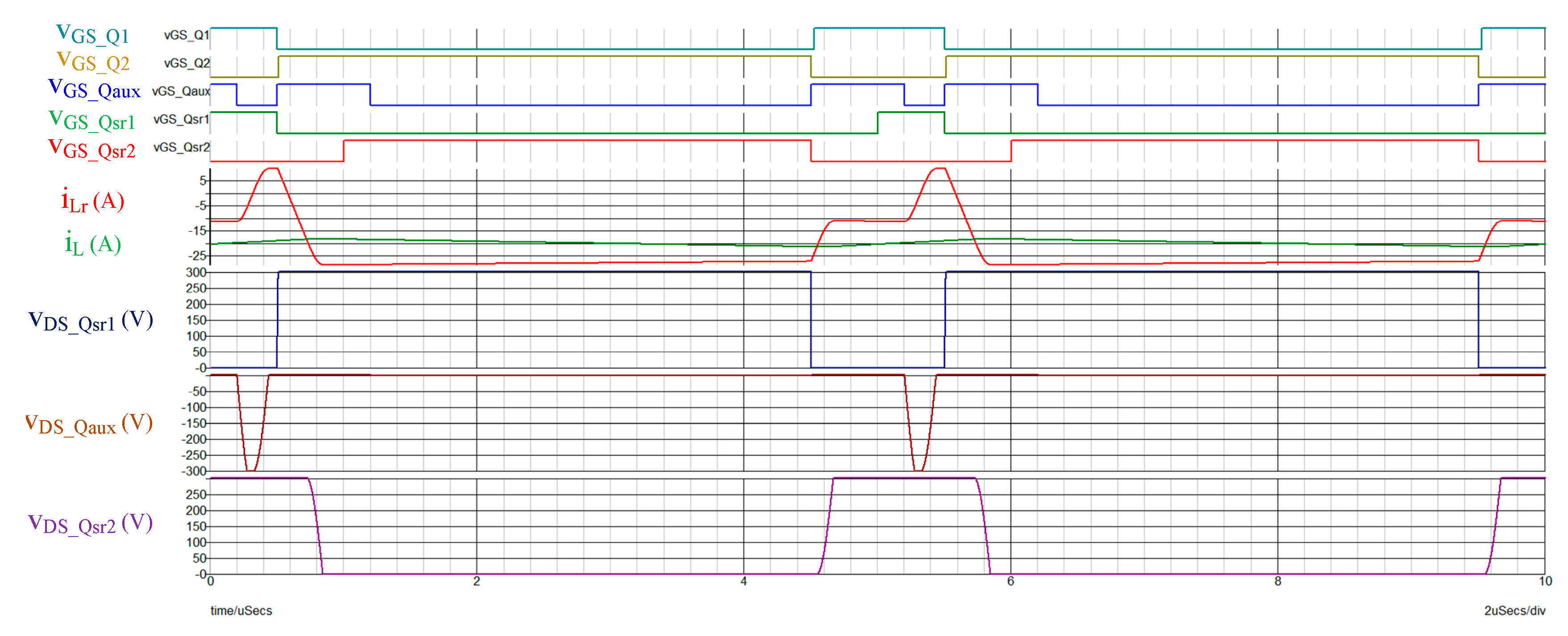
For verification that the topology has the ability to naturally transform the power flow, and the switch
Qsr1/
Qsr2 can achieve bilateral zero voltage switching under any load conditions, the results of the simulation analysis are as follows. The key simulation parameters are listed in
Table 1. The simulation conditions are input voltage = 330 V, output voltage = 50 V, and output current = 20 A to −20 A.
Figure 13,
Figure 14 and
Figure 15 show the simulation results of forwarding output = 20 A, output = 0 A, and reverse output = −20 A. Respectively, it can be seen that under any load conditions, both
Qsr1 and
Qsr2 can achieve bilateral zero-voltage switching and slow down the rate of voltage change. The auxiliary switch
Qaux can also achieve full-range zero voltage switching, and the switches
Q1 and
Q2 can achieve zero voltage switching after a certain load, reducing switching losses.
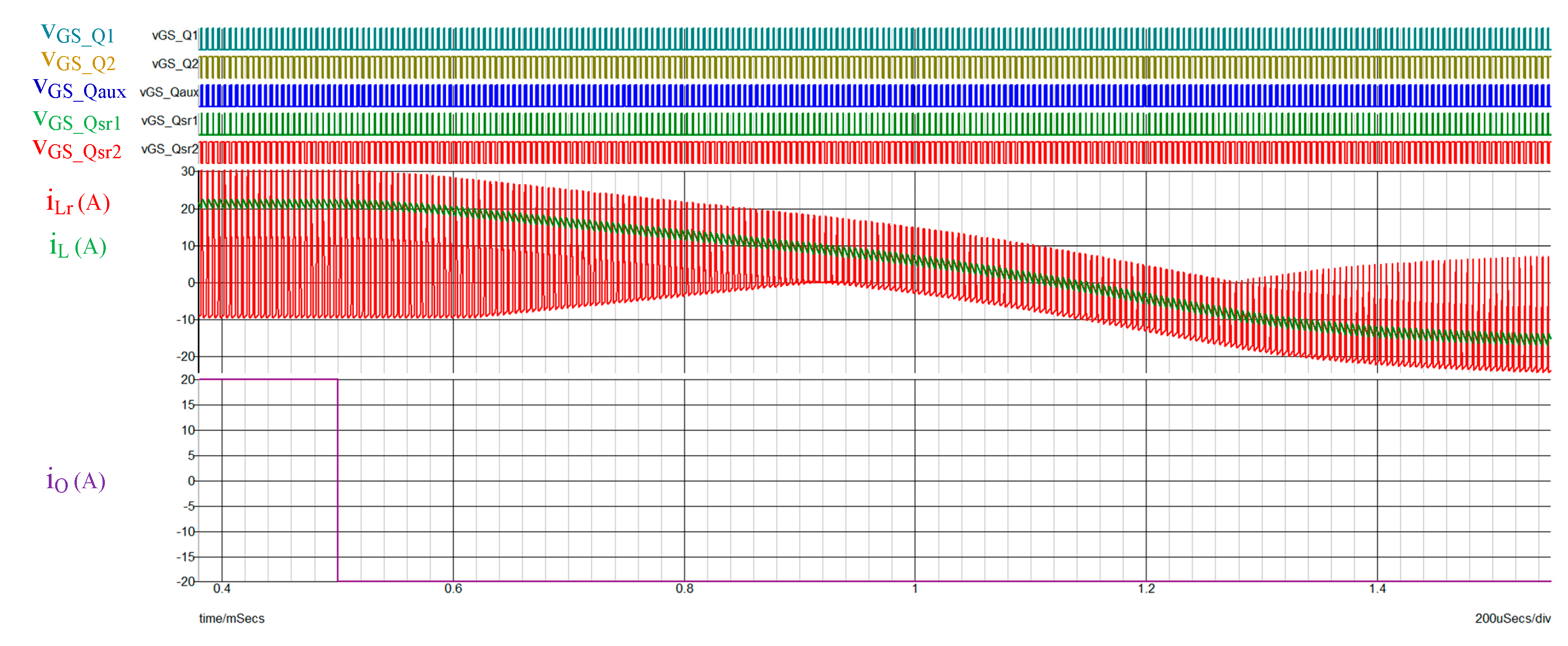
Figure 16 shows the simulation results for an extreme forward-to-reverse conversion. At
t = 0.5 ms, the output current is converted from 20 A to −20 A. The ripple, ∆
iLr, is designed to be 10 A. It can be seen from the figure that the output inductor current
iL follows the behavior of the output current
iO and the current changes from forward to reverse. Under each switching cycle, the resonant inductor current
iLr automatically follows the output inductor current
iL to achieve the
Qsr1 and
Qsr2 bilateral zero voltage switching function. After the zero-voltage switching action, the resonant inductor current
iLr resets to the initial current value cycle by cycle. It can also be seen from the observation of switch signal that the switching signals of the auxiliary switches
Qaux,
Qsr1, and
Qsr2 are the same regardless of the forward or reverse operation. It represents the function of naturally transforming the power flow without adding additional detection circuits and changing different control modes.
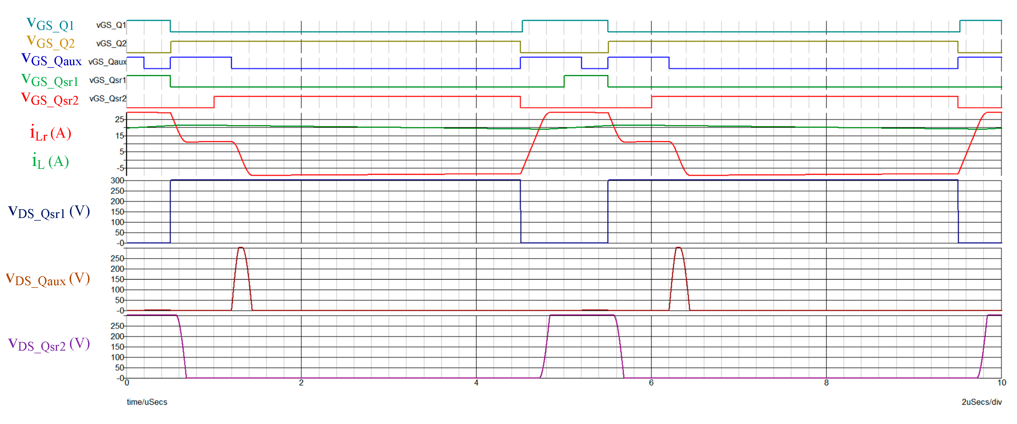
In order to verify the theoretical analysis, a prototype circuit of input voltage Vin = 330 V, output voltage VO = 50–250 V and output power Po = 1 kW is implemented.
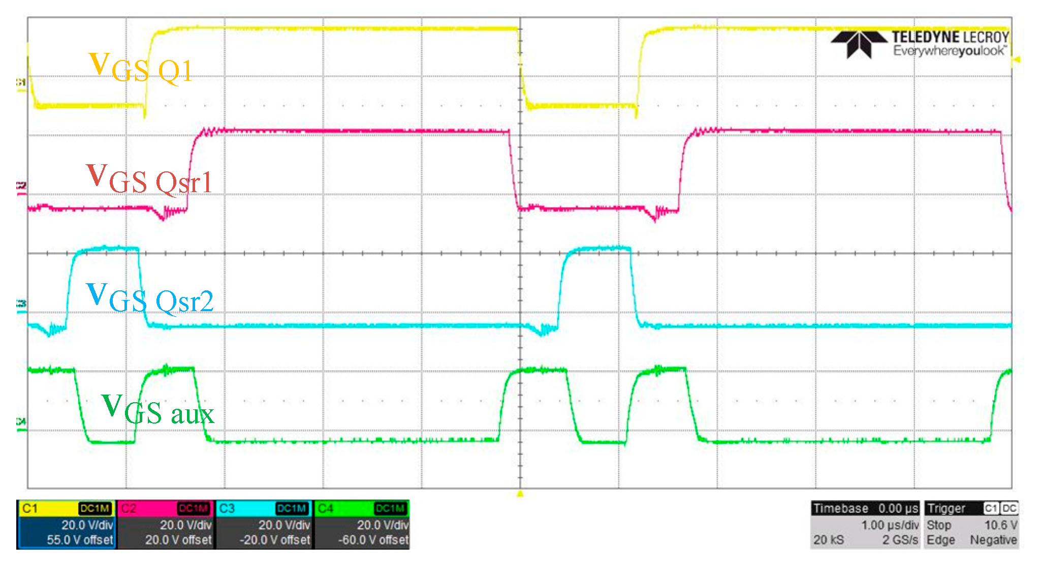
Figure 17 shows the switch’s
vGS signal waveform of
Q1,
Qsr1,
Qsr2 and
Qaux under the test conditions (output voltage = 250 V and output current = 4 A). In addition to verifying the relative position between the switching signals, it can be seen that all
vGS signals have no Miller platform, and it can be seen that all switches have zero voltage switching.
Figure 18 shows the
Qsr1 switch’s
vGS signal,
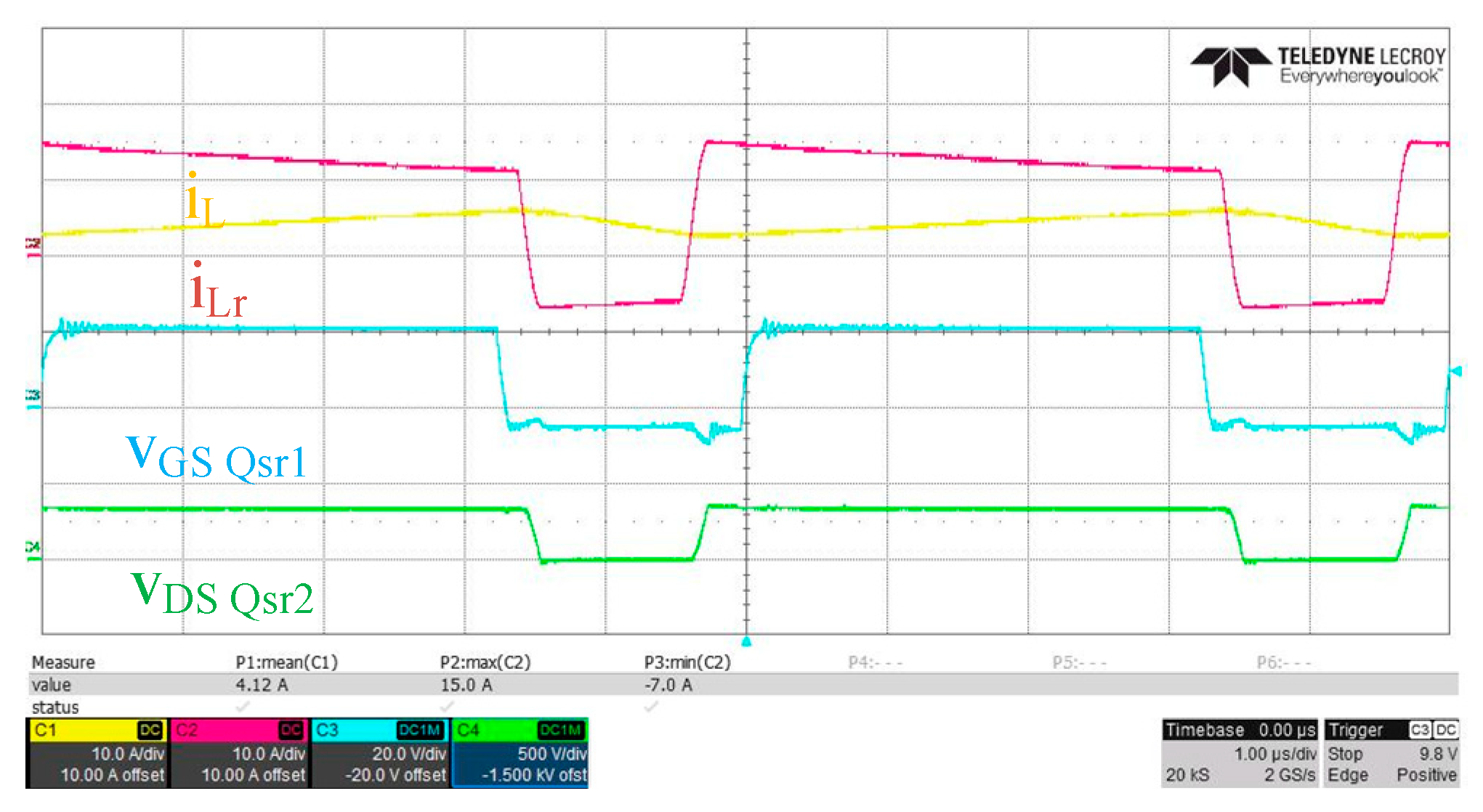
Qsr2 switch’s
vDS voltage, resonant inductor current and output inductor current waveform under the test conditions (output voltage = 50 V and output current = 20 A). The converter operates in continuous current mode. It can be seen that the waveform rise and fall speeds of
vDS_Qsr2 are simultaneously controlled and have the same slope of change.
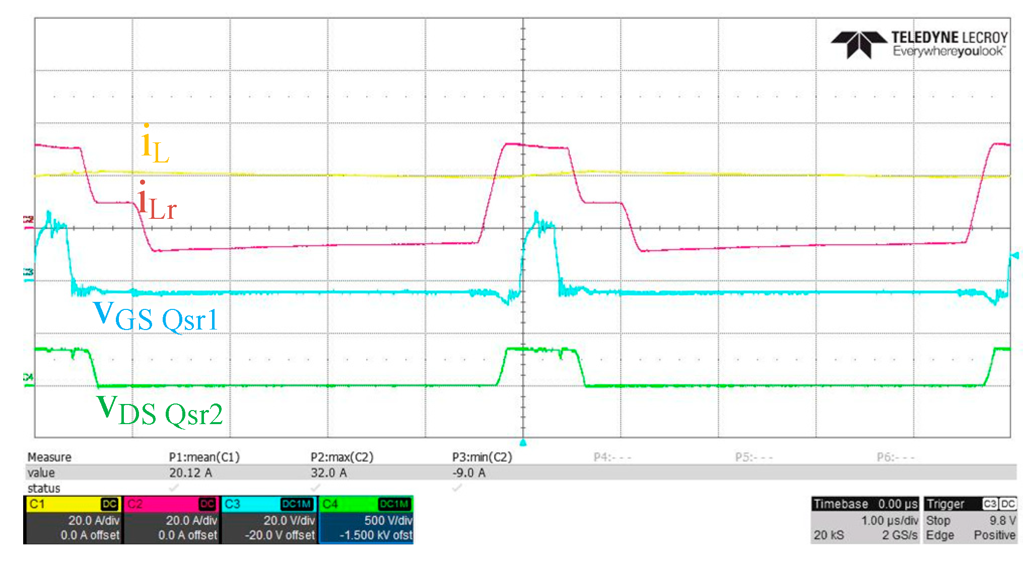
Figure 19 shows the
Qsr1 switch’s
vGS signal,
Qsr2 switch’s
vDS voltage, resonant inductor current and output inductor current waveform under the test conditions (output voltage = 250 V and output current = 4 A). The converter operates in continuous current mode. It can be seen that the waveform rise and fall speeds of
vDS_Qsr2 are simultaneously controlled and have the same slope of change.
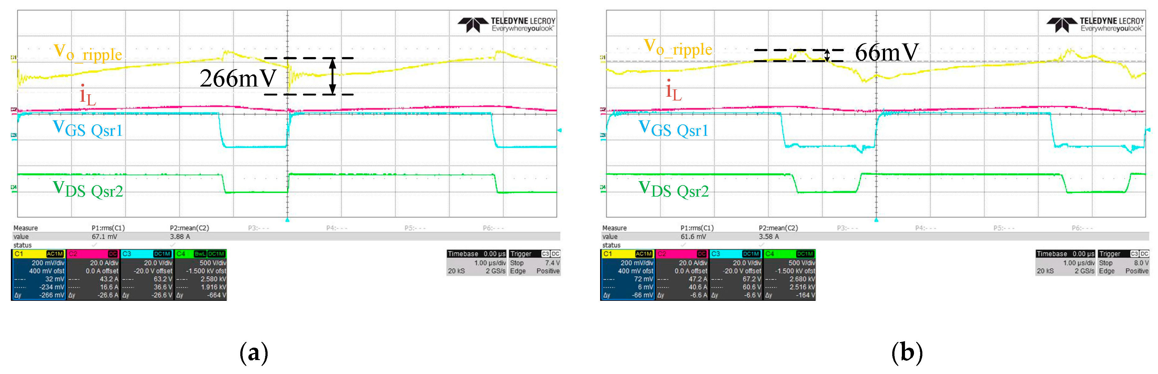
Figure 20a,b show the output voltage ripple with and without the enabling of the auxiliary switching circuit; that is,
Qsr1 is hard/soft switching. Test conditions are output voltage = 250 V and output power = 1 kW. The switching noise observed in
Figure 20a is 266 mV, while it is 66 mV in
Figure 20b. Under the same operation conditions, the output voltage switching noise is greatly reduced by the proposed circuit.
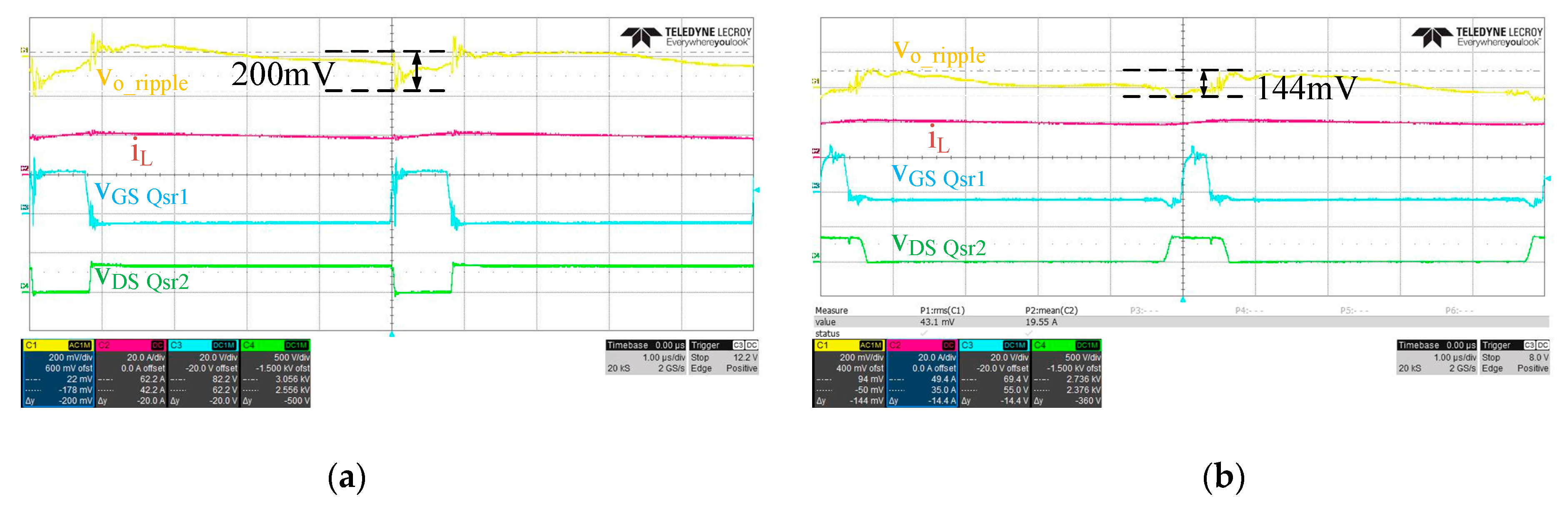
Figure 21a,b represents similar comparisons on switching noise, except that the output voltage = 50 V in this case. The switching noise measured in
Figure 21a is 200 mV, compared to 144 mV in
Figure 21b. Again, switching noise can also be greatly reduced by the proposed scheme. From the experimental results, it is verified that the proposed auxiliary switching circuit can improve the switching noise under adjustable output voltage and current level. This feature is particularly useful for instrument power supplies.


