Abstract
In single phase DC-AC systems, double-line-frequency power ripple appears at the DC side inherently. Normally a large electrolytic capacitor can be used to reduce the power ripple at the DC side. But there are several problems with this method as it decreases the power density and reliability of the converter. In addition, a double-line-frequency current ripple appears in case a voltage source serves at the DC side, which is undesired in specific applications. This paper proposes a single phase DC-AC DAB (dual active bridge) converter with an integrated buck/boost stage for power decoupling purpose under low power condition. The proposed active power decoupling method is able to completely eliminate the double-line-frequency power ripple at the DC side. Therefore, a constant DC current can be obtained for requirements in specific DC-AC applications.
1. Introduction
Proposed in the 1990s, the DAB (dual active bridge) converter attracts much research interests for its high-power-density, isolated and bidirectional power transfer characteristics [1]. It is widely used in various industrial applications such as battery chargers for plug-in hybrid electric vehicles (PHEVs) [2,3], interfaces for renewable energy sources like photovoltaic power systems [4,5,6,7], uninterruptible power supplies (UPS) [8,9] and vehicle-to-grid (V2G) [10,11].
In single phase DC-AC systems, high power ripple appears at the DC side due to the double-line-frequency characteristics of the transmission power at the AC side. In some situations such as photovoltaic applications, more stable transmission power is required to achieve high accuracy of maximum power point tracking (MPPT). If a large electrolytic capacitor is simply used at the DC side, the power density and the reliability of the converter can be decreased significantly and it is not able to completely eliminate the ripple power. If a battery serves at the DC side, the double-line-frequency charging or discharging current would decrease the lifetime of the battery [12,13]. To eliminate the double-line-frequency ripple power at the DC side in single phase power converters, different power decoupling techniques are introduced [14,15]. However, most of the proposed active power decoupling topologies require additional power switches which not only decrease the power density and reliability of the converter, but also bring more cost. The concept of the “parasitic” boost-integrated phase-shift full-bridge converter is proposed in [16]. Two boost-integrated and unidirectional DC-DC topologies, i.e., the symmetric and asymmetric full-bridge converters are presented for specific multi-port applications with one or two integrated boost stages respectively. Compared with the symmetric topology [17], a DC block capacitor in the HF (high frequency) link is indispensable for the asymmetric topology as the average voltage difference between the phase-nodes appears in this case. By adjusting the duty cycles of the legs, bidirectional power flow is realized for the two ports at the primary side of the HF transformer. Similar with the asymmetric topology presented in [16], an active power decoupling method is introduced for CLLC-type resonant DC-AC DAB converter operating in open loop, which is able to effectively realize power decoupling and reduce the capacitance requirement of the converter [18]. In this case, the double-line-frequency ripple power is effectively steered into the passive power decoupling capacitor by adjusting the duty cycle of the modulated leg. Based on this, if the duty cycle of the modulated leg can be appropriately controlled, then the double-line-frequency ripple power can be eliminated due to the mentioned bidirectional power transfer characteristic between the passive energy storage capacitor and the DC source. Therefore, a constant charging or discharging current of the battery can be achieved.
This paper presents the power decoupling of a single phase DC-AC dual active bridge converter based on the integrated bidirectional uni-phase buck/boost stage. The double-line-frequency ripple power is effectively eliminated by the proposed control method on the duty cycle of the bridge leg. The mathematical model of the proposed converter is analyzed in Section 2. The analysis of the control strategy for the proposed converter is presented in Section 3. Simulation and experimental results are illustrated in Section 4. Conclusions are given in Section 5.
2. Mathematical Model of the Converter
The proposed converter is shown in Figure 1. This is a single-stage DC-AC DAB converter with a pseudo intermediate DC link between the synchronous rectifier and the dual active bridges, which is free of the large electrolytic capacitor at the DC link required for the dual-stage DC-AC converter. The AC voltage vg is folded into the voltage vDC1 with a frequency twice that of the AC voltage, which is given by
where Vg is the magnitude of vg and ωg is the angular frequency of vg.
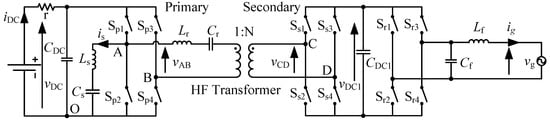
Figure 1.
The proposed DC-AC DAB converter.
The DAB converters are normally controlled by a triple phase shift (TPS) modulation scheme which is shown in Figure 2 [19].
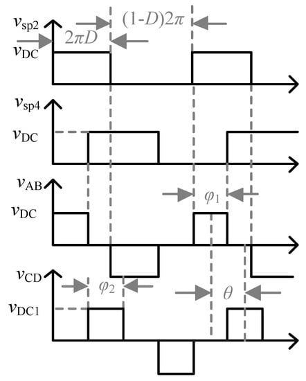
Figure 2.
TPS plus duty cycle modulation scheme.
Two legs in the primary side are phase shifted by φ1 and two legs in the secondary side are phase shifted by φ2. The phase shift angle θ between the voltages vAB and vCD is the third element of this TPS modulation scheme, which determines the direction of the power transfer. In this paper, the duty cycles of the switches on leg A can be regulated, while the duty cycles of other switches are fixed at 50%.
The Fourier-series method is adopted for the mathematical analysis of the converter in this paper. In this approach, the significant harmonics of the circuit waveforms are all taken into account, and the basic AC-circuit theory is used to analyze the resonant converter. The voltage vAO across the switch Sp2 and the voltage vBO across the switch Sp4 with the duty cycle modulation are given by
From (2) and (3), vAB is given by
Also, vCD is given similarly by
This converter can be simplified by using the circuit model as shown in Figure 3.
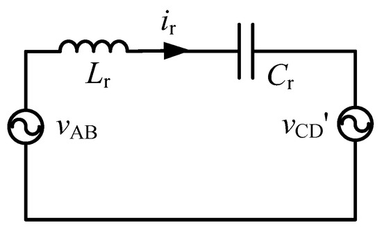
Figure 3.
Simplified circuit model of the converter.
The nth harmonic component of ir is given by
where N is the turns ratio of the HF transformer, and are the phasors of the nth harmonic component of and . and are given by
The nth harmonic average power component Pan is given by
where and represent the magnitudes of and , and represent the arguments of and .The transmission power of the converter is given by
By substituting relevant parameters of the converter, the denominator of (10), namely , increases rapidly with higher harmonics. Its value is 1.27, 58.18, 278.26 and 770.26 for fundamental, third, fifth and seventh harmonics respectively. Thus only the fundamental transmission power of the converter will be considered to calculate the transmission power as shown in (11)
where the reactance X1 of the resonant tank at fundamental frequency is given by
If D is ideally near 1/2, then (11) can be simplified as
From (13) it is evident that the phase shift angle θ between the voltages vAB and vCD determines the direction of the power transfer. When vAB leads vCD by the phase shift angle θ, the power transfers from the DC side to the AC side. When vAB lags vCD by θ, then the power transfers from the AC side to the DC side. The bidirectional power transfer feature of the DAB converters is thus realized through the control of the phase shift angle θ. The average power transferred to the AC side is given by
Then the magnitude of ig is given by
According to (13), if and are fixed, then should be regulated as in order to achieve unity power factor at the AC side [20,21,22], which is shown in Figure 4. Tg represents the AC voltage period. This modulation method for φ2 ensures the balance between the transmission power of the DAB converter and the AC side power, which realizes a pseudo DC link between the DAB converter and the synchronous rectifier free of the large electrolytic capacitor used in the dual-stage converter.
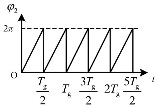
Figure 4.
The modulation scheme of φ2.
According to (11), assuming θ = π/2, two three-dimensional plots of the transmission power characterization with and ( is defined as the maximum deviation magnitude of the duty cycle D) are shown in Figure 5. p is defined as , where is given by
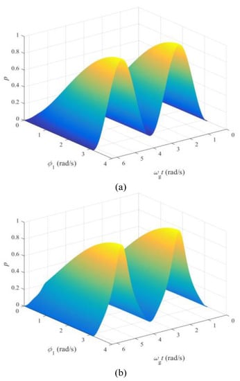
Figure 5.
Three-dimensional plots of the transmission power characterization with duty cycle modulation (a) dmax = 0.05; (b) dmax = 0.35.
The transmission power of the DAB converter fluctuates at 100 Hz frequency and the transmission power increases with bigger phase shift angle φ1. As shown in Figure 5, it is obvious that the transmission power of the DAB converter is near the ideal 100 Hz sinusoidal waveform with dmax = 0.05, and is greatly distorted with higher dmax = 0.35. The distorted transmission power with dmax = 0.35 can cause distortion in the AC side current. Therefore, it is reasonable to use the simplified (13) if a small dmax value can be obtained.
3. Control Strategy
The integrated buck/boost stage at the primary side of the HF transformer for power decoupling is shown in Figure 6. Cs, Ls, two switches of the leg A and the DC bus form a bidirectional Buck/Boost topology inherently, by which the power decoupling is realized. If is > 0, the topology works in Buck mode. If is < 0, then the topology works in Boost mode.
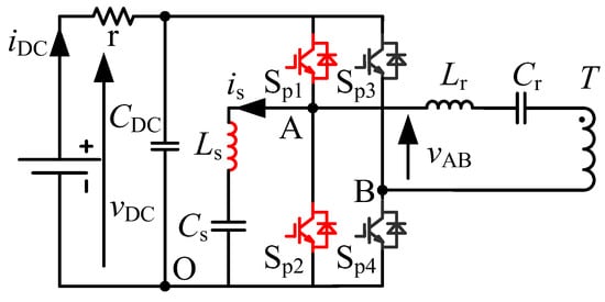
Figure 6.
The integrated buck/boost stage at the primary side of the HF transformer for power decoupling.
The two working modes of the integrated buck/boost stage are illustrated in Figure 7. Ls works as a part of the low-pass filter in the Buck mode, and works as a Boost inductor in the Boost mode.
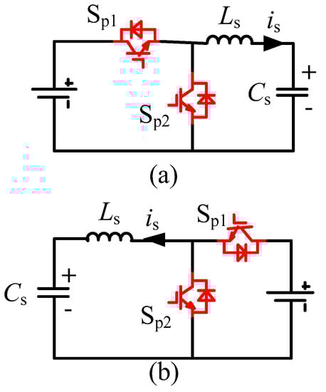
Figure 7.
Two working modes of the integrated buck/boost stage (a) Buck mode with is > 0; (b) Boost mode with is < 0.
Assuming that the AC side voltage and current are in phase, vg and ig are given by
Then the AC side power Pg is given by
It is clear that Pg consists of two components, i.e., the average part and the oscillating part . As the battery serves at the DC side, the DC side power is required to be constant, which equals to the average part of Pg. Therefore, the oscillating power should somehow be mitigated through energy storage buffers.
The ideal power decoupling performance of the integrated buck/boost stage is shown in Figure 8. Pg represents the AC side power, Pavg represents the average power of Pg, iDC0 represents the DC side current without any control, Pc represents the ideal decoupling power transferred into the decoupling capacitor Cs, Ec represents the ideal storage energy of Cs, us represents the voltage of Cs, and is represents the ideal power steering current.
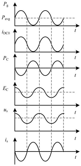
Figure 8.
The ideal power decoupling performance of the integrated buck/boost stage.
As us can be controlled by the duty cycle of the leg A, the ripple power is supposed to be completely eliminated by adjusting the duty cycle properly. The relation between the power decoupling capacitor Cs and the duty cycle deviation d is given in [18] as
where is the maximum deviation magnitude of the modulated duty cycle D.
The overall control diagram is shown in Figure 9. Iavg and iripple represent the average component and the ripple component of iDC respectively. Iavg* and i* represent reference values for Iavg and iripple respectively. The phase shift angle φ2 is as follows: (shown in Figure 4) and the phase shift angle θ is fixed as π/2. To obtain a specific value for the charging or discharging current of the battery, φ1 is used to control Iavg through a proportional-integral (PI) controller (error value IE as input, φ1 as output), thus the battery charging or discharging current can be regulated based on the value of Iavg*. Additionally, iripple is controlled by the proportional resonant (PR) controller [23] (−iripple as input, D as output). The non-ideal PR controller transfer function is given by
where the , , and represent the proportional term, the resonant term gain, the cut-off frequency and the resonant frequency respectively. According to the internal model principle, if a sinusoidal mathematical model included, the controller can realize zero steady-state error following a sinusoidal reference input signal at the specific frequency [24]. The bode diagrams of the non-ideal PR controller are shown in Figure 10, with , , rad/s and rad/s. As shown in Figure 10, a high gain at the resonant frequency is obtained. And the bandwidth can be widened with a higher value of and vice versa. A wider bandwidth is helpful when the frequency variation effect occurs.
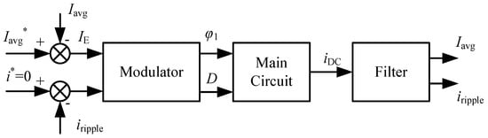
Figure 9.
The overall control diagram for the proposed DC-AC DAB converter with DC side power decoupling.
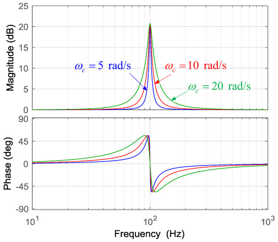
Figure 10.
The bode diagram of the non-ideal PR controller.
The control loop designed to control Iavg is shown in Figure 11. GLPF represents the transfer function of the low-pass filter (LPF). GPI represents the PI controller. Gc represents the transfer function from φ1 to iDC. Iavg* is set as 0.5 A in the following analysis.
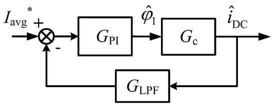
Figure 11.
Control loop for the purpose of Iavg control.
According to (14), assuming that the PR controller is working appropriately and the DC side power ripple is almost eliminated, then iDC can be given by
Gc is given by
GLPF is given by
where the damping coefficient natural angular frequency rad/s. GPI is given as
The loop gain of the system is given by
In the steady state, φ1 is calculated as 1.03 rad/s according to (21) assuming that iDC is ideally controlled as Iavg*. Then the bode diagram of the corrected open-loop transfer function is shown in Figure 12. As shown in this figure, the phase margin is enough to meet the stability requirement of the system.
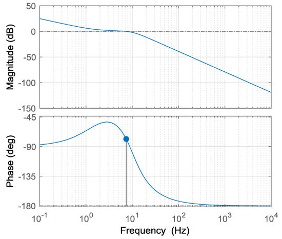
Figure 12.
The bode diagram of the corrected open-loop transfer function for Iavg control.
4. Simulation and Experimental Results
The simulation and experimental results of the proposed DC-AC DAB converter with DC side power decoupling under low power condition are shown in this section.
4.1. Simulation Results
The main parameters of the MATLAB Simulink model are given in Table 1.

Table 1.
Parameters of the MATLAB Simulink model.
With φ1 = π/2, θ = π/2, the simulation results of the AC side voltage vg and current ig, DC side current iDC without the DC side power decoupling are shown in Figure 13. From Figure 13c, there is a 100 Hz ripple current, or a 100 Hz ripple power at the DC side because of the double-line-frequency power transmission nature at the AC side. It is noted that the unity power factor is achieved at the AC side due to the applied modulation scheme for the phase shift angle φ2.
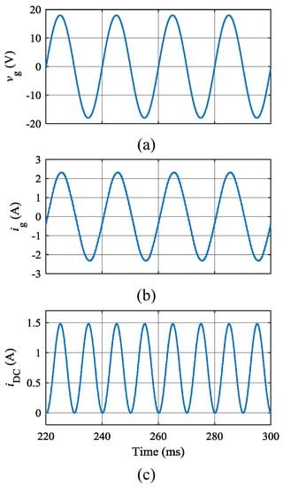
Figure 13.
With φ1 = π/2, θ = π/2, (a) the AC side voltage vg; (b) AC side current ig; and (c) DC side current iDC without the DC side power decoupling.
With φ1 = π/2, θ = π/2, the simulation results of ig, iDC, the power decoupling capacitor Cs voltage us and current is with the DC side power decoupling are shown in Figure 14. According to (20), the parameters of the PR controller are as follows: , , rad/s and rad/s.
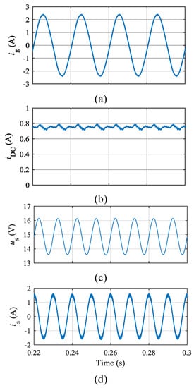
Figure 14.
With φ1 = π/2, θ = π/2, (a) ig; (b) iDC; (c) the power decoupling capacitor Cs voltage us; and (d) the power decoupling capacitor Cs current is.
From Figure 14b, the 100 Hz ripple power at the DC side is almost eliminated, thus a relatively stable DC side current is obtained, which is important when the DC source is a battery. From Figure 14c,d, as the duty cycle of leg A is modulated, the power decoupling capacitor Cs voltage us fluctuates at 100 Hz frequency and balances the 100 Hz ripple power at the DC side. Also, the fluctuation range of us is relatively small, thus the modulation range of the duty cycle is small, which will not cause a distortion in the transmission power and the AC side current ig as shown in Figure 14a.
The simulation results of the voltages vAB, vCD, and the transformer primary side current ir are shown in Figure 15. As φ1 is set as π/2, the width of the positive part and the negative part of vAB is π/2, and vAB leads vCD by θ = π/2. The envelope of the transformer secondary voltage vCD under this condition is shown in Figure 16. According to vCD1 given in (1), the magnitude of vCD has a 100 Hz envelope.
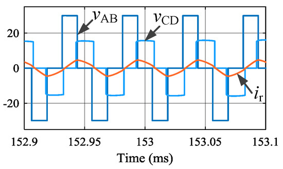
Figure 15.
vAB, vCD and the transformer primary side current ir (φ1 = π/2, θ = π/2).
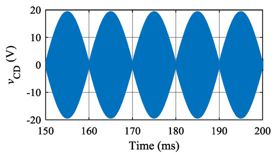
Figure 16.
The envelope of the transformer secondary voltage vCD (φ1 = π/2, θ = π/2).
Assuming the battery charging or discharging current is required as Iavg* = 1 A, by adding the Iavg control loop shown in Figure 9, iDC and φ1 are shown in Figure 17. It is clear that iDC is controlled at the desired constant value 1 A.
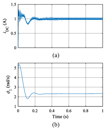
Figure 17.
(a) iDC and (b) φ1 with the Iavg control loop (Iavg* = 1 A).
4.2. Experimental Results
The experimental settings are shown in Figure 18. The parameters of the experimental settings are the same as the simulation parameters shown in Table 1. With φ1 = π/2, θ = π/2, the experimental results of the AC side voltage vg and current ig, DC side current iDC without the DC side power decoupling are shown in Figure 19. Similar with the simulation results shown in Figure 13, there appears a 100 Hz ripple current, or a 100 Hz ripple power at the DC side because of the double-line-frequency power transmission nature at the AC side.
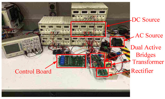
Figure 18.
The experimental settings.
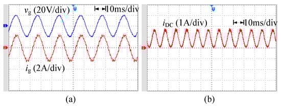
Figure 19.
With φ1 = π/2, θ = π/2, experimental results of (a) the AC side voltage vg and current ig; (b) DC side current iDC without the DC side power decoupling.
With φ1 = π/2, θ = π/2, the experimental results of the AC side voltage vg and current ig, DC side current iDC with the DC side power decoupling are shown in Figure 20. The power decoupling capacitor Cs voltage us and current is are shown in Figure 21.
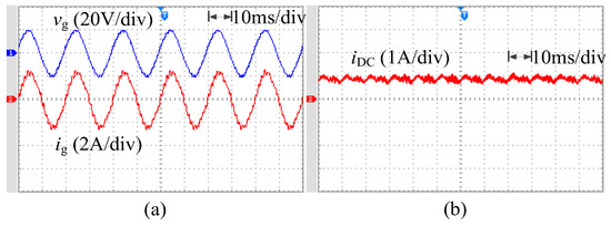
Figure 20.
With φ1 = π/2, θ = π/2, experimental results of (a) vg and ig; (b) iDC with the DC side power decoupling.
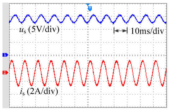
Figure 21.
The power decoupling capacitor Cs voltage us and current is.
Comparing Figure 20a with Figure 14a, and Figure 20b with Figure 14b, it is obvious that the experimental results verify the simulation results. The experimental result of iDC is about 0.91 A, which is near the simulation result of iDC. The 100 Hz ripple power at the DC side is almost eliminated compared with Figure 19b, thus a more stable DC side current is obtained. Compared with Figure 14c, the average value of us in Figure 21 is a bit lower than the expected value due to the voltage drop at the DC side in the experimental test. With the duty cycle modulation, the power decoupling capacitor Cs voltage us fluctuates at 100 Hz frequency and thus the 100 Hz ripple power at the DC side is eliminated.
The experimental result of the transformer secondary voltage vCD in this condition is shown in Figure 22. According to vDC1 given in (1), vCD shows a 100 Hz envelope with a magnitude of 18 V (Vg).
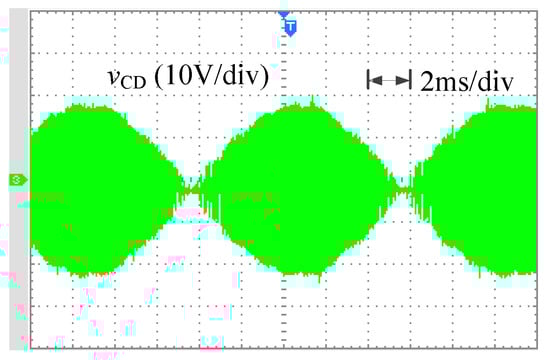
Figure 22.
The experimental result of the transformer secondary voltage vCD (φ1 = π/2, θ = π/2).
The experimental results of iDC with the PR control plus Iavg control loop (Iavg* = 1 A) are shown in Figure 23. In this condition, φ1 is controlled as 1.62 rad/s compared with the simulation result of 2.2 rad/s shown in Figure 17b. It is noted that iDC is controlled as Iavg* = 1 A.
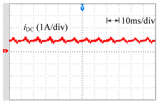
Figure 23.
The DC side current iDC with PR control plus Iavg control loop (Iavg* = 1 A).
5. Conclusions
The basic characteristics of the single stage DC-AC DAB converter with an integrated uni-phase buck/boost stage for DC side power decoupling purpose under low power condition is analyzed in detail based on the mathematical analysis, simulations and experiments. Not only the power density and reliability of the converter is enhanced as no additional power switch is added, but also the cost of the converter is decreased. By controlling the duty cycle of the specific leg, the integrated uni-phase buck/boost stage is able to completely eliminate the double-line-frequency ripple power with PR control, which is verified in the simulation and experimental results. In addition, a current loop is added to obtain a specific constant value for the charging or discharging current of the DC source.
Author Contributions
J.H. did the simulations, experiments and wrote the manuscript; M.V. offered the research idea, supervision and guidance; J.Y. supported and guided the succeeding research, and offered revision and proofreading; Y.L., J.P., and H.J. offered guidance, and proofreading.
Funding
This research was funded by National Natural Science Foundation of China (No. 51707124, No. 51477104), Department of Education of Guangdong Province (No. 2016KQNCX148), Natural Science Foundation of Guangdong Province (No. 2016A030313041), Shenzhen Science and Technology Research Foundation for Basic Project (No. JCYJ20170302153607971), and Shenzhen Peacock Program (No. 827-000237).
Conflicts of Interest
The authors declare no conflict of interest.
References
- De Doncker, R.W.; Divan, D.M.; Kheraluwala, M.H. A three-phase soft-switched high-power-density DC/DC converter for high-power applications. IEEE Trans. Ind. Appl. 1993, 27, 63–73. [Google Scholar] [CrossRef]
- Xue, L.; Shen, Z.; Boroyevich, D.; Mattavelli, P.; Diaz, D. Dual Active Bridge-Based Battery Charger for Plug-in Hybrid Electric Vehicle With Charging Current Containing Low Frequency Ripple. IEEE Trans. Power Electron. 2015, 30, 7299–7307. [Google Scholar] [CrossRef]
- Wang, Y.-C.; Ni, F.-M.; Lee, T.-L. Hybrid Modulation of Bidirectional Three-Phase Dual-Active-Bridge DC Converters for Electric Vehicles. Energies 2016, 9, 492. [Google Scholar] [CrossRef]
- Wang, W.; Ruan, X.; Wang, X. A novel second harmonic current reduction method for dual active bridge used in photovoltaic power system. In Proceedings of the IEEE Energy Conversion Congress and Exposition, Denver, CO, USA, 15–19 September 2013. [Google Scholar]
- Sathishkumar, P.; Himanshu; Piao, S.; Khan, M.A.; Kim, D.-H.; Kim, M.-S.; Jeong, D.-K.; Lee, C.; Kim, H.-J. A Blended SPS-ESPS Control DAB-IBDC Converter for a Standalone Solar Power System. Energies 2017, 10, 1431. [Google Scholar] [CrossRef]
- Vavilapalli, S.; Padmanaban, S.; Subramaniam, U.; Mihet-Popa, L. Power Balancing Control for Grid Energy Storage System in Photovoltaic Applications—Real Time Digital Simulation Implementation. Energies 2017, 10, 928. [Google Scholar] [CrossRef]
- Duman, T.; Marti, S.; Moonem, M.A.; Abdul Kader, A.A.R.; Krishnaswami, H. A Modular Multilevel Converter with Power Mismatch Control for Grid-Connected Photovoltaic Systems. Energies 2017, 10, 698. [Google Scholar] [CrossRef]
- Bekiarov, S.B.; Emadi, A. Uninterruptible power supplies: Classification, operation, dynamics, and control. In Proceedings of the IEEE Applied Power Electronics Conference and Exposition, Dallas, TX, USA, 10–14 March 2002. [Google Scholar]
- Jeong, D.K.; Ryu, M.H.; Kim, H.G.; Kim, H.J. Optimized Design of Bi-Directional Dual Active Bridge Converter for Low-Voltage Battery Charger. J. Power Electron. 2014, 14, 468–477. [Google Scholar] [CrossRef]
- Sha, D.; Xu, G.; Xu, Y. Utility Direct Interfaced Charger/Discharger Employing Unified Voltage Balance Control for Cascaded H-Bridge Units and Decentralized Control for CF-DAB Modules. IEEE Trans. Ind. Electron. 2017, 64, 7831–7841. [Google Scholar] [CrossRef]
- Lopes, J.A.P.; Soares, F.J.; Almeida, P.M.R. Integration of Electric Vehicles in the Electric Power System. Proc. IEEE 2011, 99, 168–183. [Google Scholar] [CrossRef]
- Fontes, G.; Turpin, C.; Astier, S.; Meynard, T.A. Interactions between Fuel Cells and Power Converters: Influence of Current Harmonics on a Fuel Cell Stack. IEEE Trans. Power Electron. 2007, 22, 670–678. [Google Scholar] [CrossRef]
- Shimizu, T.; Jin, Y.; Kimura, G. DC ripple current reduction on a single-phase PWM voltage-source rectifier. IEEE Trans. Ind. Appl. 2000, 36, 1419–1429. [Google Scholar] [CrossRef]
- Tang, Y.; Blaabjerg, F. Power decoupling techniques for single-phase power electronics systems—An overview. In Proceedings of the IEEE Energy Conversion Congress and Exposition, Montreal, QC, Canada, 20–24 September 2015. [Google Scholar]
- Qin, Z.; Tang, Y.; Loh, P.C.; Blaabjerg, F. Benchmark of AC and DC Active Power Decoupling Circuits for Second-Order Harmonic Mitigation in Kilowatt-Scale Single-Phase Inverters. IEEE J. Emerg. Sel. Top. Power Electron. 2016, 4, 15–25. [Google Scholar] [CrossRef]
- Al-Atrash, H.; Batarseh, I. Boost-Integrated Phase-Shift Full-Bridge Converter for Three-Port Interface. In Proceedings of the IEEE Power Electronics Specialists Conference, Orlando, FL, USA, 17–21 June 2007. [Google Scholar]
- Li, W.; Xiao, J.; Zhao, Y.; He, X. PWM Plus Phase Angle Shift (PPAS) Control Scheme for Combined Multiport DC/DC Converters. IEEE Trans. Power Electron. 2012, 27, 1479–1489. [Google Scholar] [CrossRef]
- Malan, W.L.; Vilthgamuwa, D.M.; Walker, G.R.; Broadmeadow, M.A.H.; Thrimawithana, D.; Madawala, U. A single phase AC–DC bidirectional converter with integrated ripple steering. In Proceedings of the IEEE 8th International Power Electronics and Motion Control Conference (IPEMC-ECCE Asia), Hefei, China, 22–26 May 2016. [Google Scholar]
- Zhao, B.; Song, Q.; Liu, W.; Sun, Y. Overview of Dual-Active-Bridge Isolated Bidirectional DC–DC Converter for High-Frequency-Link Power-Conversion System. IEEE Trans. Power Electron. 2014, 29, 4091–4106. [Google Scholar] [CrossRef]
- Weerasinghe, D.S.B.; Madawala, U.K.; Thrimawithana, D.J.; Vilathgamuwa, D.M. A technique for improving grid side harmonic distortion of matrix converter based bi-directional IPT systems. In Proceedings of the 39th Annual Conference of the IEEE Industrial Electronics Society (IECON), Vienna, Austria, 10–13 November 2013. [Google Scholar]
- Weerasinghe, S.; Madawala, U.K.; Thrimawithana, D.J. A Matrix Converter-Based Bidirectional Contactless Grid Interface. IEEE Trans. Power Electron. 2017, 32, 1755–1766. [Google Scholar] [CrossRef]
- Weerasinghe, S.; Thrimawithana, D.J.; Madawala, U.K. Modeling Bidirectional Contactless Grid Interfaces with a Soft DC-Link. IEEE Trans. Power Electron. 2015, 30, 3528–3541. [Google Scholar] [CrossRef]
- Teodorescu, R.; Blaabjerg, F.; Liserre, M.; Loh, P.C. Proportional-resonant controllers and filters for grid-connected voltage-source converters. IEEE Proc. Electric Power Appl. 2006, 153, 750–762. [Google Scholar] [CrossRef]
- Fukuda, S.; Yoda, T. A novel current-tracking method for active filters based on a sinusoidal internal model [for PWM invertors]. IEEE Trans. Ind. Appl. 2001, 37, 888–895. [Google Scholar] [CrossRef]
© 2018 by the authors. Licensee MDPI, Basel, Switzerland. This article is an open access article distributed under the terms and conditions of the Creative Commons Attribution (CC BY) license (http://creativecommons.org/licenses/by/4.0/).