Article

X-ray Diffraction, Micro-Raman and X-ray Photoemission Spectroscopic Investigations for Hydrothermally Obtained Hybrid Compounds of Delafossite CuGaO2 and Wurtzite ZnO

1
Field of Advanced Ceramics, Department of Life Science and Applied Chemistry, Nagoya Institute of Technology, Gokiso, Showa, Nagoya 466-8555, Japan
2
Department of Materials Science and Engineering, University of Erlangen-Nuremberg, Martensstraße 7, DE-91058 Erlangen, Germany
3
Frontier Research Institute of Materials Science (FRIMS), Nagoya Institute of Technology, Gokiso, Showa, Nagoya 466-8555, Japan
*
Author to whom correspondence should be addressed.
Ceramics 2022, 5(4), 655-672; https://doi.org/10.3390/ceramics5040048
Submission received: 30 August 2022 / Revised: 10 September 2022 / Accepted: 14 September 2022 / Published: 22 September 2022
(This article belongs to the Special Issue Advances in Ceramics)

Abstract

:
P-type delafossite CuGaO2 is a wide-bandgap semiconductor for optoelectronic applications, and its lattice parameters are very similar to those of n-type semiconductor wurtzite ZnO. Accordingly, the investigation of crystalline heterostructures of CuGaO2 and ZnO has attracted significant attention. In this study, interfacial CuGaO2/ZnO hetero-compounds were examined through X-ray diffraction (XRD) analysis, confocal micro-Raman spectroscopy, and X-ray photo-electron spectroscopy (XPS). XRD and Raman analysis revealed that the hydrothermal deposition of ZnO on hexagonal platelet CuGaO2 base crystals was successful, and the subsequent reduction process could induce a unique, unprecedented reaction between CuGaO2 and ZnO, depending on the deposition parameters. XPS allowed the comparison of the binding energies (peak position and width) of the core level electrons of the constituents (Cu, Ga, Zn, and O) of the pristine CuGaO2 single crystallites and interfacial CuGaO2/ZnO hybrids. The presences of Cu2+ ions and strained GaO6 octahedra were the main characteristics of the CuGaO2/ZnO hybrid interface. The XPS and modified Auger parameter analysis gave an insight into a specific polarization of the interface, promising for further development of CuGaO2/ZnO hybrids.

1. Introduction

The development of semiconducting materials that can produce hydrogen [1], decompose organic pollutants [2], and improve power generation efficiency [3] toward environmental purification and energy management is a growing research field that has received significant attention from material chemists as well as device manufacturers [4,5]. Copper-based delafossite oxides with a composition of CuMO2 (M = Al, Ga, Cr) have been studied as new p-type semiconductors because of their high hole mobility, nontoxicity, high abundance, environmental friendliness, and low cost [6].
Delafossite-type copper gallate (CuGaO2) has a rhombohedral (3R) or hexagonal (2H) symmetry, with a layer of distorted GaO6 octahedra which were sandwiched between linear O–Cu–O chains parallel to c-axis [7]. The valence band is composed of an electronic hybrid of the 3d orbital of Cu atoms and the 2p orbital of O atoms, which is delocalized by oxygen atoms and forms at a low energy level. In addition, Cu vacancies and interstitial O atoms can produce holes, resulting in p-type conductivity [8]. As a wide-band-gap semiconductor, CuGaO2 possesses a direct band gap at high energy of 3.4–3.7 eV and a small absorption tail starting at 2 eV due to an indirect band gap [9], which enables its applications in p-n junction devices, p-type dye-sensitized solar cells, and photocatalysts [10,11,12]. Ehara [13] successfully fabricated transparent delafossite-type CuGaO2 thin films for dye-sensitized solar cells by a sol-gel method. The Ga source materials were dissolved in nitrate or acetylacetonate sols, and the films prepared with acetylacetonate had a higher transmittance than those prepared with nitrate. Xu et al. [14] reported the formation of ZnO nanowires with n-type semiconductor properties on the surface of p-type delafossite, CuGaO2. The multihorned composites of hexagonal platelet CuGaO2 in 3R structure and ZnO nanowires were successfully fabricated by a hydrothermal method. The luminescence from ZnO nanowires and electron-hole recombination at the p-n junction interface were observed in the composites.
Figure 1 shows the crystal structures of delafossite 3R CuGaO2 and wurtzite ZnO; their lattice parameters (a, b, c, α, β, and γ) can be compared. Despite their different crystal structures, as shown in Figure 1a,b, the lattice parameters of the rhombohedral CuGaO2 structure (R-3m) [7] are very similar to those of the hexagonal ZnO (P63mc) [15], as shown in Figure 1c,d. Particularly, Cu (or O) in the c plane [(006) plane] is stacked to form triangles with a side length of 2.9770(8) Å in delafossite CuGaO2, whereas Zn (or O) forms triangles with a side length of 3.25010(1) Å, as indicated by the yellow dashed line. Hexagons with side lengths of 1.7188 Å in CuGaO2 and 1.8764 Å in ZnO structures [red line in Figure 1c] suggest the possibility to form CuGaO2/ZnO (CGO/ZnO) heterostructure. Figure 2 shows a prospected electronic structure of p-n heterostructure as a model of CuGaO2(p-type)-ZnO(n-type) hybrids. It is well known that in a hybrid p-n junction with different types of semiconductors having opposite carrier transport characteristics, band bending of the electronic structure occurs at the interface between the semiconductors [16]. In an n-type semiconductor, as shown in Figure 2i, electrons excited in the conduction band enter the semiconductor because of the potential slope generated by band bending, and the holes in the valence band move to the adjacent semiconductor interface. In contrast, photogenerated holes in the p-type semiconductor remain in the interior, whereas electrons move toward the interface and arrive at the adjacent semiconductor (see Figure 2ii). The continuous excitation of electron-hole pairs is possible at the interface; consequently, electrons and holes experience effective charge separation by the steep slope of the band potential [17,18]. In this case, a redox reaction is expected on each surface (involving electrons and holes on the n- and p-type sides, respectively) when semiconductor heterostructures act as catalysts under light illumination above the band-gap energy (see Figure 2iii).
Whereas the apparent similarity of crystal structures of CuGaO2 and ZnO would promise development of their hybrids, the formation of the p-n junction between CuGaO2 and ZnO is not necessarily obvious because there are no atoms within the distance of 1.7188 (1.8764) Å of Cu (Zn) in the c-plane [see Figure S1a,b in the Electronic Supplementary Information (ESI)]. Moreover, the lattice mismatch of ~10% is quite large, so massively strained growth with a large transition regime between CuGaO2 and ZnO can be anticipated. Thus, further investigation is needed.
Raman spectroscopy is an effective tool for nondestructive characterization of lattice dynamics for various materials and can be used to obtain information on the crystal structures, lattice defects, and phase transitions via the changes in lattice vibration [19]. For example, the half-width of a Raman peak is associated with the crystallinity [20]; a shift in the peak position indicates the strain in the crystal lattice [21], and the covalency of bonds [22], and the intensity of the peak reflects the physical properties such as the concentrations of components [23]. Cu-based delafossite materials are being actively studied by Raman techniques [24,25], and many discussions arise from them. For example, impurity phases undetectable by X-ray techniques, such as CuO [26] and Cu2O [27], were observed, and the identification of many Raman signals that could not be assigned to those of the ideal CuGaO2 structure [28] was suggested in Raman spectra of CuGaO2 crystals.
To characterize the heterostructures, X-ray photoelectron (XP) spectroscopy (XPS) may provide insights into the chemical changes in the constituents of materials. Because XPS uses X-rays as an excitation source, the excitation light does not damage the substances and thus XPS can be used to measure various materials such as polymers, metallic materials, and insulators. X-rays from Mg Kα and Al Kα sources are often used to irradiate materials. They supplement the photoelectrons emitted by the ionization of the materials so that energy analysis can be performed. When one element bonds with another, the intra-atomic electronic state changes, and the binding energy of the core level (CL) also changes; thus, an XP peak shift can be observed. These changes are regarded as chemical shifts and are the most important features of the XP spectra, as they enable state analysis. Gao et al. [29] recently investigated Ca-doped CuScO2 through XPS and reported a possible charge balance in the CuScO2 films owing to the formation of copper vacancy defects after Ca doping. A delafossite thin film on a polymethyl methacrylate or SiO2/Si substrate was also studied via XPS and its electrical and optical properties have been reported [30,31]. In addition to the above-mentioned basic research, recent works expanded the application scope of delafossite materials and heterojunctions. Especially, “self-powered solar-blind photodetectors” are one of the promising devices owing to the increasing demand for energy saving, miniaturization, and high efficiency [32,33,34].
In our previous work [9], the hydrothermal synthesis of a hexagonal platelet crystal of CuGaO2 with a delafossite structure was reported, and it was demonstrated that the particle size of CuGaO2 could be controlled by adding polyethylene glycol (PEG) with different molecular weights (MW = 6000 and 20,000). The photocatalytic activity of CuGaO2/ZnO hybrids with a particle size of approximately 8 μm has been reported. The results showed that the hybrids had better photocatalytic properties than CuGaO2 or ZnO alone, where efficient electron-hole separation in the heterojunction with a ZnO layer on the c plane of the delafossite crystal was suggested as a driving force for the catalytic activity. In this study, XRD and confocal micro-Raman spectra of CuGaO2 platelet crystals and CuGaO2/ZnO hybrids were measured to determine their structures and especially for micro-Raman revealed the vibrational properties of the targeted particle within several μm laser spot size. The changes in the valence states and binding energies of the synthesized CuGaO2 and CuGaO2/ZnO hybrids were also examined by the XPS.

2. Materials and Method

2.1. Preparation of CuGaO2 Powder

The following reagents were used in the hydrothermal synthesis of delafossite CuGaO2: Cu(NO3)2·2.5H2O (Sigma-Aldrich, St. Louis, MO, USA; 99%+), Ga(NO3)2·8H2O (Nacalai Tesque Co., Kyoto, Japan), ethylene glycol (EG) (Kishida Chem. Co., Osaka, Japan), PEG 6000 (MW = 6000) (Kishida Chem. Co.), PEG 20,000 (MW = 20,000) (Kishida Chem. Co.), and KOH (Kishida Chem. Co.). Two samples of CuGaO2 were synthesized using PEG 6000 and PEG 20,000, and the pH of the precursor solution was adjusted accordingly.
The synthesis method has been described in detail elsewhere [9]. Briefly, Cu(NO3)2·2.5H2O (1 mmol) and Ga(NO3)2·8H2O (1 mmol) were dissolved together in 3.6 mL of deionized water. Next, 3 mL EG and 0.1 g of PEG 6000 or PEG 20,000 were added. KOHaq (5 mmol) was introduced to each solution to adjust the pH to approximately 8.5. Each obtained deep-blue solution was poured into a Teflon-lined autoclave vessel, which was placed in an oven at 190 °C [35]. After a reaction time of 56 h, it was naturally cooled to room temperature. The precipitate was filtered and washed with a dilute ammonia (0.1 N) and nitrate (0.1 N) solution twice, respectively. A brown powder of CuGaO2 platelets was obtained. Hereafter, CuGaO2 samples synthesized with PEG 6000 and PEG 20,000 are denoted as CGO1 and CGO2, respectively. To transfer it to the next hybrid synthesis, as-prepared CuGaO2 was annealed in air at 400 °C for 2 h to remove remaining organic entities. It was confirmed that CuGaO2 remained stable even after the annealing [9].

2.2. Preparation of CuGaO2/ZnO Hybrids

To prepare CuGaO2/ZnO hybrids, Zn(CH3COO)2·2H2O (Kishida Chem. Co.) was used as the starting material for ZnO. As shown in Table 1, various quantities of Zn(CH3COO)2·2H2O were added to 15 mL of deionized water to achieve different [Zn]/[Cu] ratios. The ammonia reagent (28%, Kishida Chem. Co.) was added to adjust the pH to approximately 7, and the obtained zinc precursor solution was poured into a Teflon vessel with the CuGaO2 powder (CGO1 or CGO2) annealed for 2 h at 400 °C, as mentioned above. After hydrothermal treatment for 6 h in an oven at 180 °C in a Teflon vessel sealed in a stainless autoclave, powdered CuGaO2/ZnO samples were dried at 60 °C for 2 h. The hybrid samples are labeled as CZ1 ([Zn]/[Cu] = 1.65 mmol/0.6 mmol = 2.75); CZ2 ([Zn]/[Cu] = 3.3 mmol/0.6 mmol = 5.5); CZ3 ([Zn]/[Cu] = 6.6 mmol/0.6 mmol = 11), which was synthesized with CGO1; and CZ4 ([Zn]/[Cu] = 9.9 mmol/0.6 mmol = 16.5), which was synthesized with CGO2. (See Table 1) All of the as-synthesized CZ samples were annealed under a reducing atmosphere of H2/N2 (5%/95%) at 400 °C for 10 h.

2.3. Characterization

The synthesized CuGaO2/ZnO hybrids were examined by X-ray diffraction (XRD) analysis (PANalytical X’pert Pro MPD) and scanning electron microscopy (SEM; JEOL, JSM-6010LA). The simulated XRD patterns of the reference crystals were obtained using the RIETAN-FP program [36]. Raman scattering experiments were conducted using an InVia Raman spectrophotometer (Renishaw) in confocal mode. XP spectra were recorded on a PHI5000 VersaProbe X-ray photoelectron spectrometer with an Al Kα X-ray source (ULVAC-PHI). The energies were calibrated with C1s peak (285 eV). The XPS CL spectra were baseline corrected with a Shirley background, and a least square fitting was conducted for the respective CL spectrum, using Voigt functions with a Gaussian component width (Gw) and Lorentzian component width (Lw) by Igor Pro 8.0 software. The shape parameter was given by Lw/Gw.

3. Results and Discussion

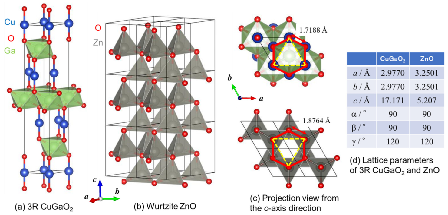
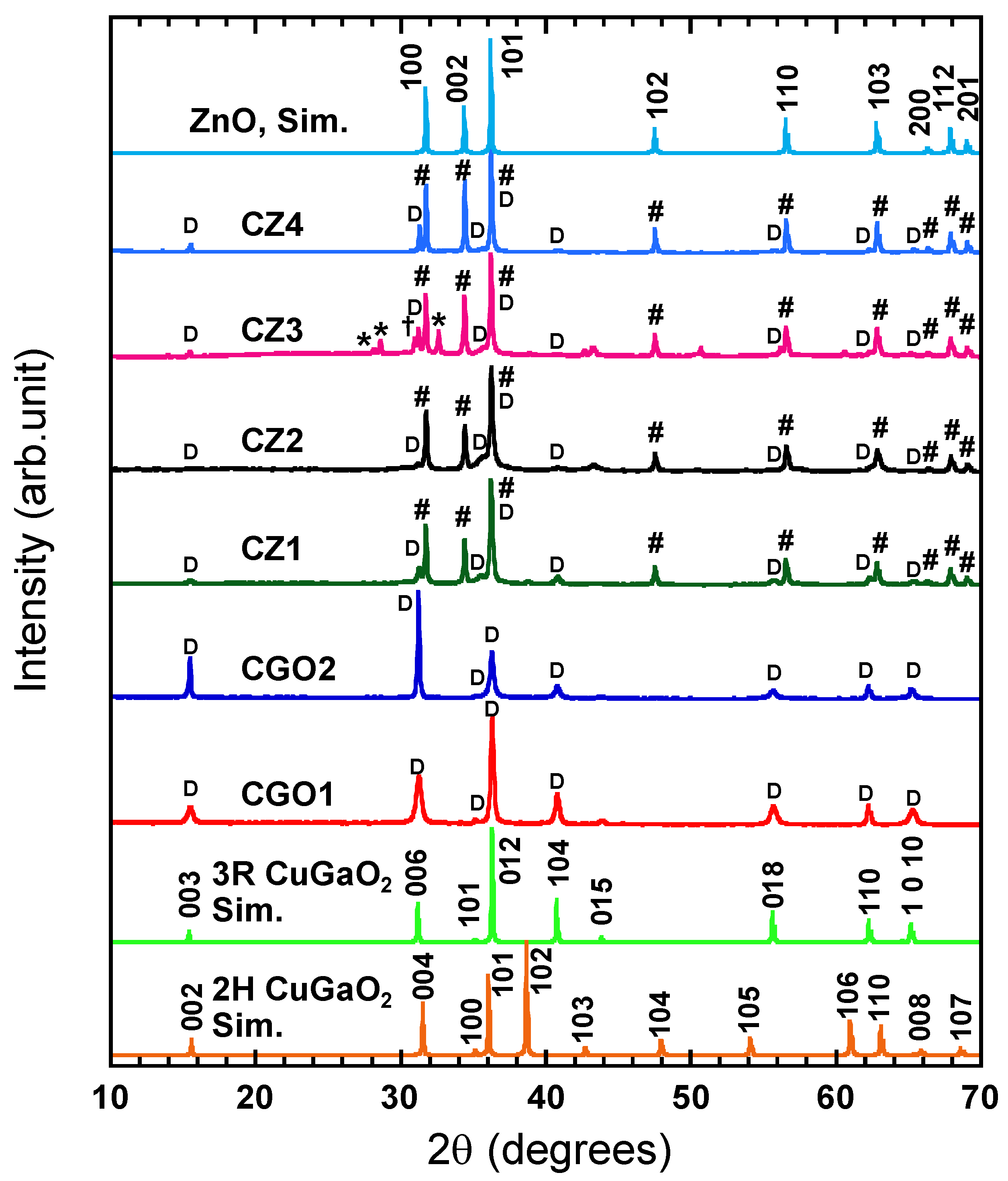
3.1. Structural Analysis of CuGaO2 and CuGaO2/ZnO Hybrids

The structure and morphology of the interfacial CuGaO2/ZnO hybrids were investigated by powder XRD and SEM. The XRD patterns of the hybrids after H2/N2 annealing are shown in Figure 3, together with those of the CGO1 and CGO2 base crystals [9]. The simulated patterns of CuGaO2 (ICDD PDF 01-082-8561 for 3R and ICDD PDF 04-011-1001 for 2H) and ZnO (ICDD PDF 04-003-2106) are also shown for comparison. From the figures of CGO1 and CGO2, it is elucidated that hydrothermal synthesis resulted in the formation of rhombohedral (3R) CuGaO2 as a single phase (signified by “D” in Figure 3). The hydrothermal deposition of ZnO on CuGaO2 generated CuGaO2/ZnO hybrids. As shown in Figure 3, new XRD peaks in CZ1–4 are attributed to wurtzite-type ZnO (indicated by the # symbol). Contrary to the early work [9], a post-reduction process was employed here, i.e., the CZ1-4 samples were heat-treated in a hydrogen atmosphere to induce more carriers in n-type ZnO [37]. For the CZ1–3 samples, where CGO1 was used as a base crystal, the X-ray reflection peaks (#) are superimposed on the peaks (D) corresponding to 3R CuGaO2, and the intensity increases with the amount of Zn(CH3COO)2·2H2O involved in the reaction (see Table 1).
While the XRD peaks of the CZ1 and CZ2 samples are consistent with the results of our previous work [9], the CZ3 sample exceptionally exhibits a small peak at 30.97° (†), which indicates the formation of spinel-type cubic CuGa2O4 (Fd-3m) (ICDD PDF 04-001-9116) [38]. There are also three additional peaks (*) in CZ3, which are not assigned to any single component of copper oxide (Cu2O/CuO) or gallium oxide (Ga2O3) but might be attributed to spinel-type tetragonal ZnCu2O4 (I41/amd) [39,40,41]. (Figure S2 in the ESI.) ZnCu2O4 spinel is not available in nature but has recently been revealed by computational predictions [42,43,44]. This evolution could be specifically promoted during the simultaneous production of CuGa2O4 spinel, as hypothesized by a sequential reaction scheme shown in Figure 4. Before the formation of CuGaO2/ZnO hybrid (CZ3), CuGaO2 partially decomposes in the annealing process in air to CuO and Ga2O3, as seen in Reaction 1 in Figure 4 (confirmed by the Raman and XPS data below). According to Hautier et al. [40], the development of ZnCu2O4 requires a more oxidizing environment. In our case, additional oxygen might be supplied when water molecules were adsorbed on the species during the hydrothermal synthesis of ZnO. If this is the case, partial formation of ZnCu2O4 and CuGa2O4 spinels could occur in the post-reduction process (Reaction 2 in Figure 4), because the XRD patterns of the hybrids before the H2/N2 reduction exhibited only ZnO and CuGaO2 without any additional phases such as ZnCu2O4 and CuGa2O4, as shown in Figure S3 in the ESI.
To look at the CZ4 prepared using CGO2, the sharp (006) peak of CuGaO2 is visible in the XRD pattern, and its relative intensity is high than that of the (104) peak in the same crystal (I006/I104 = 13.1, which is closer to I006/I104 = 7.57 for CGO2 than I006/I104 =1.57 for CGO1), suggesting the effective deposition of ZnO on the c plane (006) of the CuGaO2 platelets in CZ4. (See Figure S4 in the ESI.)
Small peaks at ~43°, ~50°, and ~61° are distinct in the XRD patterns of CZ2 and CZ3 (Figure 3) but are absent in the XRD patterns of the same hybrids before the post-reduction process [9]. From a database survey, they were assignable to Cu2O and metallic Cu with face-centered cubic and hexagonal structures, respectively, as shown in Figure S2, and Table S1 in the ESI.

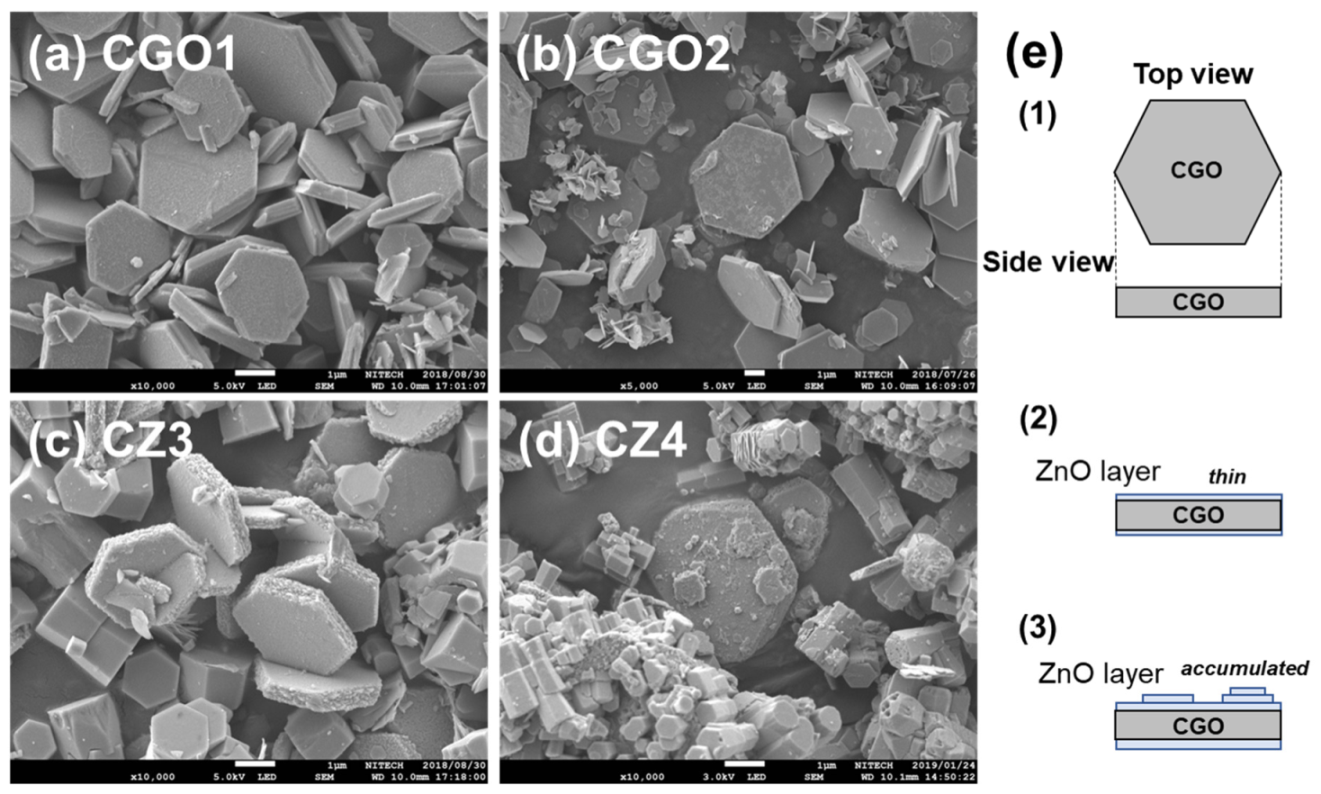
3.2. SEM Observation of CuGaO2 and CuGaO2/ZnO Hybrids

Figure 5 shows the SEM images of CuGaO2 and CuGaO2/ZnO hybrids samples. The CuGaO2 base crystals exhibit well-defined and characteristic morphologies of hexagonal plates with sizes of 1–3 μm [CGO1, Figure 5a] and 5–8 μm [CGO2, Figure 5b]. The variations in size are related to the molecular weight of the PEG used in the synthesis [9]. For CGO2 when PEG 20,000 was used, the XRD peak corresponding to the (006) plane was relatively strong, indicating an enhanced growth of hexagonal plate-like particles. Because more –C–O–C– moieties are available in the PEG with higher molecular weight, more adsorption occurs on the (006) plane, and the growth of the c plane is promoted [9].
SEM investigation of the hybrids synthesized with various amounts of Zn(CH3COO)2·2H2O elucidates that the morphological results of the samples are dependent on the starting base crystals. Here, SEM images of CZ3 ([Zn]/[Cu] = 11) and CZ4 ([Zn]/[Cu] = 16.5) are shown in Figure 5c,d. (SEM images of the CZ1 and CZ2 samples are given in Figure S5 in the ESI.) Unlike CZ1 and CZ2, the surfaces of the plate-like CuGaO2 particles in CZ3 (Figure 5c) are completely covered with a ZnO layer. As for CZ4 (Figure 5d), which was hybridized with the larger CGO2 base crystal, the ZnO well covers the hexagonal CuGaO2 particles to form a thick layer, and individual ZnO hexagonal blocks are also observed. A variety of ZnO layering on the CuGaO2 plate is illustrated in Figure 5e. SEM-EDS results for the hybrids, shown in Figures S6–S9 in the ESI, indeed reveal the presence of ZnO on the CuGaO2 platelets [45].

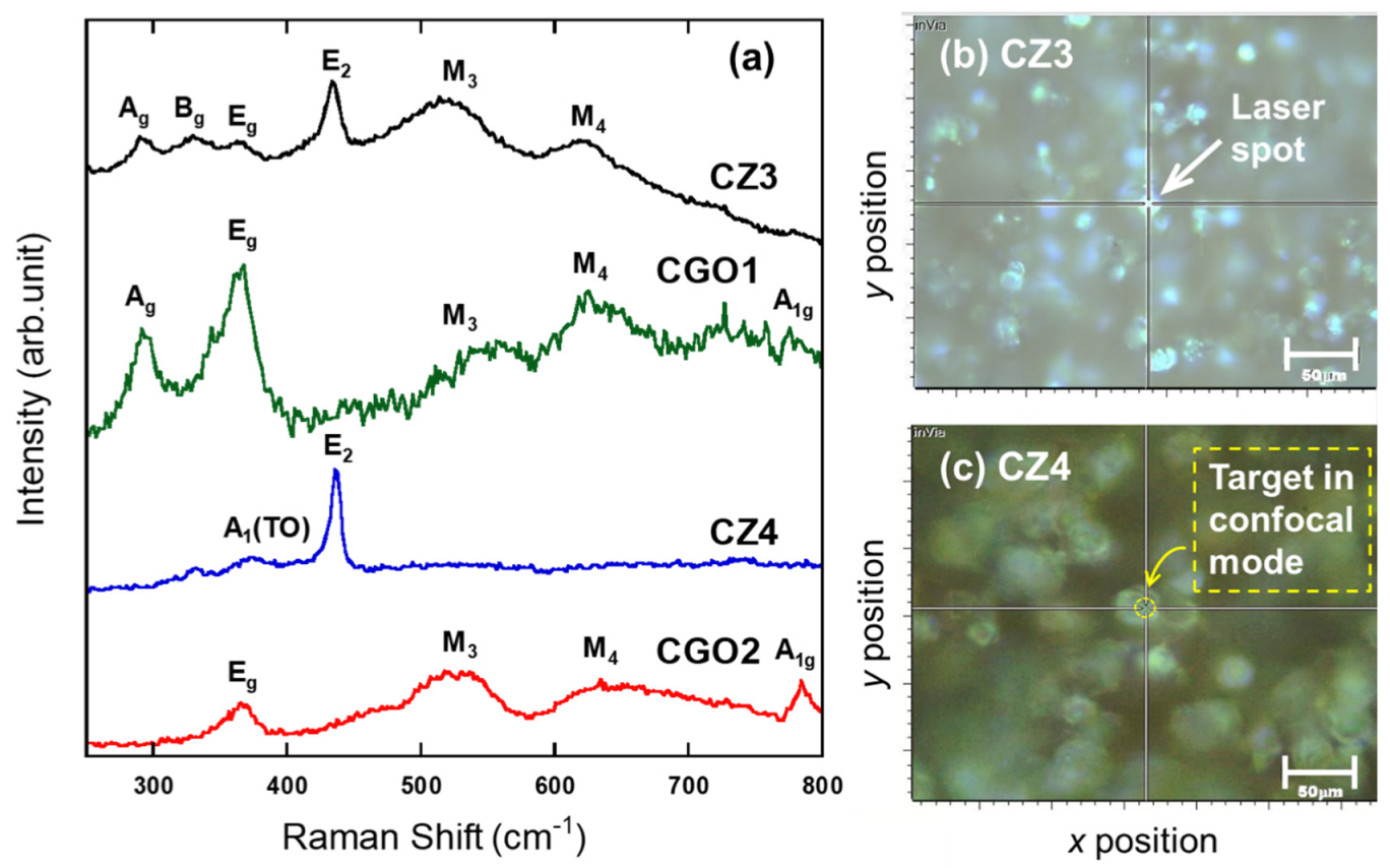
3.3. Micro-Raman Investigation

Micro-Raman spectra of CGO1, CGO2, CZ3, and CZ4 are shown in Figure 6a. A Raman microscope was used for the measurement and a hexagonal platelet was imaged with a 100× objective. The optical pictures recorded during the spectral measurements are shown in Figure 6b,c. The laser wavelength was 532 nm, and the depth of the irradiated spot was approximately 1 μm because the measurement was performed in the confocal mode (See Figure 6d–f) [46]. The beam spot size was estimated to be ~2 μm ϕ , which was small enough to detect the Raman signal of a single CuGaO2 (size 3~8 μm) and CuGaO2/ZnO plates. (Figure 6d) As shown in Figure 6a, Raman signals corresponding to CuGaO2 [28] were obtained in CGO1, CGO2, and CZ3, and a signal attributed to ZnO was confirmed [47] in CZ3 and CZ4.
Looking closer, Raman spectra of CGO1 and CGO2 exhibit peaks corresponding to the Eg, M3, M4, and A1g modes of delafossite CuGaO2 crystals [28], observed at approximately 380, 521, 610, and 780 cm−1, respectively. According to the literature [28], the modes labeled as M3 and M4 are attributed to the stress-induced modes of Ag (and/or Bu) and Bu at the X point, respectively, meaning that our observations may be specific to the hydrothermal synthesis of CuGaO2. For CGO1 and CZ3, Raman peaks with lower wavenumbers are very similar to the vibrational modes of CuO (Ag and Bg) [48], suggesting the partial decomposition of CuGaO2, as discussed with Reaction 1 in Figure 4. Moreover, the observed CuGaO2 peaks in the CZ3 sample shift slightly to lower wavenumbers. This shift is caused by the distortion of the CuGaO2 crystal induced by strains at the hetero-interface between CuGaO2 and ZnO (see the discussion on XPS results shown later). In the Raman spectra of CZ3 and CZ4, a signal at 435 cm−1 is observed that was correlated to the E2 mode of ZnO on the CuGaO2 plate. In CZ4, a small peak at ~380 cm−1 emerged and was assigned to the A1(TO) mode of ZnO [47,49]. These ZnO-related modes confirm that CuGaO2 was successfully hybridized with ZnO. As for the CZ3 sample, Raman signals from the CuGaO2 plate are also detected in addition to the ZnO peaks, because the ZnO layer is less than 1 μm thickness (See Figure 5e(2) and Figure 6e). Contrarily, CZ4 has thicker, accumulated ZnO layers (See Figure 5e(3)), and no vibrational modes of CuGaO2 are visible in the Raman spectrum apart from a strong ZnO peak (See Figure 6f). Many isolated ZnO blocks appear around the hybrid because the highest Zn(CH3COO)2·2H2O content was used ([Zn]/[Cu] = 16.5) in CZ4, which is in agreement with the XRD results. A comparison of the SEM images of CZ3 and CZ4 confirms that small hexagonal blocks of ZnO are formed and accumulate on the surface of the CGO2 plates in CZ4, while CZ3 has a thinner ZnO coating on the CGO1 particles. In our previous study, we found that CZ4 had better photocatalytic properties because the larger CuGaO2 hexagonal plates were well-coated with ZnO [45]. Hence, a sufficient thickness of the ZnO layer would be important to extract electrons from electron-hole pairs generated at the p-n interface between CuGaO2 and ZnO and prevent electrons from returning to the interface with p-type CuGaO2, resulting in the higher photocatalytic performance, as demonstrated in our previous study.

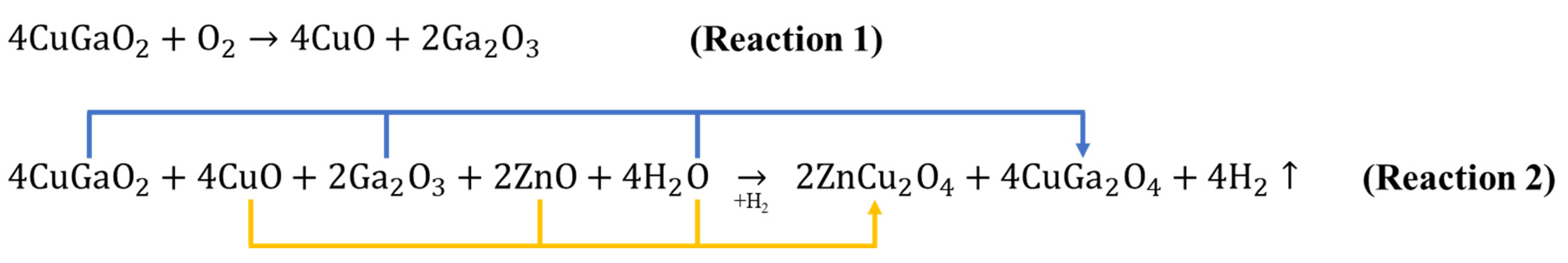
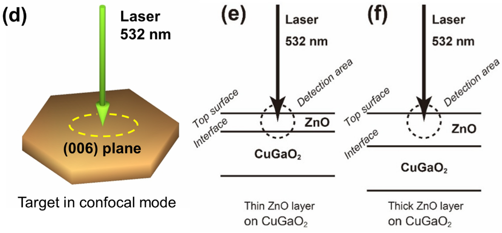
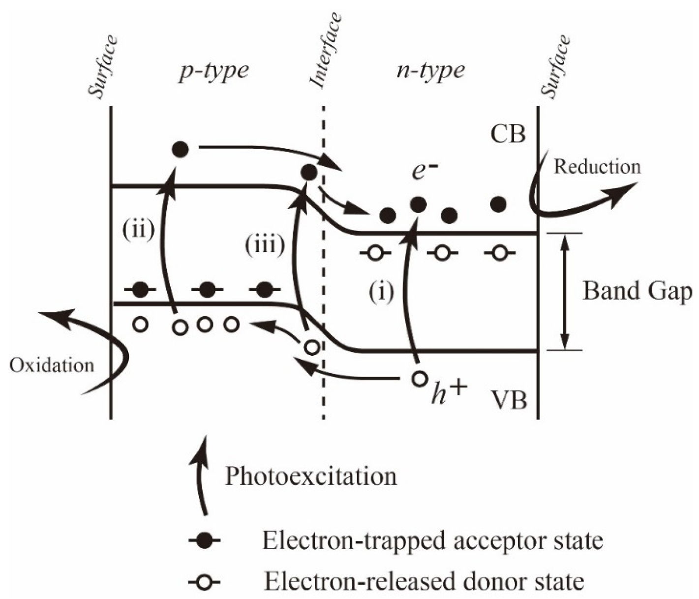
3.4. Unique Reaction in the Boundary between CuGaO2 and ZnO in CZ3

As seen in Section 3.1, the CZ3 samples experienced the crystallization of two spinel phases. Here, the formation mechanism of ZnCu2O4 and CuGa2O4 shall be discussed. Firstly, to be mentioned, the particle size of CGO has a significant impact on the formation of ZnCu2O4 and CuGa2O4; CGO1 and CGO2 were prepared using PEG 6000 and PEG 20,000, respectively. Compared with CGO2, CGO1 has a smaller size, indicating that it has a higher specific surface area [45]. Therefore, more oxygen molecules are likely to be adsorbed on CGO1 and more dominantly trigger the decomposition reaction. For the CZ3 sample synthesized with [Zn]/[Cu] ratio = 11 and CGO1 used, CuO and Ga2O3 produced by the partial decomposition may react with excess ZnO to develop ZnCu2O4 and CuGa2O4 during the post-reduction process according to Reactions 1 and 2, as shown in Figure 4. In comparison, when [Zn]/[Cu] ratio maintains as 11 and CGO2 is used instead of CGO1, the XRD pattern (Figure S10 in the ESI) only shows peaks of ZnO and CuGaO2, while those attributed to ZnCu2O4 and CuGa2O4 are not detected. It indicates that increasing the particle size of CuGaO2 significantly reduces the number of oxygen molecules adsorbed on the hexagonal platelets for partial decomposition, which leads to the production of small amounts of ZnCu2O4 and CuGa2O4 phases in the subsequent reduction process and leads to more efficient hybridization with ZnO.
The spinel synthesis in CuGaO2/ZnO hybrid is itself interesting. However, to take into consideration the results of XRD, SEM, and Raman investigations, a further experiment of XPS is determined to be performed for the CZ4 and pristine CGO2 base crystal because the CZ sample possesses the sufficient ZnO layer without any additional phases like CuO and the spinels suspected to hinder the carrier separation in the boundary between CuGaO2 and ZnO.

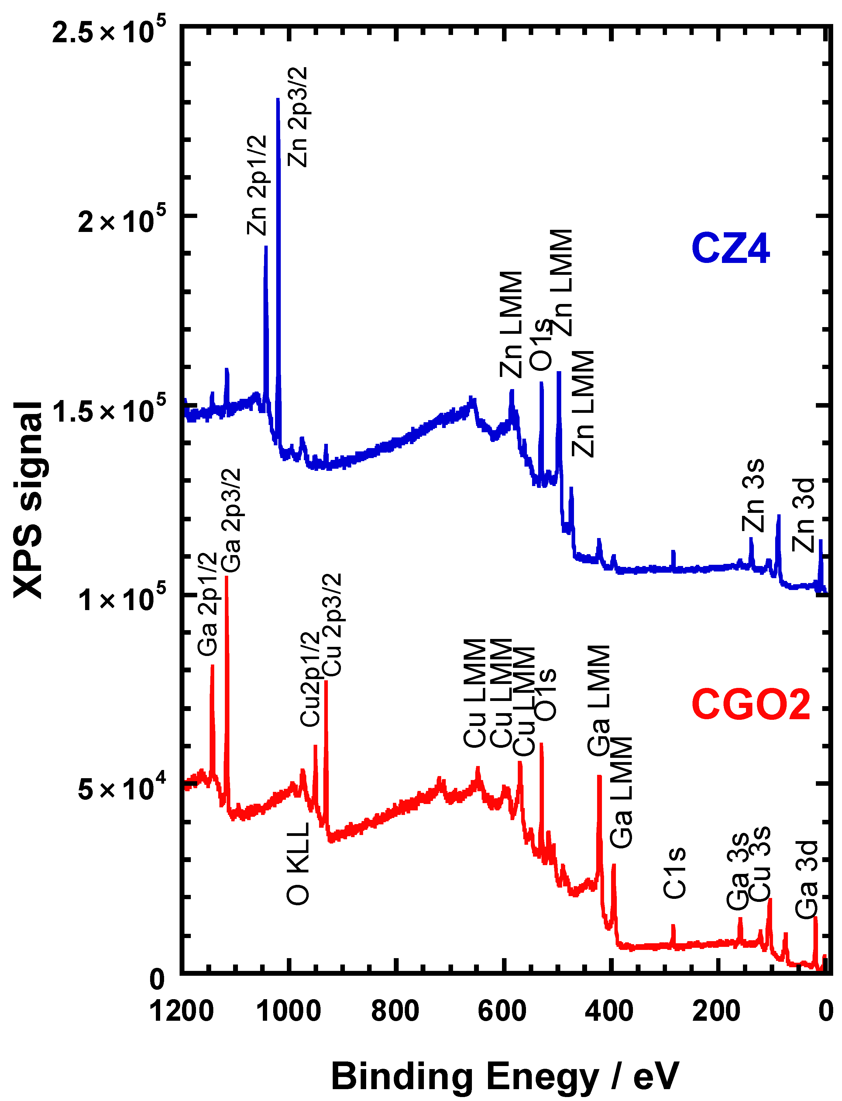
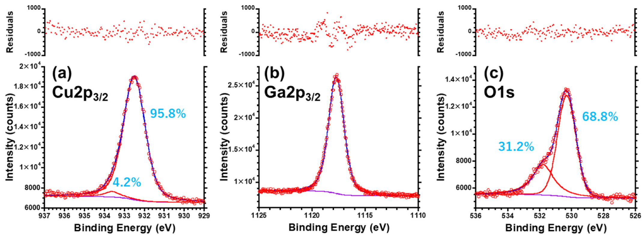
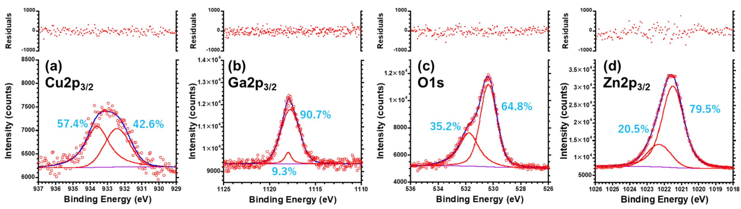
3.5. XPS Analysis for the CuGaO2 Base Crystal and CuGaO2/ZnO Hybrid

A broad scan XPS spectrum is obtained to identify the elements in the respective sample. Figure 7 shows the comparison of the wide-scan spectra of CGO2 and CZ4. The photoelectron peaks of the main constituents, Cu, Ga, Zn, and O and Auger Cu, Ga, Zn LMM, and O KLL peaks are observed, wherein Cu 2 p 3 / 2 and Cu 2 p 1 / 2 were detected at 932 and 952 ev [50], respectively; Ga 2 p 3 / 2 and Ga 2 p 1 / 2 at 1117 and 1144 eV [51], respectively, and O 1 s at approximately 530 eV [52]. The XPS peaks of Zn were detected only for CZ4 and were assigned to Zn 2 p 3 / 2 and Zn 2 p 1 / 2 (1021.5 and 1044.5 eV, respectively) [53,54]. The positions and width of the detected XPS peaks were tabled in Table 2.
Figure 8a and Figure 9a show the Cu 2 p 3 / 2 XPS CL spectra of CGO2 and CZ4, respectively. After subtracting the Shirley background, the experimental peak at 932.5 eV was fitted with Voigt functions using Igor Pro 8.0 software. At first, the chemical state of Cu in CGO2 was analyzed in detail by investigating Cu 2 p 3 / 2 XPS CL signal [55]. Although it seemed possible to be fitted with a single Voigt function peaked at 932.5 eV assignable to Cu+ ions, the addition of the second Voigt function at 933.6 eV for Cu2+ state provided a more reliable fitting result, which can elucidate the influence of Cu2+ ions in this substance. As seen in Figure 8a, the ratio of Cu2+ ions is low enough ~4%. On the other hand, the Cu XPS signal for CZ4 in Figure 9a is found to be very broadened (full width at half maximum (FWHM) ~2.4 eV) in comparison with that of CGO2 (FWHM ~1.2 eV), and well fitted with two Voigt functions peaked at 932.4 eV for Cu+ and 933.6 eV for Cu2+ ions. The analytical data are listed in Table 3. The feature was not varied after surface etching by argon ion beam sputtering. The equivalent amount of Cu2+ to Cu+ ions is detected for the CZ4 sample.
The copper valence state of CuGaO2 base crystal was also estimated by modified Auger parameter α , defined by the following equation [56]:
α = α + h v = ( K E A u g e r   e l e c t r o n K E p h o t o e l e c t r o n ) + h v                                           = K E A u g e r   e l e c t r o n + B E p h o t o e l e c t r o n
where h v is the photon energy of the exciting radiation, KEs are the kinetic energies of Auger electron and photoelectron, and BE is the binding energy of the photoelectron from the CL level of the targeted element. The Cu L3M4,5M4,5 peak is detected at 916.63 eV for CGO2 (the magnified figure is given in Figure S1a in the ESI), and the Auger parameter is estimated to be 1849.14 eV. Table 4 shows the XPS CL peak location and α for CGO2, compared with literature data of various copper compounds. They are found to be well matched to those of Cu2O [55,57,58], resulting in that the CGO2 was composed of well-defined Cu+ monovalent ions. As for CZ4, unfortunately, Auger peak Cu LMM was not available because of its weakness and/or broadening of the corresponding peak. Nevertheless, the binding energy of the XPS CL signal sufficiently suggests the presence of Cu2+ ions in the boundary between CuGaO2 and ZnO, resulting from the annealing in air before the formation of a structural hybrid for CuGaO2 and ZnO or an electronic potential slope in the interface region between CuGaO2 and ZnO, inducing the carrier separation as expected.
Regarding the Ga element of the CGO2 compound (Figure 8b), the Ga 2 p 3 / 2 the peak at 1117 eV is fitted with a single Voigt function with a shape parameter, defined by a ratio of Lorentzian component width to Gaussian component width, of 0.5 (Gaussian:66.3%, Lorentzian:33.7%). (See Table 3) On the other hand, two Voigt functions are used for CZ4 to obtain a good fit (Figure 9b), which is composed of the main peak (90.7%) at 1117.76 eV with a small, relatively sharp peak at 1117.98 eV (9.3%). The small peak was also detected in the measurement of depth profiles of Ga 2 p 3 / 2 XPS CL spectra for the CuGaO2/ZnO hybrid, thus indicative of a specific state of Ga-O bonds in a boundary between CuGaO2 and ZnO. A comparison of the present data with the binding energies of metallic Ga (1116 eV) [59,60] and Ga2O3 (1118 eV) [51,60] reveals that the observed XPS peaks cannot be attributed to the lower valence state of Ga and the Ga elements resultantly have to be in a trivalent state coordinated with oxygens. As shown in Figure 8a,b and Figure 9a,b, the Cu and Ga XPS CL signals of the hybrid samples are quite small because of the formation of the ZnO layer on CuGaO2. However, a meaningful deconvolution analysis can be performed. Interestingly, the analysis of the Ga2p peak of the hybrid shows a larger FWHM (~2.3 eV), significantly broadened in comparison with a sharp peak of ~1.7 eV width for the CGO2 sample (See Table 2), suggesting the formation of the CuGaO2/ZnO hybrid. This means that, while the CGO2 base crystal was composed of distorted but crystallographically-regulated GaO6 octahedra, the CZ4 hybrid possessed GaO6 octahedra with strained chemical bonding states in the boundary region with ZnO. Conclusively, the sufficient ZnO coverage of CuGaO2, as also seen in the SEM image, weakened the XPS signals, but the detected signals are sensitively reflected by chemical states of GaO6 octahedra influenced by the formation of the heterostructure with ZnO.
Ga L3M4,5M4,5 kinetic energies for CGO2 and CZ4 are given in Table 5 and Figure S11b in the ESI. The estimated Auger parameter α values are 2208.7 eV (CGO2) and 2208.2 eV (CZ4), which are not yet reported in the literature so far, and found to be 28 eV higher than that of Ga2O3 (2180.4 eV) [60]. Since “the change in the Auger parameter for a given element is equal to the change in polarization energy of the structure” [56], this will be characteristic of p-type semiconductive CuGaO2 crystal.
Regarding the oxygen, the O1s peak is coherently deconvoluted into two Voigt functions, O#1 (530.3 eV) and O#2 (531.8 eV), and the O1s peak in CuGaO2 [Figure 8c] is composed of 68.8% O#1 and 31.2% O#2. For the CZ4 hybrid [Figure 9c], the O1s is 64.8% O#1 and 35.2% O#2, and has the same trend. According to the literature, adsorbed H2O molecules and OH moieties are related to XPS peaks at 532.8 and 531.7 eV, respectively [52,61]. Thus, the O#2 signals for CGO2 and CZ4 are attributed to OH moieties owing to the hydrothermal synthesis. On the other hand, the observed binding energy for O#1 in these samples should originate from O as the main framework in the CuGaO2 and ZnO structures. However, the chemical states are different between CuGaO2 and ZnO because ZnO layer has four-fold coordinated oxygen with Zn (OZn4), whereas in CuGaO2, oxygen has four-fold-coordination with Cu and three Ga atoms combined with the GaO6 octahedron, that is, an OCuGa3 tetrahedron is present [Figures S1a and S12 in the ESI]. The broad feature of the O1s peak did not enable the different environments to distinguish.
Zn XPS signals were observed only for CZ4. As shown in Figure 9d, the Zn 2 p 3 / 2 peak at 1021.7 eV is deconvoluted into two Voigt functions of Zn#1 at 1021.5 eV by 79.5% and Zn#2 at 1022.3 eV by 20.5%. In comparison with literature data including Zn (1021.8 eV) [56,57], ZnO (1022.1 eV) [57,62], and CuZn (1021.5 eV) [57], the obtained binding energy of Zn#1 appears to show rather lower valence state for the Zn element of the CZ4 sample, except for Zn#2 corresponding to a divalent state (Zn2+) of the individual ZnO bulky blocks seen in the SEM image (Figure 5d). However, this discrepancy can be elucidated by the analysis of the modified Auger parameter α . The Auger parameters for Zn element of various materials (Zn, ZnO, CuZn, and Al-doped ZnO(AZO)) are compared in Table 6 with the present data for CZ4 given from the data of Auger peak Zn L3M45M45 (See Figure S11c). It is seen that the value of the CZ4 hybrid ( α = 2010.1 eV) is equivalent to ZnO ( α = 2010.3 eV) [57,62] and Al-doped ZnO ( α = 2009.4 eV) [63] and rather distinguishable from those of metallic Zn and alloy CuZn ( α = 2013.9 eV) [57,62]. The results will be explained by the formation of a structural hybrid of CuGaO2 and ZnO, which would induce effective transport of electron carriers to the ZnO region from the hetero-interface between the ZnO layer and CuGaO2 crystal, like Cu2O/ZnO and CuO/ZnO hetero-interfaces (See Table 6) [64].
In summary, the CuGaO2/ZnO hybrid was formed with a ZnO layer on the CuGaO2 hexagonal platelet particles. The analysis of Cu and Ga 2p3/2 XPS CL signals suggested the presence of Cu2+ ions and strained GaO6 octahedra in the boundary between CuGaO2 and ZnO. The Zn 2p3/2 binding energy and modified Auger parameter unveiled a unique specification of the hybrid sample, indicating the possibility of CuGaO2/ZnO hetero-interface as a p-n type catalyst.

4. Conclusions

Hydrothermally synthesized CuGaO2/ZnO hybrids, which were formed with CuGaO2 hexagonal-plate base crystal and ZnO layer, were investigated. XRD and SEM investigations confirmed the successful deposition of ZnO on the CuGaO2 plate, and the subsequent reduction process induced an extraordinary reaction in the interface between CuGaO2 and ZnO, which could be tuned out by varying the particle size of CuGaO2 and [Zn]/[Cu] ratio. Micro-Raman observations confirmed the vibrational modes of ZnO in the CuGaO2/ZnO hybrids. XPS profiles showed the presence of Cu, Ga, and O in the CuGaO2 and of Zn in the CuGaO2/ZnO hybrids in addition to the elements from the base crystal, and the quantitative analysis of valence states of Cu ions (Cu+ and Cu2+) was performed. The Cu2+ ratio was characteristically higher in the hybrids than in the CuGaO2 crystal. The Ga XP spectra indicated that the GaO6 octahedra in the inner structure of the CuGaO2 base crystal were crystallographically well-constructed, while more strains were involved in the hetero-interface between CuGaO2 and ZnO. The electronic state of the CuGaO2/ZnO hybrid was found to be significantly influenced by the formation of the hetero-interface between CuGaO2 and ZnO in the analysis of the Zn XPS CL binding energies and modified Auger parameters, indicating effective transport of electron carriers to the ZnO region from the hetero-interface. It was concluded that the hydrothermal approach for the hybrid compound synthesis was promising and could cut out a new path for the development of optoelectronic devices.

Supplementary Materials

The following supporting information can be downloaded at: https://www.mdpi.com/article/10.3390/ceramics5040048/s1. Figure S1 (a): Extracted crystal structure of rhombohedral CuGaO2 (R-3m). Blue, red, and green balls show Cu, O, Ga elements, respectively. The lattice parameters are taken from ICDD PDF 01-082-8561; Figure S1 (b): Extracted crystal structure of wurtzite(hexagonal) ZnO (P63mc). Grey and red balls show Zn and O elements, respectively. The lattice parameters are taken from ICDD PDF 04-003-2106; Figure S2: XRD pattern of CZ3 sample (after the H2 annealing process) and assignment of the corresponding crystals; Table S1: XRD peak assignment for the CZ3 sample; Figure S3: XRD patterns of CuGaO2/ZnO hybrids of CZ1-4 before the H2 annealing process. (#:wurtzite ZnO, D:rhombohedral(3R) CuGaO2); Figure S4: XRD pattern (magnified) of CZ4 sample after the H2 annealing process; Figure S5: SEM images of the CZ1 (a) and CZ2 (b) samples; Figure S6: SEM-EDS results of the CZ1 sample; Figure S7: SEM-EDS results of the CZ2 sample; Figure S8: SEM-EDS results of the CZ3 sample; Figure S9: SEM-EDS results of the CZ4 sample, which are taken, for comparison with Figures S5–S7, from the literature, Ref. [45] (M. Choi, S. Yagi, Y. Ohta, K. Kido and T. Hayakawa, J. Phys. Chem. Solids, 150 (2021) 109845); Figure S10: Comparison of XRD patterns for two CuGaO2/ZnO hybris synthesized with the same [Zn]/[Cu] ratio (=11) but by use of the different base crystals, CGO1 and CGO2 (#:wurtzite ZnO, D:rhombohedral(3R) CuGaO2); Figure S11: Auger L3M4,5M4,5 spectra for CGO2 ((a) Cu LMM and (b) Ga LMM) and CZ4 ((b) Ga LMM and (c) Zn LMM); Figure S12: Overview of OCuGa3 polyhedra in 3R CuGaO2 structure.

Author Contributions

M.C.: investigation, writing the original draft, data curation, and visualization. C.B.: supervision, project administration. T.H.: conceptualization, methodology, resources, data curation, formal analysis, visualization, supervision, validation, writing—review and editing, and project administration. All authors have read and agreed to the published version of the manuscript.

Funding

This work was supported by grants from the Frontier Research Institute of Materials Science (FRIMS) of the Nagoya Institute of Technology and the Deutsche Forschungsgemeinschaft under GRK2495/E.

Institutional Review Board Statement

Not applicable.

Informed Consent Statement

Not applicable.

Data Availability Statement

The datasets used and/or analysed during the current study are available from the corresponding author upon reasonable request.

Conflicts of Interest

There are no conflict to declare.

References

  1. Chen, X.; Shen, S.; Guo, L.; Mao, S.S. Semiconductor-based photocatalytic hydrogen generation. Chem. Rev. 2010, 110, 6503–6570. [Google Scholar] [CrossRef] [PubMed]
  2. Mills, A.; Davies, R.H.; Worsley, D. Water purification by semiconductor photocatalysis. Chem. Soc. Rev. 1993, 22, 417–425. [Google Scholar] [CrossRef]
  3. Yu, M.; Natu, G.; Ji, Z.; Wu, Y. p-Type dye-sensitized solar cells based on delafossite CuGaO2 nanoplates with saturation photovoltages exceeding 460 mV. J. Phys. Chem. Lett. 2012, 3, 1074–1078. [Google Scholar] [CrossRef] [PubMed]
  4. Li, J.; Fang, W.; Yu, C.; Zhou, W.; Zhu, L.; Xie, Y. Ag-based semiconductor photocatalysts in environmental purification. Appl. Surf. Sci. 2015, 358, 46–56. [Google Scholar] [CrossRef]
  5. Ke, J.; Younis, M.A.; Kong, Y.; Zhou, H.; Liu, J.; Lei, L.; Hou, Y. Nanostructured ternary metal tungstate-based photocatalysts for environmental purification and solar water splitting: A review. Nano-Micro Lett. 2018, 10, 69. [Google Scholar] [CrossRef]
  6. Zhao, R.D.; Zhang, Y.M.; Liu, Q.L.; Zhao, Z.Y. Effects of the preparation process on the photocatalytic performance of delafossite CuCrO2. Inorg. Chem. 2020, 59, 16679–16689. [Google Scholar] [CrossRef]
  7. Kumar, M.; Zhao, H.; Persson, C. Study of band-structure, optical properties and native defects in AIBIIIO2 (AI=Cu or Ag, BIII=Al, Ga or In) delafossite. Semicond. Sci. Technol. 2013, 28, 065003. [Google Scholar] [CrossRef]
  8. Bredar, A.R.C.; Blanchet, M.D.; Comes, R.B.; Farnum, B.H. Evidence and influence of copper vacancies in p-type CuGaO2 mesoporous films. ACS Appl. Energy Mater. 2019, 2, 19–28. [Google Scholar] [CrossRef]
  9. Choi, M.U.; Hayakawa, T. Hydrothermal synthesis and photocatalytic properties of CuGaO2/ZnO hexagonal platelet hybrids. Mater. Res. Bull. 2019, 113, 84–89. [Google Scholar] [CrossRef]
  10. Wang, J.; Ibarra, V.; Barrera, D.; Xu, L.; Lee, Y.J.; Hsu, J.W.P. Solution synthesized p-type copper gallium oxide nanoplates as hole transport layer for organic photovoltaic devices. J. Phys. Chem. Lett. 2015, 6, 1071–1075. [Google Scholar] [CrossRef]
  11. Suzuki, I.; Nagatani, H.; Kita, M.; Iguchi, Y.; Sato, C.; Yanagi, H.; Ohashi, N.; Omata, T. First-principles study of CuGaO2 polymorphs: Delafossite α-CuGaO2 and wurtzite β-CuGaO2. Inorg. Chem. 2016, 55, 7610–7616. [Google Scholar] [CrossRef] [PubMed]
  12. Xu, Z.; Xiong, D.; Wang, H.; Zhang, W.; Zeng, X.; Ming, L.; Chen, W.; Xu, X.; Cui, J.; Wang, M.; et al. Remarkable photocurrent of p-type dye-sensitized solar cell achieved by size controlled CuGaO2 nanoplates. J. Mater. Chem. A 2014, 2, 2968–2976. [Google Scholar] [CrossRef]
  13. Ehara, T. Preparation of CuGaO2 thin film by a sol-gel method using two kinds of metal source combination. J. Mater. Sci. Chem. Eng. 2018, 6, 68–78. [Google Scholar]
  14. Xu, Y.; Ma, G.; Wang, G.; Shi, L.; Zhang, H.; Jin, L.; Ma, X.; Zou, Y.; Yin, J.; Li, Y. Interface state luminescence and sub-bandgap absorption based on CuGaO2 nanoplates/ZnO nanowires heterostructure arrays. Phys. Status Solidi B 2018, 255, 1800391. [Google Scholar] [CrossRef]
  15. Abrahams, S.C.; Bernstein, J.L. Remeasurement of the structure of hexagonal ZnO. Acta Cryst. B 1969, 25, 1233–1236. [Google Scholar] [CrossRef]
  16. Zhang, Z.; Yates, J.T., Jr. Band bending in semiconductors: Chemical and physical consequences at surfaces and interfaces. Chem. Rev. 2012, 112, 5520–5551. [Google Scholar] [CrossRef]
  17. Pirhashemi, M.; Habibi-Yangjeh, A.; Pouran, S.R. Review on the criteria anticipated for the fabrication of highly efficient ZnO-based visible-light-driven photocatalysts. J. Ind. Eng. Chem. 2018, 62, 1–25. [Google Scholar] [CrossRef]
  18. Dong, S.; Feng, J.; Fan, M.; Pi, Y.; Hu, L.; Han, X.; Liu, M.; Sun, J.; Sun, J. Recent developments in heterogeneous photocatalytic water treatment using visible light responsive photocatalysts: A review. RSC Adv. 2015, 5, 14610. [Google Scholar] [CrossRef]
  19. Han, M.; Lu, Y.; Liu, Y.; Hu, Z.; Chen, G.; Jiang, K.; Zhang, J.; Li, W. Raman scattering measurements of phonon anharmonicity in the delafossite CuGa1−xCrxO2 (0 ≤ x ≤ 1) films. J. Raman Spectrosc. 2020, 51, 851–859. [Google Scholar] [CrossRef]
  20. Wang, H.; Mann, C.K.; Vickers, T.J. Effect of powder properties on the intensity of Raman scattering by crystalline solids. Appl. Spectrosc. 2002, 56, 1538–1544. [Google Scholar] [CrossRef]
  21. Wirths, S.; Tiedemann, A.T.; Ikonic, Z.; Harrison, P.; Holländer, B.; Stoica, T.; Mussler, G.; Myronov, M.; Hartmann, J.M.; Grützmacher, D.; et al. Band engineering and growth of tensile strained Ge/(Si) GeSn heterostructures for tunnel field effect transistors. Appl. Phys. Lett. 2013, 102, 192103. [Google Scholar] [CrossRef] [Green Version]
  22. Laurentius, L.; Stoyanov, S.R.; Gusarov, S.; Kovalenko, A.; Du, R.; Lopinski, G.P.; McDermott, M.T. Diazonium-derived aryl films on gold nanoparticles: Evidence for a carbon-gold covalent bond. ACS Nano 2011, 5, 4219–4227. [Google Scholar] [CrossRef] [PubMed]
  23. Bood, J.; Brackmann, C.; Bengtsson, P.-E.; Aldén, M. Multipoint temperature and oxygen-concentration measurements using rotational coherent anti-Stokes Raman spectroscopy. Opt. Lett. 2000, 25, 1535–1537. [Google Scholar] [CrossRef]
  24. Han, M.J.; Jiang, K.; Zhang, J.Z.; Li, Y.W.; Hu, Z.G.; Chu, J.H. Temperature dependent phonon evolutions and optical properties of highly c-axis oriented CuGaO2 semiconductor films grown by the sol-gel method. Appl. Phys. Lett. 2011, 99, 131104. [Google Scholar]
  25. Ahmed, J.; Mao, Y. Synthesis, characterization and electrocatalytic properties of Delafossite CuGaO2. J. Solid State Chem. 2016, 242, 77–85. [Google Scholar] [CrossRef]
  26. Debbichi, L.; de Lucas, M.C.M.; Pierson, J.F.; Krüger, P. Vibrational properties of CuO and Cu4O3 from first-principles calculations, and Raman and infrared spectroscopy. J. Phys. Chem. C 2012, 116, 10232–10237. [Google Scholar] [CrossRef]
  27. Prabhakaran, G.; Murugan, R. Room temperature ferromagnetic properties of Cu2O microcrystals. J. Alloys Compd. 2013, 579, 572–575. [Google Scholar] [CrossRef]
  28. Pellicer-Porres, J.; Segura, A.; Martínez, E.; Saitta, A.M.; Polian, A.; Chervin, J.C.; Canny, B. Vibrational properties of delafossite CuGaO2 at ambient and high pressures. Phys. Rev. B 2005, 72, 064301. [Google Scholar] [CrossRef]
  29. Gao, H.; Zeng, X.; Guo, Q.; Yang, Z.; Deng, Y.; Li, H.; Xiong, D. P-type transparent conducting characteristics of delafossite Ca doped CuScO2 prepared by hydrothermal synthesis. Dalton Trans. 2021, 50, 5262–5268. [Google Scholar] [CrossRef]
  30. Chen, C.-Y.; Sakthinathan, S.; Yu, C.-L.; Wang, C.-C.; Chiu, T.-W.; Han, Q. Preparation and characterization of delafossite CuCrO2 film on flexible substrate. Ceram. Int. 2021, 47, 23234–23239. [Google Scholar] [CrossRef]
  31. Li, S.; Zhang, X.; Zhang, P.; Sun, X.; Zheng, H.; Zhang, W. Preparation and characterization of solution-processed nanocrystalline p-Type CuAlO2 thin-film transistors. Nanoscale Res. Lett. 2018, 13, 259. [Google Scholar] [CrossRef]
  32. Wu, C.; Qiu, L.; Li, S.; Guo, D.; Li, P.; Wang, S.; Du, P.; Chen, Z.; Liu, A.; Wang, X.; et al. High Sensitive and Stable Solution-Processed All Inorganic Self-powered Solar-blind Photodetector based on CuMO2/Ga2O3 p-n heterojunction. Mater. Today Phys. 2021, 17, 100335. [Google Scholar] [CrossRef]
  33. He, C.; Guo, D.; Chen, K.; Wang, S.; Shen, J.; Zhao, N.; Liu, A.; Zheng, Y.; Li, P.; Wu, Z.; et al. α-Ga2O3 Nanorod Array–Cu2O Microsphere p–n Junctions for Self-Powered Spectrum-Distinguishable Photodetectors. ACS Appl. Nano Mater. 2019, 2, 4095–4103. [Google Scholar] [CrossRef]
  34. Guo, D.; Chen, K.; Wang, S.; Wu, F.; Liu, A.; Li, C.; Li, P.; Tan, C.; Tang, W. Self-Powered Solar-Blind Photodetectors Based on α/β Phase Junction of Ga2O3. Phys. Rev. Applied. 2020, 13, 024051. [Google Scholar] [CrossRef]
  35. Srinivasan, R.; Chavillon, B.; Doussier-Brochard, C.; Cario, L.; Paris, M.; Gautron, E.; Deniard, P.; Odobel, F.; Jobic, S. Tuning the size and color of the p-type wide band gap delafossite semiconductor CuGaO2 with ethylene glycol assisted hydrothermal synthesis. J. Mater. Chem. 2008, 18, 5647–5653. [Google Scholar] [CrossRef]
  36. Izumi, F.; Momma, K. Three-dimensional visualization in powder diffraction. Solid State Phenom. 2007, 130, 15–20. [Google Scholar] [CrossRef]
  37. Huang, J.; Krishna, U.R.; Lemberger, M.; Jank, M.P.M.; Ryssel, H.; Frey, L. Impact of forming gas annealing on ZnO-TFTs. In Proceedings of the 2010 10th IEEE International Conference on Solid-State and Integrated Circuit Technology, Shanghai, China, 1–4 November 2010; pp. 1548–1550. [Google Scholar]
  38. Gingasu, D.; Mindru, I.; Patron, L.; Marinescu, G.; Tuna, F.; Preda, S.; Calderon-Moreno, J.M.; Andronescu, C. Synthesis of CuGa2O4 nanoparticles by precursor and self-propagating combustion method. Ceram. Int. 2012, 38, 6739–6751. [Google Scholar] [CrossRef]
  39. Materials Project: Mp-1541943. Available online: https://materialsproject.org/materials/mp-1541943/ (accessed on 22 September 2021).
  40. Hautier, G.; Fischer, C.C.; Jain, A.; Mueller, T.; Ceder, G. Finding nature’s missing ternary oxide compounds using machine learning and density functional theory. Chem. Mater. 2010, 22, 3762–3767. [Google Scholar] [CrossRef]
  41. Samson, D.O.; Makama, E.K. Effect of Concentration on Morphological, Optical and Electrical Properties of Copper Doped Zinc Oxide Thin Films Deposited by Electrostatic Spray Pyrolysis (ESP) Technique. J. Mater. Sci. Res. Rev. 2018, 1, 24–39. [Google Scholar]
  42. Stoica, M.; Faghaninia, A.; Sun, X.; Lo, C.S. Computational design of p-type transparent conductors for photovoltaic applications. In Proceedings of the IEEE 40th Conference on Photovoltaic Specialists (PVSC), Denver, CO, USA, 8–13 June 2014; pp. 260–265. [Google Scholar] [CrossRef]
  43. Stoica, M.; Lo, C.S. P-type Zinc Oxide Spinels: Application to Transparent Conductors and Spintronics. New J. Phys. 2014, 16, 055011. [Google Scholar] [CrossRef]
  44. Singstock, N.R.; Bartel, C.J.; Holder, A.M.; Musgrave, C.B. High-Throughput Analysis of Materials for Chemical Looping Processes. Adv. Energy Mater. 2020, 10, 2000685. [Google Scholar] [CrossRef]
  45. Choi, M.; Yagi, S.; Ohta, Y.; Kido, K.; Hayakawa, T. Estimation of delafossite p-type CuGaO2/ZnO hybrids as semiconductor photocatalyst by controlling particle size. J. Phys. Chem. Solids 2021, 150, 109845. [Google Scholar] [CrossRef]
  46. Shu, G.; Dai, B.; Ralchenko, V.G.; Khomich, A.A.; Ashkinazi, E.E.; Bolshakov, A.P.; Bokova-Sirosh, S.N.; Liu, K.; Zhao, J.; Han, J.; et al. Epitaxial growth of mosaic diamond: Mapping of stress and defects in crystal junction with a confocal Raman spectroscopy. J. Cryst. Growth 2017, 463, 19–26. [Google Scholar] [CrossRef]
  47. Decremps, F.; Pellicer-Porres, J.; Saitta, A.M.; Chervin, J.C.; Polian, A. High-pressure Raman spectroscopy study of wurtzite ZnO. Phys. Rev. B 2002, 65, 092101. [Google Scholar] [CrossRef]
  48. Litvinchuk, A.P.; Möller, A.; Debbichi, L.; Krüger, P.; Lliev, M.N.; Gospodinov, M.M. Second-ordeRaman scattering in CuO. J. Phys. Condens. Matter 2013, 25, 105402. [Google Scholar] [CrossRef]
  49. Cuscó, R.; Alarcón-Lladó, E.; Ibáñez, J.; Artús, L.; Jiménez, J.; Wang, B.; Callahan, M.J. Temperature dependence of Raman scattering in ZnO. Phys. Rev. B 2007, 75, 165202. [Google Scholar] [CrossRef]
  50. Makhova, L.; Wett, D.; Lorenz, M.; Konovalov, I. X-ray spectroscopic investigation of forbidden direct transitions in CuGaO2 and CuInO2. Phys. Status Solidi 2006, 11, 2861–2866. [Google Scholar] [CrossRef]
  51. Ramana, C.V.; Rubio, E.J.; Barraza, C.D.; Gallardo, A.M.; McPeak, S.; Kotru, S.; Grant, J.T. Chemical bonding, optical constants, and electrical resistivity of sputter-deposited gallium oxide thin films. J. Appl. Phys. 2014, 115, 043508. [Google Scholar] [CrossRef]
  52. Kloprogge, J.T.; Wood, B.J. Systematic XPS study of gallium-substituted boehmite. J. Mater. Sci. 2016, 51, 5436–5444. [Google Scholar] [CrossRef]
  53. Salavati-Niasari, M.; Davar, F.; Khansari, A. Nanosphericals and nanobundles of ZnO: Synthesis and characterization. J. Alloys Compds. 2011, 509, 61–65. [Google Scholar] [CrossRef]
  54. Al-Gaashani, R.; Radiman, S.; Daud, A.R.; Tabet, N.; Al-Douri, Y. XPS and optical studies of different morphologies of ZnO nanostructures prepared by microwave methods. Ceram. Int. 2013, 39, 2283–2292. [Google Scholar] [CrossRef]
  55. Poulston, S.; Parlett, P.M.; Stone, P.; Bowker, M. Surface oxidation and reduction of CuO and Cu2O studied using XPS and XAES. Surf. Interface Anal. 1996, 24, 811–820. [Google Scholar] [CrossRef]
  56. Castle, J.E. A unified scale for the Auger parameter: Methodology and benefits. Suf. Interface Anal. 2022, 54, 455–464. [Google Scholar] [CrossRef]
  57. Deroubaix, G.; Marcus, P. X-ray photoelectron spectroscopy analysis of copper and zinc oxides and sulphides. Surf. Interface Anal. 1992, 18, 39–46. [Google Scholar] [CrossRef]
  58. Biesinger, M.C.; Lau, L.W.M.; Gerson, A.R.; Smart, R.S.C. Resolving surface chemical states in XPS analysis of first row transition metals, oxides, and hydroxides: Sc, Ti, V., Cu and Zn. Appl. Surf. Sci. 2010, 257, 887–898. [Google Scholar] [CrossRef]
  59. Schön, G. Auger and direct electron spectra in X-ray photoelectron studies of zinc, zinc oxide, gallium and gallium oxide. J. Electron Spectrosc. Relat. Phenom. 1973, 2, 75–86. [Google Scholar] [CrossRef]
  60. Borque, J.L.; Biesinger, M.C.; Baines, K.M. Chemical state determination of molecular gallium compounds using XPS. Dalton Trans. 2016, 45, 7678–7696. [Google Scholar] [CrossRef]
  61. Bera, S.; Dhara, S.; Velmurugan, S.; Tyagi, A.K. Analysis on binding energy and Auger parameter for estimating size and stoichiometry of ZnO nanorods. Int. J. Spect. 2012, 2012, 371092. [Google Scholar] [CrossRef]
  62. Dake, L.S.; Baer, D.R.; Zachra, J.M. Auger parameter measurements of zinc compounds relevant to zinc transport in the environment. Surf. Interface Anal. 1989, 14, 14–71. [Google Scholar] [CrossRef]
  63. Islam, M.N.; Ghosh, T.B.; Chopra, K.L.; Acharya, H.N. XPS and X-ray diffraction studies of aluminum-doped zinc oxide transparent conducting films. Thin Solid Films 1996, 280, 20–25. [Google Scholar] [CrossRef]
  64. Jesen, I.J.T.; Gorantla, S.; Løvvik, O.M.; Gan, J.; Nguyen, P.D.; Monakhov, E.; Svensson, B.G.; Gunnæs, A.E.; Diplas, S. Interface phenomena in magnetron sputtered Cu2O/ZnO heterostructures. J. Phys. Condens. Matter. 2017, 29, 435002. [Google Scholar] [CrossRef] [PubMed]
Figure 1. Crystal structures of (a) rhombohedral (3R) CuGaO2 and (b) wurtzite ZnO. (c) Projection views of 3R CuGaO2 (top) and wurtzite ZnO (bottom). (d) Comparison of lattice parameters (a, b, c, α, β, and γ) between 3R CuGaO2 (PDF 01-082-8561) and ZnO (PDF 04-003-2106). Cu and Zn exhibit similar stacking in the c plane, indicating the possibility to form a heterostructure between them via Cu–O–Zn bonding in the c-axis direction.
Ceramics 05 00048 g001
Figure 2. Schematic illustration of photocatalysis mechanism of a heterostructure using p- and n-type semiconductors under light illumination above band-gap energy. The potential slope at the interface between p- and n-type semiconductors can effectively separate generated electron-hole (eh+) pairs. VB: valence band, CB, conduction band. (See the main text about (i)–(iii)).
Ceramics 05 00048 g002
Figure 3. XRD patterns of the CuGaO2/ZnO hybrid samples post-annealed in H2/N2, together with those of the CuGaO2 base crystals (CGO1 and CGO2) for comparison [9]. The simulated patterns of 3R and 2H CuGaO2 and ZnO are also shown. The symbols D, #, †, and * indicate 3R CuGaO2, ZnO, CuGa2O4, and ZnCu2O4, respectively. (See the main text for details.).
Ceramics 05 00048 g003
Figure 4. Reactions for possible formations of ZnCu2O4 and CuGa2O4.
Ceramics 05 00048 g004
Figure 5. SEM images of the CuGaO2 base crystals (a,b) and CuGaO2/ZnO hybrids (c,d). CGO1 (a) was synthesized with PEG 6000 while CGO2 (b) with PEG 20,000. CZ3 (c) and CZ4 (d) were hybridized with CGO1 and COG2, respectively. The scale bar shows 1 μm. [Zn]/[Cu] ratio was adjusted for CZ3 and CZ4, as given in Table 1. (See the details in the Section 2). SEM images of the CZ1 and CZ2 samples can be found in Figure S5 in the ESI. (e) Schematical illustration of ZnO layer on CuGaO2(CGO). (1) bare CGO in top and side views, (2) CGO with thin ZnO layers, and (3) CGO with thicker, rather accumulated ZnO layers in side view.
Ceramics 05 00048 g005
Figure 6. (a) Raman spectra of CuGaO2 and CuGaO2/ZnO, and optical microscopy images of (b) CZ3 and (c) CZ4. The scale bar is 50 μm. (d) Illustration of micro-Raman experiment and (e,f) schematic drawings of depth region for the confocal Raman detection.
Ceramics 05 00048 g006aCeramics 05 00048 g006b
Figure 7. The survey scan spectra of the CGO2 base crystal and CZ4 hybrid.
Ceramics 05 00048 g007
Figure 8. XPS spectra of (a) Cu 2 p 3 / 2 , (b) Ga 2 p 3 / 2 , and (c) O 1 s CLs for the CGO2 base crystal and fitting results using Voigt functions. The fitting results are summarized in Table 3.
Ceramics 05 00048 g008
Figure 9. XPS spectra of (a) Cu 2 p 3 / 2 , (b) Ga 2 p 3 / 2 , (c) O 1 s , and (d) Zn 2 p 3 / 2 CLs for the CZ hybrid sample and fitting results using Voigt functions. The fitting results are summarized in Table 3.
Ceramics 05 00048 g009
Table 1. Sample names and synthesis conditions for CuGaO2/ZnO hybrids. (ac = CH3COO).
Sample NameCuGaO2 UsedMass of Zn(ac)2·2H2ONominal [Zn]/[Cu] Ratio
CZ1CGO10.18 g2.75
CZ2CGO10.36 g5.5
CZ3CGO10.72 g11
CZ4CGO21.08 g16.5
Table 2. Peak position and width (±0.1 eV) of each of the XPS CL peaks for CGO2 and CZ4.
SampleXPS CLPeak Position/eVWidth/eV
CGO2 Cu 2 p 3 / 2 932.51.2
Cu 2 p 1 / 2 952.31.4
Ga 2 p 3 / 2 1117.81.7
Ga 2 p 1 / 2 1144.71.6
O 1 s 530.31.5
CZ4 Cu 2 p 3 / 2 932.692.4
Cu 2 p 1 / 2 952.62.3
Ga 2 p 3 / 2 1117.82.3
Ga 2 p 1 / 2 1144.82.4
Zn 2 p 3 / 2 1021.71.7
Zn 2 p 1 / 2 1044.81.8
O 1 s 530.31.8
Table 3. Fitting results (peak position, area, and width) for Cu 2 p 3 / 2 , Ga 2 p 3 / 2 , O 1 s , and Zn 2 p 3 / 2 XPS CL signals with one or two Voigt functions about the CGO2 and CZ4 samples. The shape parameter is defined by Lw/Gw (Gw: Gaussian width component (%), Lw: Lorentzian width component (%)).
Peak Position/eVArea (%)Width/eVShape (=Lw/Gw)Gw (%)Lw (%)
CGO2
Cu 2 p 3 / 2 Cu+932.51 ± 0.0195.8 ± 1.51.28 ± 0.050.4668.531.5
Cu2+933.60Fixed4.2 ± 1.10.97 ± 0.228.0 × 1030.0100.0
Ga 2 p 3 / 2 Ga#11117.74 ± 0.01100.0-1.71 ± 0.050.5066.333.7
O 1 s O#1530.32 ± 0.0168.8 ± 1.71.35 ± 0.040.1090.99.1
O#2531.80 ± 0.0331.2 ± 2.41.55 ± 0.364.4118.581.5
CZ4
Cu 2 p 3 / 2 Cu+932.44 ± 0.2242.6 ± 14.51.72 ± 0.820.0099.90.1
Cu2+933.60 ± 0.1858.4 ± 16.11.71 ± 1.094.2416.481.6
Ga 2 p 3 / 2 Ga#11117.76 ± 0.0290.7 ± 9.52.41 ± 0.340.1984.016.0
Ga#21117.98 ± 0.059.3 ± 7.70.84 ± 0.391.66 × 1030.198.9
O 1 s O#1530.36 ± 0.0164.8 ± 2.11.40 ± 0.110.3375.424.6
O#2531.78 ± 0.0435.2 ± 3.01.77 ± 0.3337.32.697.4
Zn 2 p 3 / 2 Zn#11021.51 ± 0.0479.5 ± 10.31.49 ± 0.140.6660.439.6
Zn#21022.31 ± 0.2920.510.21.64 ± 0.393.8 × 10−4100.00.0
Table 4. Binding energies for the Cu 2 p 3 / 2 XPS CL peaks and kinetic energies for the Cu L3M4.5M4.5 Auger peaks, and the modified Auger parameters α for CGO2 and various copper compounds in eV (±0.1 eV).
Substance C u 2 p 3 / 2 /eV Cu LMM/eV α /eV References
CGO2932.5916.61849.1This work
Cu(metal)932.7918.41851.1[55]
Cu2O932.4916.51848.9[55,57,58]
CuO933.6917.81851.4[55,57]
Cu(OH)2934.7916.21850.9[58]
Table 5. Binding energies for the Ga 2 p 3 / 2 XPS CL peaks and kinetic energies for the Ga L3M4,5M4,5 Auger peaks, and the modified Auger parameters α for CGO2 and various gallium materials in eV (±0.1 eV).
Substance G a 2 p 3 / 2 /eV Ga LMM/eV α /eV References
CGO21117.81090.92208.7this work
CZ41117.81090.32208.1this work
Ga(metal)1116.51068.02184.5[59,60]
Ga2O31117.81062.62180.4[51,60]
Table 6. Binding energies for the Zn 2 p 3 / 2 XPS CL peaks and kinetic energies for the Zn L3M4,5M4,5 Auger peaks, and the modified Auger parameters α for CGO2 and various gallium materials in eV (±0.1 eV). (AZO: Al-doped ZnO).
Substance Z n 2 p 3 / 2 /eV Zn LMM/eV α /eV References
CZ41021.7988.42010.1this work
Zn(metal)1021.8992.12013.9[56,57]
ZnO1022.1989.42010.3[57,62]
CuZn(alloy)1021.5992.42013.9[57]
AZO(4at%Al)1022.0987.32009.4[63]
AZO(2at%Al) on Cu2O1021.8988.22010.0[64]
AZO(2at%Al) on CuO1022.2987.92010.1[64]
Publisher’s Note: MDPI stays neutral with regard to jurisdictional claims in published maps and institutional affiliations.

