Abstract
In this paper, organic thin film transistors with different configurations are fabricated, and the effect on their performance when tailoring the semiconductor/insulator and semiconductor/contact interfaces through suitable treatments is analyzed. It is shown that the admittance spectroscopy used together with a properly developed electrical model turns out to be a particularly appropriate technique for correlating the performance of devices based on new materials in the manufacturing methods. The model proposed here to describe the equivalent metal–insulator–semiconductor (MIS) capacitor enables the extraction of a wide range of parameters and the study of the physical phenomena occurring in the transistors: diffusion of mobile ions through the insulator, charge trapping at the interfaces, dispersive transport in the semiconductor, and charge injection at the metal contacts. This is necessary to improve performance and stability in the case, like this one, of a novel organic semiconductor being employed. Atomic force microscopy images are also exploited to support the relationship between the semiconductor morphology and the electrical parameters.
1. Introduction
Organic materials have gained wide interest in many emerging industrial applications, being particularly suitable where low-cost production, flexibility, and wearable devices are required [1,2]. Great strides have been made in the synthesis of new materials, thanks to the possibility of modifying the electrical properties through their microstructure [3,4,5]. However, organic devices, such as organic thin film transistors (OTFTs), require an in-depth study of the physical phenomena responsible for their electrical behavior [6,7]. The models developed for inorganic materials do not always adapt to organic technology, and therefore, numerical simulations and suitable analytical models are needed to understand and predict the device behavior, especially when new architectures or newly synthesized materials are used [8,9,10].
Device stability and performance strongly depend on the materials chosen, on the interfaces formed between the various active layers, on the processes used for deposition, and on the additional treatments. In this work, OTFTs based on a novel organic semiconductor were fabricated using different configurations and interface treatments and were electrically characterized. In order to investigate the relationship between the manufacturing parameters, the film morphology observed by atomic force microscopy (AFM), and the electrical characteristics, the admittance spectroscopy technique was employed. This consists of measuring the complex admittance of the equivalent metal–insulator–semiconductor (MIS) capacitor, which constitutes the OTFT core structure, by varying the bias in order to observe the various operating regimes and the frequency of the AC small signal in order to change the occupancy of the energy levels and investigate the response of slow and fast species to the electric field [11]. A suitable model is needed to correctly interpret the measurements. In the literature, various models based on an equivalent circuit with different numbers of elements have been used to describe organic devices for various applications [12,13,14,15,16,17]. The model proposed in this paper accurately describes the experimental data, distinguishing the bulk and interface properties and providing a wide range of OTFT electrical and physical parameters, allowing for optimizing the fabrication process. The model was previously found to be effective in extracting the electrical parameters in transistors based on pentacene, which is a widely used organic semiconductor, and on various gate insulators, both inorganic and organic, in order to highlight the characteristics of the insulator–semiconductor interface [18,19]. In this paper, it is used to investigate a newly synthesized semiconductor and justify the results obtained with DC characterization [20].
2. Materials and Methods
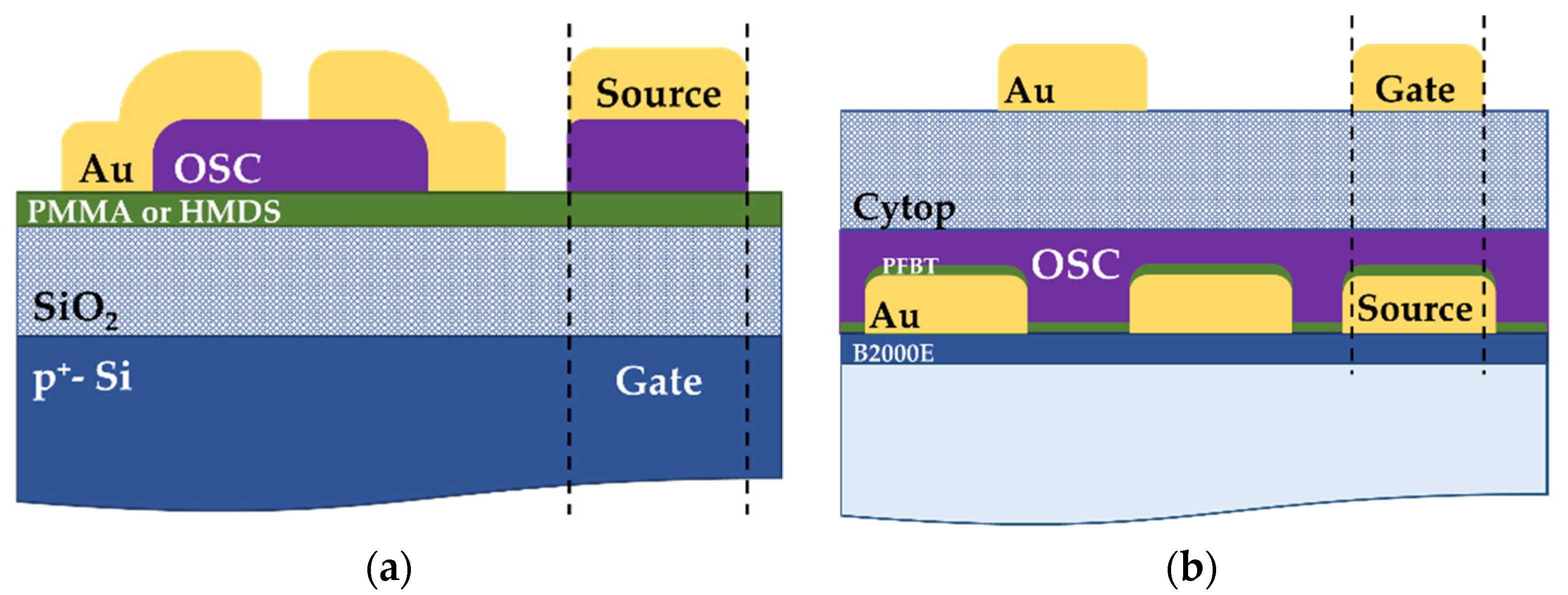
OTFTs were built in two architectures: bottom-gate/top-contact (BG/TC) and top-gate/bottom-contact (TG/BC). The semiconductor, processed by thermal evaporation, was the organic molecule C6-NTTN, where the intermediate π-unit contained thienothiophene, and the terminal π-units contained alkyl-substituted naphthalene [20].
The BG/TC devices (Figure 1a) were built on a p-Si substrate, acting as the bottom gate contact, covered by silicon dioxide (SiO2) with a thickness of 300 nm, acting as the gate dielectric. In order to analyze the effect of the dielectric surface energy, aside from the bare substrate, other gate insulators were obtained by covering the silicon oxide with a spin-coated thin film (15 nm thick) of poly(methyl methacrylate) (PMMA) or a self-assembled monolayer (SAM) of hexamethyldisilazane (HMDS). The organic semiconductor (OSC) was then evaporated, yielding a 60-nm thick film. In order to analyze the effect of the temperature at which the substrate was maintained during the semiconductor deposition, two high temperatures were employed for the HMDS-treated devices aside from room temperature (RT): 90 °C and 120 °C. On the top, the Au source and drain electrodes were evaporated with a thickness of 50 nm and an aspect ratio of 10 using a shadow mask.
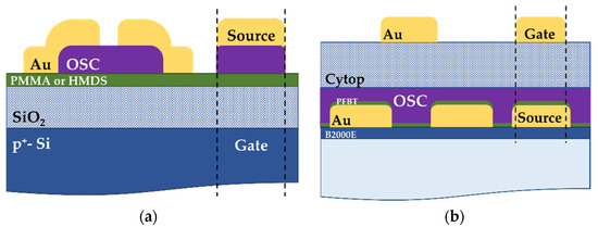
Figure 1.
Cross-sections of the fabricated OTFTs and, bounded by the dashed lines, the equivalent MIS capacitors in (a) BG/TC configuration and (b) TG/BC configuration.
The TG/BC devices (Figure 1b) were built on a glass substrate covered by a Polyera ActivInk® B2000E buffer polymer layer. The gold contacts were evaporated with a thickness of 50 nm. In order to study the effect of contact modification, aside from bare gold contacts, the SAM pentafluorobenzenethiol (PFBT) was spin-coated onto the substrate, thus changing both the substrate surface energy (hydrophobicity increased) and the metal work function (from 5.1 eV of gold to 5.35 eV) [21]. Then, the OSC was deposited by thermal evaporation at room temperature, affording a thickness of about 50 nm. The insulator layer was deposited by spin-coating Cytop at 3000 rpm for 60 s and subsequently annealing it at 100 °C, obtaining a thickness of 390 nm. Finally, a gold gate electrode was evaporated.
For each sample, the equivalent metal–insulator–semiconductor (MIS) capacitor was fabricated on the same substrate by depositing a single contact, referred to as the source, superimposed on the gate contact (Figure 1).
All measurements were developed at room temperature in ambient air. OTFT transfer curves were collected at VGS between −60 V and 20 V, and characteristic electrical parameters, such as the field effect mobility µFE, threshold voltage VTH, and subthreshold swing SS, were estimated by averaging the results of 6 devices for each configuration, using the following channel current equation in the saturation regime:
where W and L are the channel width and length, respectively, Ci is the dielectric capacitance, and VGS is the gate source voltage. VTH and µFE were evaluated as the VGS-axis intersection and from the slope of the tangent to (IDS)1/2, respectively.
The complex admittance of the MIS capacitors was measured using an Agilent E4980A LCR meter by superimposing a small signal of 10 mV to the DC bias. VGS was swept from −40 V to 20 V, while the small signal frequency was between 200 Hz and 2 MHz. The admittance Y(ω) was studied according to the parallel model through the capacitance CP and the loss LP (the loss is the conductance GP divided by the angular frequency ω and takes account of the energy dissipated by the device) and is expressed as follows:
The dielectric capacitance was extracted by measuring the equivalent metal–insulator–metal (MIM) device fabricated on each substrate. The bare, PMMA-, and HMDS-treated SiO2 had capacitances of 11.5, 9.5, and 11.2 nF/cm2, respectively, whereas the Cytop film’s was 4.7 nF/cm2.
The most meaningful results obtained from the electrical characterizations are discussed in relation to the semiconductor morphology obtained through AFM.
3. Results
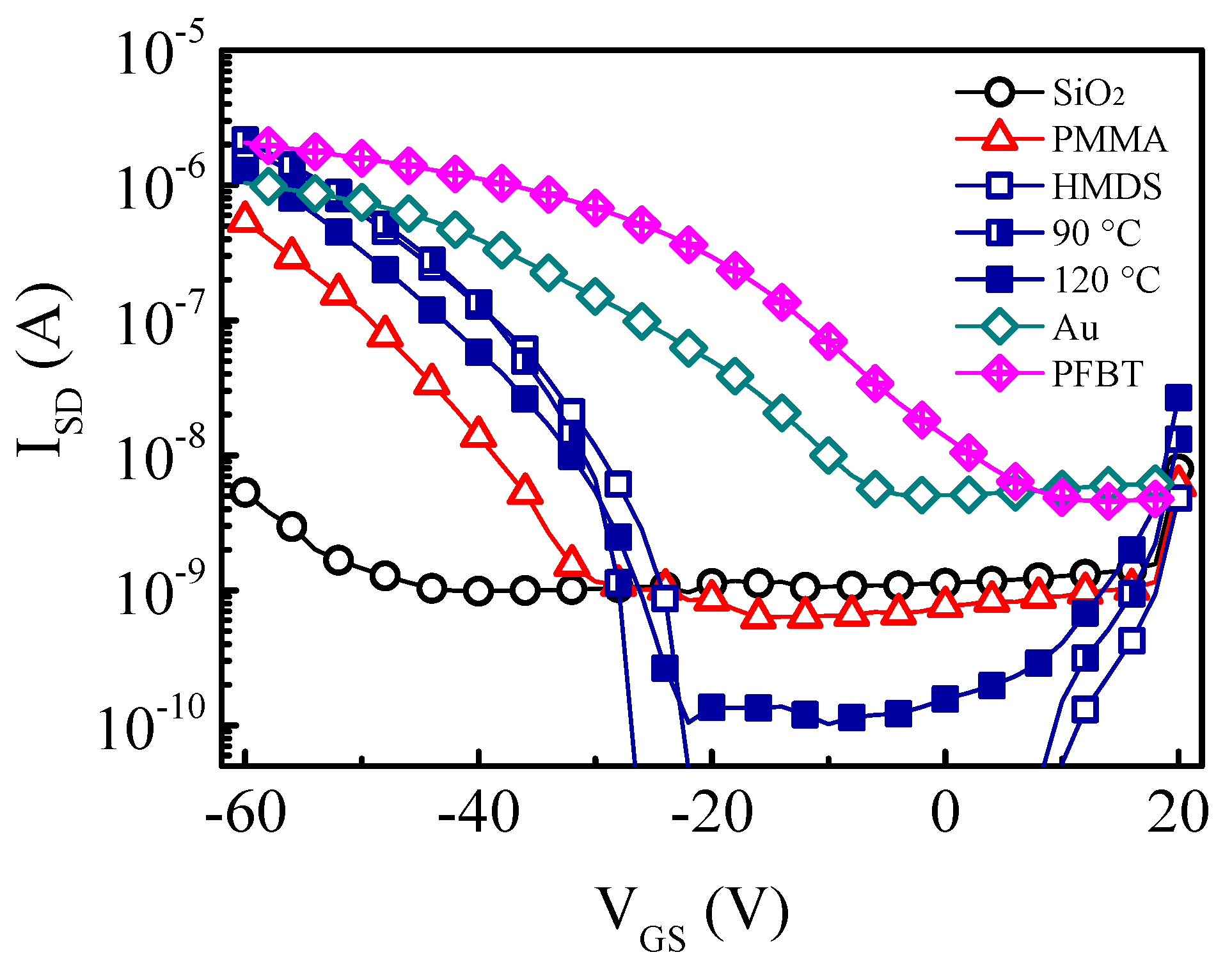
The representative transcharacteristics of the seven fabricated OTFTs in the saturation regime are compared in Figure 2. All devices were p-channel transistors with long-term stable characteristics. Observing the results obtained in the BG/TC configuration with an RT deposition, the worst features were detected in the bare SiO2-based OTFT, with a mobility of about 0.03 cm2/V·s and an average threshold voltage of −63 V. The insulator surface treatment improved the performance, with an increase in mobility to 0.09 and 0.11 cm2/V·s on the PMMA and HMDS, respectively, and a shift in VTH to −60 and −35 V, respectively.
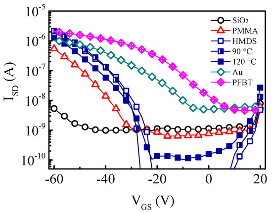
Figure 2.
Typical transcharacteristics of the fabricated OTFTs at VSD = 60 V. For the BG devices, open, half-solid, and solid symbols denote the semiconductor deposition at RT, 90 °C, and 120 °C, respectively, while the different colors indicate the various insulator interfaces (SiO2, PMMA, and HMDS). TG devices are denoted by diamond symbols, of which the cross-centered one indicates the Au contact functionalization (PFBT).
Regarding the effect of the substrate temperature, an increase in mobility up to a maximum of 0.16 cm2/V·s at 90 °C and a worsening at 120 °C, with an average value of 0.1 cm2/V·s, were observed. The threshold voltage, on the other hand, did not exhibit an evident relationship with the temperature, thus proven to result from the combination of multiple effects. The subthreshold swing showed the same trends of mobility in all the previous cases, demonstrating the existence of a strong relationship between the carrier mobility measured in the channel and the trap density at the interface with the insulator that could be extracted from SS [20].
Finally, regarding the results obtained for the samples in the top-gate configuration, the strongest effect due to PFBT treatment was observed in VTH, which translated from −11 V on bare substrate to about 0 on the treated contacts, while the increase in µFE from 0.02 to about 0.03 cm2/V·s was less significant. These variations could be attributed to the modification of both the metal work function and the substrate surface energy.
The admittance curves (reported in the discussion section) show some common features. First of all, the maximum value of the capacitance at a low frequency was measured in accumulation and was close to the insulator capacitor Ci. Moving toward the depletion regime, as the voltage varied, the overall capacitance decreased, since it corresponded to the series sum of Ci and the depletion capacitance CD.
On the other hand, as the frequency increased, three main dispersion events were observed, corresponding to a peak in the loss curve and a simultaneous reduction in capacitance. As can be easily seen from the appearance of the loss peaks, these dispersions had different properties and were representative of distinct phenomena. The first peak observed in the depletion regime at low frequencies moved with the bias but did not change significantly in amplitude, demonstrating the presence of traps in the channel area (i.e., near the semiconductor/insulator interface). The second peak shifted slightly in frequency while significantly decreasing in amplitude with bias, showing a correlation with the semiconductor bulk characterized by a dispersive transport. Finally, a third peak appeared at a high frequency and, being approximately constant both in frequency and in amplitude, it could be associated with a series resistance of the metal contact. Due to the overlap in frequency of these phenomena and their complex interaction, it is necessary to develop an appropriate model for correct data interpretation and the complete extraction of the device parameters.
4. Model
The model proposed for the data interpretation is an electrical circuit (Figure 3) whose elements describe the physical processes occurring in the various layers and at the different interfaces of the organic MIS device [18,19].
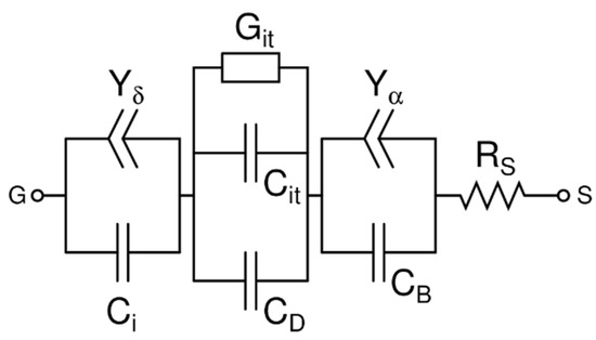
Figure 3.
Organic MIS capacitor equivalent circuit.
The gate insulator layer is defined by the parallel connection of the capacitor Ci = εi/ti, where εi and ti are its permittivity and thickness, respectively, and the constant phase element (CPE). The latter is expressed as:
It describes the anomalous diffusion of slow ions through the insulator [22], presumably water molecules, responsible for the forth weak dispersion occurring at very low frequency. Adiff depends on the diffusing particle density, and 0 < δ < 0.5 defines the continuous time random walk (δ = 0.5 corresponds to normal diffusion).
The semiconductor film, which is divided into a depleted layer and a bulk region whose widths vary with the bias, is described by the series combination of the depletion capacitor CD = εosc/wD, where εosc and wD are the OSC permittivity and depletion width, respectively, and the bulk capacitor CB = εosc/(tosc − wD), where tosc is the OSC thickness.
The effect of trapping at the semiconductor/insulator interface, generating the first main loss peak at a low frequency, is represented by the combination of the capacitor Cit and the conductance Git in parallel to CD, giving the following expression for the depletion layer admittance [23]:
where the presence of a continuous distribution of states with density Dit and relaxation time constant τit is assumed. The structural disorder of the OSC bulk, the cause of the dispersive transport, is described by a CPE in the form Yα = GB(jωτB)α, placed in parallel with CB to provide the following bulk admittance according to the Cole–Cole theory [24]:
where 0 < α < 1 is the dispersion parameter and τB is the OSC relaxation time. It imposes an upper limit on the frequency up to which the injected holes are able to follow the applied AC signal and therefore is responsible for the second main loss peak.
The back contact is, finally, represented by the series resistance RS, which describes the quality of the semiconductor/metal interface and is responsible for the loss peak at a high frequency.
The model equations were simulated for the seven devices in order to reproduce the experimental data of the complex admittance. While the capacitances of the insulator and OSC layers, in addition to all the known physical and geometrical parameters, were kept constant, all the other parameters were extracted by fitting the simulated curves with the experimental data. A good fit with an average R2 value of 0.999 was obtained.
Fundamental information, such as the onset voltage VON, the semiconductor doping density NA, and the surface potential φS, were obtained from the dependence of the depletion layer width wD, extracted from CD, on the bias using the following equations:
where ET is the interface trap level accessible at a band bending φS and EF is the bulk Fermi level.
5. Discussion
The results obtained by admittance spectroscopy are reported and discussed below, with the aim of correlating the process parameters with the electrical performance. In particular, the effects on the electrical characteristics of the treatment of the insulator surface, of the substrate temperature during semiconductor deposition, and of the metal contact modification are discussed. In addition, the differences between the two device architectures are analyzed. AFM images are reported to support discussion when significant differences have been detected.
5.1. Effect of Insulator Surface Treatment
The admittance curves of the devices deposited at RT on different insulators are reported in Figure 4, and the extracted parameters are in Table 1. In the comparison between the bare and treated silicon oxide, a significant parameter was Adiff. While δ was equal to about 0.2 for all insulating films, indicating an anomalous diffusion, Adiff had lower values in the presence of PMMA and HMDS, showing their effectiveness in counteracting the absorption of water and the diffusion of mobile ions through the insulator by forming a barrier. The methyl methacryl groups of PMMA and the methyl groups of HMDS formed a hydrophobic surface, which on the one hand improved the growth of the OSC film, as shown by the increased mobility in the channel, and on the other hand blocked the charge injection from the channel, as shown by the reduction in OTFT leakage currents.
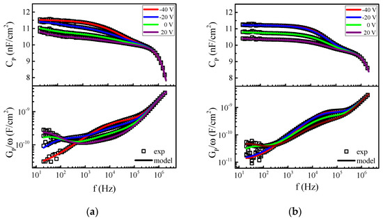
Figure 4.
Admittance curves of MIS devices with semiconductor deposited at RT on (a) SiO2 and (b) SiO2/HMDS. Model curves (solid lines) are superimposed on the experimental data (squared symbols).

Table 1.
Model parameters extracted for OTFTs in BG configuration on different insulator layers.
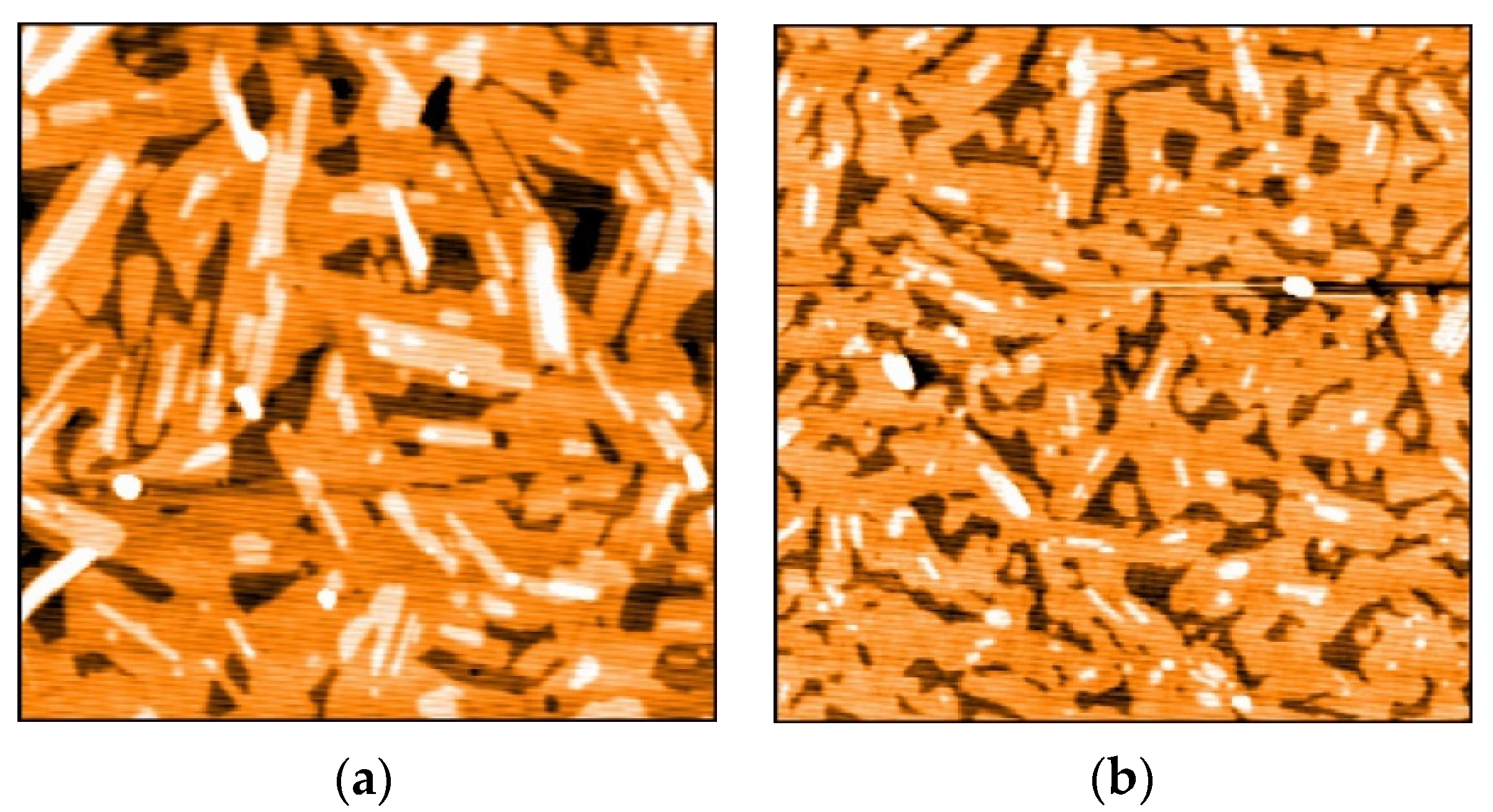
In addition, the doping density NA, lower for the PMMA and even more for the HMDS, demonstrated an improvement in the OSC morphology which, as reported in Figure 5, became more homogeneous and interconnected thanks to the more hydrophobic substrate.
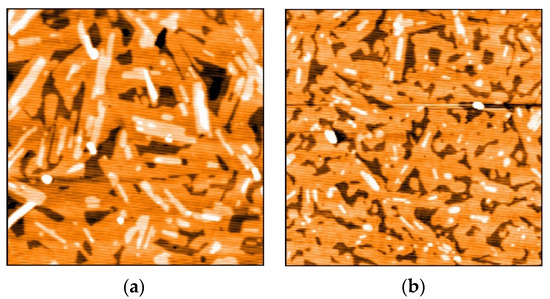
Figure 5.
AFM images (5 µm × 5 µm) of OSC film deposited at RT (a) on SiO2 and (b) on SiO2/HMDS.
The lower values of ρOSC and α for the treated substrates show that the properties of the bulk semiconductor were improved, while the values of Dit demonstrate a reduction of the traps which, located at the interface with the insulator, limited the charge transport. An inverse proportionality between Dit and µFET was observed.
5.2. Effect of the Substate Temperature
The admittance curves of the devices with semiconductors deposited on HMDS at higher temperatures are reported in Figure 6. The parameters extracted through the model (Table 2) show that the main effect of the increase in substrate temperature during deposition was improvement of the OSC conductivity, with a reduction in both the interface traps and bulk dispersion, while an excessive increase in temperature led to a deterioration in performance.
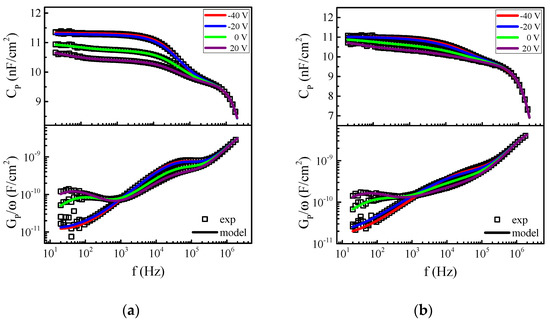
Figure 6.
Admittance curves of MIS devices with semiconductor deposited on SiO2/HMDS at (a) 90 °C and (b) 120 °C. Model curves (solid lines) are superimposed on the experimental data (squared symbols).
Table 2.
Model parameters extracted for OTFTs in BG configuration on SiO2/HMDS insulator for different substrate temperatures during OSC deposition.
The AFM images of the semiconductor film collected on HMDS show that the increase of the substrate temperature induced the creation of wider grains (Figure 7) thanks to the enhanced molecular diffusion on the substrate surface allowing a layer-by-layer film growth [25]. This phenomenon justifies the mobility improvement and confirms the reduction in the trap density at 90 °C. However, the temperature increase made the growing aggregates less interconnected. Indeed, for the semiconductor deposited at 120 °C, wide gaps separated the polycrystalline domains, according to the higher trap density responsible for the reduction in mobility µFE.
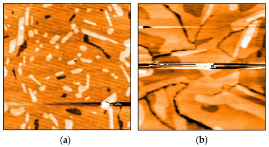
Figure 7.
AFM images (5 µm × 5 µm) of OSC film deposited SiO2/HMDS at (a) 90 °C and (b) 120 °C.
5.3. Effect of Contact Modification
Admittance experimental data and model curves comparing devices in the TG/BC configuration with bare and treated contacts are shown in Figure 8. The model parameters, reported in Table 3, demonstrate that the improvement in the OTFT threshold voltage, which was a fitting parameter derived from the MOSFET theory valid for the operation with channel inversion, could actually be explained as the translation of the onset voltage, which was instead associated with the flat band condition and directly depended on the channel area and contact properties. In this case, when comparing the VON and RS values, it is evident that the reduction in the onset voltage was due to a significant decrease in the contact resistance. The AFM images showed no significant difference in the semiconductor morphology, confirming that the PFBT treatment mainly modified the contacts. Due to the increase in the Au function, a flow of electrons coming from the semiconductor was established toward the metal and up to its Fermi level pinning, causing p-type OSC doping at the metal interface [26] and onset voltage shift to the right [27].
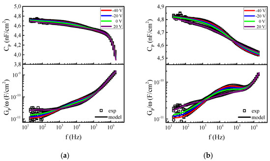
Figure 8.
Admittance curves of MIS devices with (a) bare Au contacts and (b) PFBT-treated contacts. Model curves (solid lines) are superimposed on the experimental data (squared symbols).
Table 3.
Model parameters extracted for OTFTs in TG configuration with different contacts.
5.4. Effect of the Device Architecture
The BG/TC device configuration had the advantage of allowing access to the surface of the gate insulator in order to perform treatments before the semiconductor deposition and directly improve the channel area, while the TG/BC geometry also allowed electrode modification before the OSC deposition and was appreciable for the superior position of the dielectric, which also acted as a barrier to the environment.
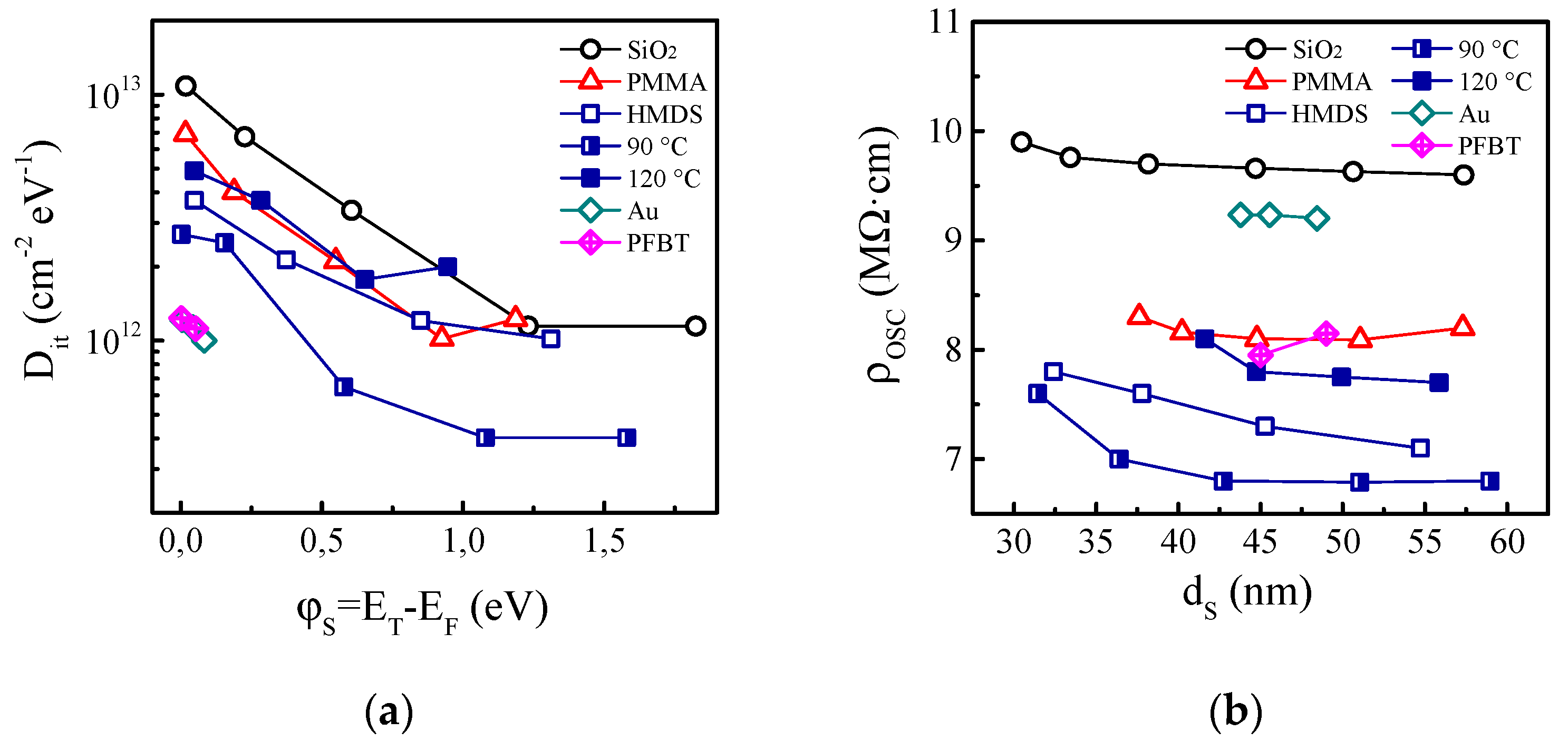
A fundamental parameter of comparison between the two architectures is the interface trap density. The values of Dit, which were extracted from Cit and Git and reported in Figure 9a as a function of the surface potential φS, showed the presence of an approximately exponential distribution. Furthermore, from the comparison between the two architectures, it is evident that the interface created between the semiconductor and the Cytop insulator in the TG configuration was better than that formed with bare or treated silicon oxide in the BG configuration. Despite this, the resulting channel mobility and the bulk conductivity (Figure 9b) in the TG/BC devices was lower than the other case, and it was not significantly improved through the treatment of the lower surface (i.e., the metal contact). The latter, in fact, could induce a strong variation only in a solution-deposited film, where the surface roughness reduced, or in the first layers of a thermally evaporated semiconductor [18,28].
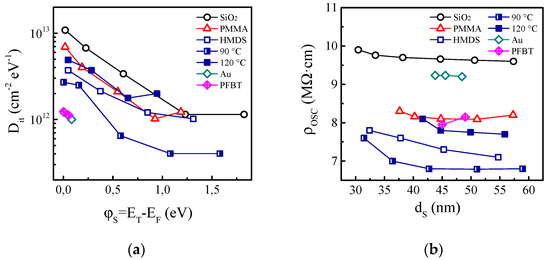
Figure 9.
(a) Interface density of states as a function of surface potential and (b) average resistivity of the OSC bulk of thickness ds next to source contact. For BG devices, open, half-solid, and solid symbols denote the semiconductor deposition at RT, 90 °C, and 120 °C, respectively, while the different colors indicate the various insulator interfaces (SiO2, PMMA, and HMDS). TG devices are denoted by diamond symbols, of which the cross-centered one indicates the Au contact functionalization (PFBT).
The results obtained from the admittance analysis show that various factors contributed to the reduction of the threshold voltage. Among these was the OSC film morphology, due to the molecule nucleation process, which was affected by the substrate surface energy. The model parameters, and in particular the dispersion parameter values of the organic semiconductor in both configurations, demonstrate that a hydrophobic substrate was preferable because, as observed in the BG devices with PMMA and HMDS treatments and in the TG devices with PFBT treatment, it reduced the structural defects [29].
The further improvement in VTH observed in the TG/BC devices could be attributed to two other elements. One is the stability of Cytop, as demonstrated by its reduced diffusion factor Adiff. Cytop is indeed an insulator rich in fluorine and free of hydroxyl groups, aspects that make it water-repellent and an effective barrier to the environment [30] with a consequent reduction in interface trapping, as confirmed by the lower trap density revealed in the TG devices. The other one is the increase in the work function of gold for the effect of the thiol. Admittance spectroscopy showed that the contact resistance reduced thanks to the metal modification.
6. Conclusions
An electrical model was proposed to extract the significant parameters of OTFTs, characterized through admittance spectroscopy, with the aim of understanding the physical phenomena underlying the device operation and the relationship between the fabrication processes and the electrical performance. This is particularly useful in the case of devices based on novel materials and for the comparison of different treatments.
Author Contributions
Conceptualization, R.L., A.F., G.D.L. and L.D.B.; formal analysis, R.L.; investigation, R.L.; resources, A.F. and G.D.L.; data curation, R.L. and L.D.B.; writing—original draft preparation, R.L.; writing—review and editing, R.L., A.F., G.D.L. and L.D.B. All authors have read and agreed to the published version of the manuscript.
Funding
This research received no external funding.
Conflicts of Interest
The authors declare no conflict of interest.
References
- Xu, Y.; Liu, W.; Huang, Y.; Jin, C.; Zhou, B.; Sun, J.; Yang, J. Recent advances in flexible organic synaptic transistors. Adv. Electron. Mater. 2021, 7, 2100336. [Google Scholar] [CrossRef]
- Hadiyanto, M.Y.; Estrada, R.; Lee, C.C.; Biring, S.; Akbar, A.K.; Li, C.Y.; Shih, C.J.; Li, Y.Z.; Liu, S.W. Transparent photodetectors with ultra-low dark current and high photoresponse for near-infrared detection. Org. Electron. 2021, 99, 106356. [Google Scholar] [CrossRef]
- Botta, A.; Costabile, C.; Venditto, V.; Pragliola, S.; Liguori, R.; Rubino, A.; Alberga, D.; Savarese, M.; Adamo, C. Optoelectronic properties of poly(N-alkenyl-carbazole)s driven by polymer stereoregularity. J. Polym. Sci. Pol. Chem. 2018, 56, 242–251. [Google Scholar] [CrossRef]
- Liguori, R.; Botta, A.; Rubino, A.; Pragliola, S.; Venditto, V. Stereoregular polymers with pendant carbazolyl groups: Synthesis, properties and optoelectronic applications. Synth. Met. 2018, 246, 185–194. [Google Scholar] [CrossRef]
- Fusco, S.; Maglione, C.; Velardo, A.; Piccialli, V.; Liguori, R.; Peluso, A.; Rubino, A.; Centore, R. N-Rich Fused Heterocyclic Systems: Synthesis, Structure, Optical and Electrochemical Characterization. Eur. J. Org. Chem. 2016, 2016, 1772–1780. [Google Scholar] [CrossRef]
- Mittal, P.; Yadav, S.; Negi, S. Advancements for organic thin film transistors: Structures, materials, performance parameters, influencing factors, models, fabrication, reliability and applications. Mat. Sci. Semicond. Proc. 2021, 133, 105975. [Google Scholar] [CrossRef]
- Liguori, R.; Botta, A.; Pragliola, S.; Rubino, A.; Venditto, V.; Velardo, A.; Aprano, S.; Maglione, M.G.; Prontera, C.T.; Mauro, A.D.G.D.; et al. Study of the electroluminescence of highly stereoregular poly(N-pentenyl-carbazole) for blue and white OLEDs. Semicond. Sci. Technol. 2017, 32, 065006. [Google Scholar] [CrossRef]
- Dadhich, S.; Dwivedi, A.D.D.; Singh, A.K. Fabrication, characterization, numerical simulation and compact modeling of P3HT based organic thin film transistors. J. Semicond. 2021, 42, 074102. [Google Scholar] [CrossRef]
- Falco, A.; Nagel, R.; Lugli, P.; Bezzeccheri, E.; Liguori, R.; Rubino, A. Simulation and fabrication of polarized organic photodiodes. In Proceedings of the IEEE Sensors, Orlando, FL, USA, 30 October–3 November 2016; p. 7808585. [Google Scholar]
- Liguori, R.; Rubino, A. Metastable light induced effects in pentacene. Org. Electron. 2014, 15, 1928–1935. [Google Scholar] [CrossRef]
- Wisniewski, P.; Jasinski, J.; Mazurak, A.; Stonio, B.; Majkusiak, B. Investigation of electrical properties of the Al/SiO2/n++-Si resistive switching structures by means of static, admittance, and impedance spectroscopy measurements. Materials 2021, 14, 6042. [Google Scholar] [CrossRef]
- Arnal, A.; Crespo-Yepes, A.; Ramon, E.; Teres, L.; Rodriguez, R.; Nafria, M. DC characterization and fast small-signal parameter extraction of organic thin film transistors with different geometries. IEEE Electron Dev. Lett. 2020, 41, 1512–1515. [Google Scholar] [CrossRef]
- Manda, P.K.; Karunakaran, L.; Dutta, S. Modeling the frequency response of organic metal-insulator-semiconductor capacitors. Mater. Today Proc. 2019, 19, 53–57. [Google Scholar] [CrossRef]
- Bezzeccheri, E.; Femia, A.; Liguori, R.; Rubino, A. Interface trap state characterization of metal-insulator-semiconductor structures based on photosensitive organic materials. Mater. Today Proc. 2017, 4, 5045–5052. [Google Scholar] [CrossRef]
- Fiorillo, M.; Liguori, R.; Diletto, C.; Bezzeccheri, E.; Tassini, P.; Maglione, M.; Maddalena, P.; Minarini, C.; Rubino, A. Analysis of HMDS self-assembled monolayer effect on trap density in PC70BM n-type thin film transistors through admittance studies. Mater. Today Proc. 2017, 4, 5053–5059. [Google Scholar] [CrossRef]
- Hirwa, H.; Pittner, S.; Wagner, V. Interface analysis by impedance spectroscopy and transient current spectroscopy on semiconducting polymers based metal-insulator-semiconductor capacitors. Org. Electron. 2015, 24, 303–314. [Google Scholar] [CrossRef]
- Marin, A.T.; Musselman, K.P.; MacManus-Driscoll, J.L. Accurate determination of interface trap state parameters by admittance spectroscopy in the presence of a Schottky barrier contact: Application to ZnO-based solar cells. J. Appl. Phys. 2013, 113, 144502. [Google Scholar] [CrossRef] [Green Version]
- Liguori, R.; Rubino, A. Admittance spectroscopy and material modeling for organic electronic applications. Mater. Today Proc. 2021, 44, 2033–2037. [Google Scholar] [CrossRef]
- Liguori, R.; Licciardo, G.D.; Di Benedetto, L. Organic transistor parameter estimation and accurate modeling for process optimization. In Proceedings of the SMACD/PRIME 2021; International Conference on SMACD and 16th Conference on PRIME, online, 19–22 July 2021; pp. 228–231. [Google Scholar]
- Liguori, R.; Usta, H.; Fusco, S.; Facchetti, A.; Licciardo, G.D.; Di Benedetto, L.; Rubino, A. Insight into interface treatments in p-channel organic thin film transistors based on a novel molecular semiconductor. IEEE Trans. Electron Dev. 2017, 64, 2338–2344. [Google Scholar] [CrossRef]
- Fenwick, O.; Van Dyck, C.; Murugavel, K.; Cornil, D.; Reinders, F.; Haar, S.; Mayor, M.; Cornil, J.; Samorì, P. Modulating the charge injection in organic field-effect transistors: Fluorinated oligophenyl self- assembled monolayers for high function electrodes. J. Mater. Chem. C 2015, 3, 3007–3015. [Google Scholar] [CrossRef] [Green Version]
- Ledru, R.; Pleutin, S.; Grouiez, B.; Zander, D.; Bejbouji, H.; Lmimouni, K.; Vuillaume, D. Low frequency dielectric loss of metal/insulator/organic semiconductor junctions in ambient conditions. Org. Electron. 2012, 13, 1916–1924. [Google Scholar] [CrossRef] [Green Version]
- Li, J.; Chen, Z.; Qu, Y.; Zhang, R. Traps around Ge Schottky junction interface: Quantitative characterization and impact on the electrical properties of Ge MOS Devices. IEEE J. Electron Devices Soc. 2020, 8, 350–357. [Google Scholar] [CrossRef]
- Drewniak, L.; Kochowski, S. The origin of constant phase element in equivalent circuit of MIS (n) GaAs structures. J. Mater. Sci. Mater. Electron. 2020, 31, 19106–19118. [Google Scholar] [CrossRef]
- Shur, M.; Fjeldly, T.A.; Ytterdal, T.; Lee, K. Unified MOSFET model. Solid State Electron. 1992, 35, 1795–1802. [Google Scholar] [CrossRef]
- Rolland, A.; Richard, J.; Kleider, J.P.; Mencaraglia, D. Electrical properties of amorphous silicon transistors and MIS-devices: Comparative study of top nitride and bottom nitride configurations. J. Electrochem. Soc. 1993, 140, 3679–3683. [Google Scholar] [CrossRef]
- Kim, C.; Facchetti, A.; Marks, T.J. Probing the surface glass transition temperature of polymer films via organic semiconductor growth mode, microstructure, and thin-film transistor response. J. Am. Chem. Soc. 2009, 131, 9122–9132. [Google Scholar] [CrossRef]
- Gundlach, D.J.; Royer, J.E.; Park, S.K.; Subramanian, S.; Jurchescu, O.D.; Hamadani, B.H.; Moad, A.J.; Kline, R.; Teague, L.C.; Kirillov, O.; et al. Contact-induced crystallinity for high-performance soluble acene-based transistors and circuits. Nat. Mater. 2008, 7, 216–221. [Google Scholar] [CrossRef]
- Celle, C.; Suspène, C.; Ternisien, M.; Lenfant, S.; Guerin, D.; Smaali, K.; Lmimouni, K.; Simonato, J.-P.; Vuillaume, D. Interface dipole: Effects on threshold voltage and mobility for both amorphous and poly-crystalline organic field effect transistors. Org. Electron. 2014, 15, 729–737. [Google Scholar] [CrossRef] [Green Version]
- Walser, M.P.; Kalb, W.L.; Mathis, T.; Batlogg, B. Low-voltage organic transistors and inverters with ultrathin fluoropolymer gate dielectric. Appl. Phys. Lett. 2009, 95, 233301. [Google Scholar] [CrossRef] [Green Version]


Publisher’s Note: MDPI stays neutral with regard to jurisdictional claims in published maps and institutional affiliations. |
© 2022 by the authors. Licensee MDPI, Basel, Switzerland. This article is an open access article distributed under the terms and conditions of the Creative Commons Attribution (CC BY) license (https://creativecommons.org/licenses/by/4.0/).