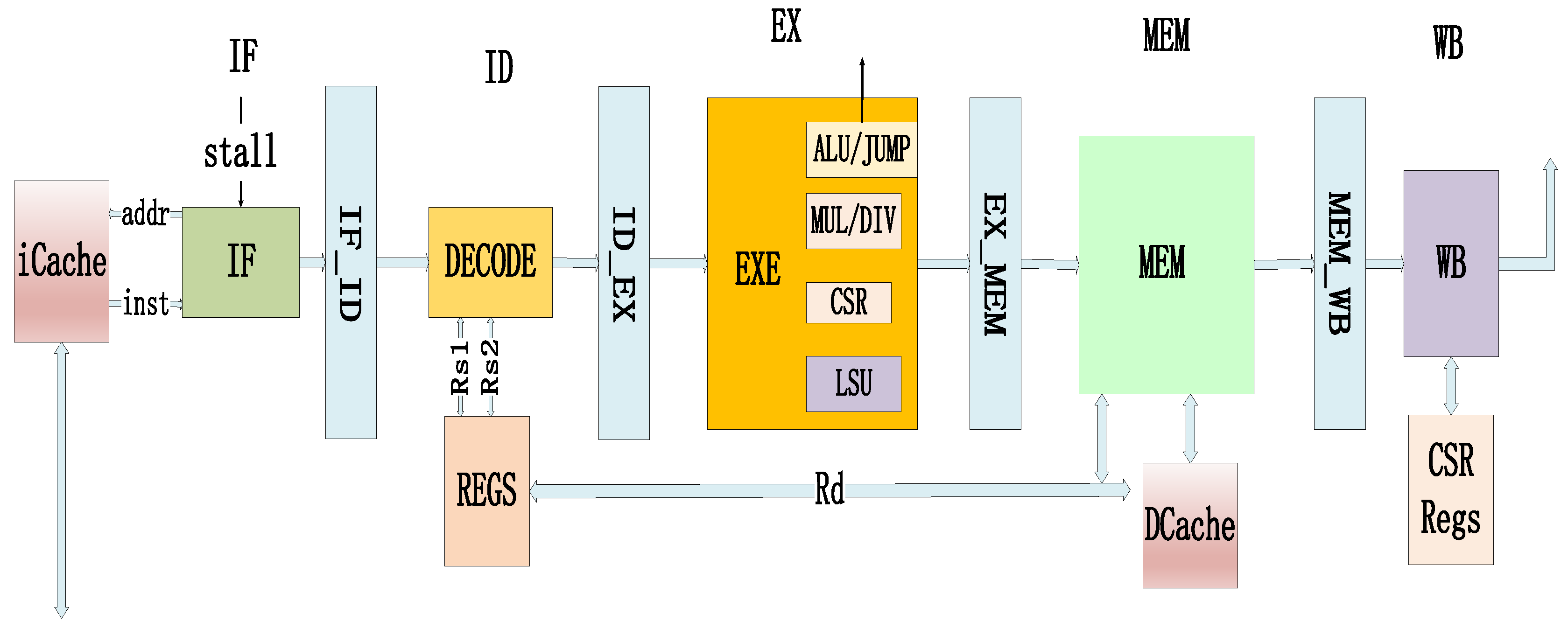
Article

DuckCore: A Fault-Tolerant Processor Core Architecture Based on the RISC-V ISA

1
Technology and Engineering Center for Space Utilization, Chinese Academy of Sciences, Beijing 100094, China
2
Key Laboratory of Space Utilization, Chinese Academy of Sciences, Beijing 100094, China
3
University of Chinese Academy of Sciences, Beijing 100049, China
*
Author to whom correspondence should be addressed.
Electronics 2022, 11(1), 122; https://doi.org/10.3390/electronics11010122
Submission received: 31 October 2021 / Revised: 19 December 2021 / Accepted: 22 December 2021 / Published: 30 December 2021

Abstract

:
With the development of large-scale CMOS-integrated circuit manufacturing technology, microprocessor chips are more vulnerable to soft errors and radiation interference, resulting in reduced reliability. Core reliability is an important element of the microprocessor’s ability to resist soft errors. This paper proposes DuckCore, a fault-tolerant processor core architecture based on the free and open instruction set architecture (ISA) RISC-V. This architecture uses improved SECDED (single error correction, double error detection) code between pipelines, detects processor operating errors in real-time through the Supervision unit, and takes instruction rollbacks for different error types, which not only saves resources but also improves the reliability of the processor core. In the implementation process, all error injection tests are passed to verify the completeness of the function. In order to better verify the performance of the processor under different error intensity injections, the software is used to inject errors, the running program is run on the FPGA (Field Programmable Gate Array), and the impact of the actual radiation environment on the architecture is evaluated through the results. The architecture is applied to three–five-stage open-source processor cores and the results show that this method consumes fewer resources and its discrete design makes it more portable.

1. Introduction

The free and open RISC-V instruction set architecture (ISA) has the characteristics of modularity, low power consumption, high performance, and easy expansion. It has attracted an active community building processor cores and ecosystems, which makes it competitive to established processor designs [1]. A large number of open-source processor cores have appeared in commercial and academic circles within a few years [2]. Even so, there are still not many processor architectures with high reliability and high fault tolerance [3]. Most of the radiation-resistant processors commonly used in space applications are based on SPARCV8, ARM, and MIPS architectures. The characteristics of the RISC-V architecture have a large application range in space electronic equipment.
Soft errors are transient faults caused by noise interference or the impact of high-energy particles. With the development of integrated circuit manufacturing technology (Moore’s Law), soft errors caused by radiation and interference are increasing, which results in the problem of reduced reliability, which will limit the development and application of modern advanced microprocessors [4]. For processors in a space environment, the radiation problems encountered are even more severe, especially single event effects (SEEs), such as single event upset (SEU) and single event latching (SEL) [5]. Studies [6] have shown that 80% to 90% of failures in computer systems are caused by transient faults. Therefore, it is of great significance to solve the problem of soft errors and improve the fault tolerance of the processor so that it can be better applied to various complex and changeable environments.
The fault tolerance of the processor core depends on its design architecture, and commercial processor cores are often in a black box state, which makes it difficult to harden the fault tolerance [7]. The fault tolerance for storage space often uses Hamming code or ECC check technology [8,9], but Hamming code can only correct 1-bit errors, not multi-bit errors. The trigger design [10] based on Triple Modular Redundancy (TMR) technology can effectively improve fault tolerance, however, it uses many more resources. Checkpoint-oriented recovery methods have the ability to cover errors using rollback, but they often face the problem of setting checkpoint locations [11]. The results of previous research [12,13] show that the design for software redundancy can be reinforced without relying on the hardware itself, but additional inspection instructions need to be added to this function. The fault-tolerant design [14,15] using commercial processor cores mostly uses a multi-core design to improve the safety of its system, but a multi-core design will consume a lot of resources.
In this paper, we aim to combine a variety of strategies to improve the fault tolerance of the processor core, so that it can adapt to the complex radiation environment while having good performance and a low resource ratio. We combined improved SECDED code, error supervision, pipeline rollback, and other technologies, and proposed the DuckCore fault-tolerant architecture. The DuckCore architecture is verified on FPGA and has ideal error correction ability. This scheme is also applied to some open-source [16,17,18] processor cores to compare and analyze resource usage. In addition, it can be easily applied to the processor architecture of a two–five-stage in-order microprocessor, and achieve a good balance between reliability and performance.
The remainder of this paper follows the ensuing structure: in Section 2, the related works of our predecessors are introduced, the fault-tolerant design methods and ideas of each processor are analyzed, and their respective advantages and disadvantages are clarified as well. In Section 3, the design ideas and methods of DuckCore are introduced. In Section 3.1, a general five-stage sequential pipeline architecture model based on the RISC-V instruction set is given. In Section 3.2, the design of the improved SECDED code is introduced. In Section 3.3, the design of the pipeline inspection and rollback strategy is presented in detail. In Section 3.4, the operation mechanism and processing method are illustrated with examples. In Section 4, the verification scheme of this architecture and the software and hardware test platform are given. In Section 5, the results of the functional test are given, the impact of processor performance under different error types is compared, and the application resource occupation of the architecture is analyzed. Finally, in Section 6, the conclusions are recapitulated.

2. Related Work

Integrated circuit technology and architecture technology have jointly promoted the development of microprocessors. At the same time, the advancement of these two technologies has also introduced new challenges and opportunities into the soft and error-tolerant design of microprocessors. The methods commonly used by fault-tolerant processors mainly include spatial redundancy, temporal redundancy, and information redundancy [19]. Spatial redundancy involves TMR and multi-core technology, while time fault tolerance is mainly based on multithreading technology. Redundant multithreading (RMT) for SMT (simultaneous multithreading) processors [20,21] is a good way to achieve fault tolerance. Information redundancy is mainly implemented by means of error correction such as coding.
EDAC (Error Detecting and Correcting Code) can be used to detect and correct errors in microprocessors caused by SEU. It is a common technology used in digital communications to improve the reliability of data transmission. For example, the highly reliable 8051 microprocessor of the French TIMA laboratory [22] uses the Hamming code method to protect its internal memory and data. The use of Hamming code for fault-tolerant reinforcement brings more resource consumption as the number of source codes and digits increases. Many scholars have proposed improved Hamming codes. U. K. Kumar et al. [23] change the order of check bits to implement an improved Hamming code, which reduces circuit consumption and saves more resources in the face of large-scale storage devices.
Early fault-tolerant processors are mostly based on architectures such as SPARCV8, 8051, and RISC. Chris Weaver et al. [24] used a parallel pipeline inspection core to monitor the running status of the processor and rollback errors in real-time, which improves fault tolerance. However, inspections require more resources. Jiri Gaisler et al. [25] designed a LEON-F microprocessor based on the SPARCV8 architecture. The processor adopts a dual-core mutual supervision architecture, the internal trigger of each single-core adopts a TMR design, and the memory uses BCH (Bose–Chaudhuri–Hocquenghem) code to achieve error detection and correction. The processor also has strong fault tolerance, and the encoding and dual-core methods take up more resources. Todd M. Austin et al. [26] proposed the DIVA architecture to implement error-checking technology for multi-stage pipeline processor cores. Abdelmajid Bouajila et al. [27] made changes to the DIVA technology to improve the reliability of the check core itself and applied the improved DIVA technology to the seven-stage pipeline core LEON3. Both methods deal with errors in the write-back stage, which brings performance loss in the face of a more complex radiation environment.
With the development of RISC-V, a large number of open-source processor cores have appeared in academic and commercial markets [28]. In recent years, the RISC-V processor has also been deeply studied and applied in the Internet of Things, neural networks, artificial intelligence, and so on [29,30,31,32]. There are not many RISC-V processors with fault-tolerant architecture currently publicly available. The SHAKTI-F processor core [8], open-sourced by the Indian Institute of Technology, based on the RV32I architecture, adds SECDED code between each stage of the pipeline and uses repetitive computing technology to solve the double-bit error problem. However, SHAKTI-F only considers inspections in the execution stage, ignoring exceptions in other pipelines. Alexander et al. [9] focused on improving the fault tolerance of the RISC-V processor in the storage architecture. They designed the ECC module based on the characteristics of the Chisel language and successfully transplanted it to the rocket and other processor cores without considering the internal core reliability. Douglas Almeida Santos et al. designed a low-power three-stage pipelined RISC-V processor, using TMR technology on the arithmetic unit and 38-bit Hamming code verification on the fetch stage. This method is similar to SHAKTI-F, as it only considers the RV32I architecture and does not consider multi-bit errors and complex pipeline conditions [3]. Similarly, the authors of [33] used Hamming code combined with TMR technology and proposed a processor architecture based on RV32I. Cristiano Rodrigues et al. [34] designed a fault-tolerant architecture based on ARM and RISC-V dual-core redundancy, but this method is too resource-intensive. Mong Tee Sim et al. [15] used dual-core lockstep technology based on the RISC-V core to achieve fault-tolerance, and this method is suitable for fast error recovery in safety-critical applications.

3. Architecture Design

The DuckCore (this name was devised by our project team; in this paper, it refers to an architecture using a combination of coding and rollback technology) core architecture is designed for fault-tolerance on the classic five-stage in-order pipeline architecture. It adopts improved SECDED code and draws on the architectural concepts of SHAKTI-F and DIVA technology. It has the capability for real-time monitoring of instruction running status and error rollback, which can more effectively improve the processor’s anti-single event upset ability. This architecture can be applied to small microprocessor architectures with two–five-stage in-order pipelines.

3.1. Baseline Pipeline Structure

The classic architecture model of the DuckCore is based on the RV32IM instruction set, using a classic five-stage in-order pipeline design, as shown in Figure 1, including fetch (IF), decoding (DE), execution (EXE), memory access (MEM), write-back (WB) in five stages. The privileged instruction set of the RISC-V instruction set is realized through the CSR register and its internal control module.
Fetch (IF): The fetch module determines the next instruction that needs to enter the pipeline. If the pipeline is paused (due to data correlation or internal errors), it stops the instruction fetch. If the pipeline has a branch jump (interrupt or branch instruction), then the next fetch address becomes the jump address. Otherwise, the fetch module fetches instructions, increasing the address by four.
Decoding (DE): The decoding module decodes the instructions of the fetch module according to the RISC-V encoding format. A total of 58 RISC-V instructions are implemented in this design, and various instructions are classified and distinguished in the decoding stage.
Execution (EXE): The execution considers the realization of all instructions: arithmetic and logic operations, jump instruction processing, CSR instruction processing, multiplication and division operations, etc. In the execution stage, the memory address and register address required by the MEM stage are also calculated.
Memory access (MEM): The LOAD/STORE instructions and storage-related operations are implemented in the memory access stage.
Write-back (WB): The data to be written into the register is delayed for one cycle in the write-back stage. The register processor includes 32 general registers and CSR registers.
A simple five-stage pipeline model can be divided into combinational logic and sequential logic. The sequential logic part of the divided module is concentrated in the four modules of IF_ID, ID_EX, EX_MEM, and MEM_WB. Both the REGS module and the CSR REGS module are related to storage data access, and there are also sequential logic circuits. The combinational logic circuit module is also divided according to the module, and the model diagram is shown in Figure 2.
A simpler three-stage pipeline model is shown in Figure 3 below.

3.2. Improved SECDED Code

The SHAKTI-F processor core uses the classic SECDED code [35]. In this architecture, it is necessary to perform on-site recovery and code verification operations on the data. As the amount of data increases, this coding method is somewhat complex and does not save resources. Therefore, we made an improvement to the coding based on the method proposed by U. K. Kumar [23].
The classic 32-bit SECDED encoding requires seven parity bits according to the encoding rules of Hamming code. Consider the source code as the following data, define A1 as 32-bit source code data, and D X   or   P X as a single-bit number:
A 1 [ 31 : 0 ] = D 1 D 2 D 3 D 4 D 5 D 6 D 7 D 8 D 9 D 10 D 11 D 12 D 13 D 14 D 15 D 16 D 17 D 18 D 19 D 20 D 21 D 22 D 23 D 24 D 25 D 26 D 27 D 28 D 29 D 30 D 31 D 32
The data (define B1 as 39-bit data) after inserting the check bits becomes:
B 1 [ 38 : 0 ] = P 1 P 2 D 1 P 3 D 2 D 3 D 4 P 4 D 5 D 6 D 7 D 8 D 9 D 10 D 11 P 5 D 12 D 13 D 14 D 15 D 16 D 17 D 18 D 19 D 20 D 21 D 22 D 23 D 24 D 25 D 26 P 6 D 27 D 28 D 29 D 30 D 31 D 32 P 7
According to the coding rules of Hamming code, the check bits are calculated as follows:
P 1 = D 1 D 2 D 4 D 5 D 7 D 9 D 11 D 12 D 14 D 16 D 18 D 20 D 22 D 24 D 26 D 27 D 29 D 31
P 2 = D 1 D 3 D 4 D 6 D 7 D 10 D 11 D 13 D 14 D 17 D 18 D 21 D 22 D 25 D 26 D 28 D 29 D 32
P 3 = D 2 D 3 D 4 D 8 D 9 D 10 D 11 D 15 D 16 D 17 D 18 D 23 D 24 D 25 D 26 D 30 D 31 D 32
P 4 = D 5 D 6 D 7 D 8 D 9 D 10 D 11 D 19 D 20 D 21 D 22 D 23 D 24 D 25 D 26
P 5 = D 12 D 13 D 14 D 15 D 16 D 17 D 18 D 19 D 20 D 21 D 22 D 23 D 24 D 25 D 26
P 6 = D 27 D 28 D 29 D 30 D 31 D 32
P 7 = D 1 D 2 D 3 D 5 D 6 D 8 D 11 D 12 D 13 D 15 D 16 D 18 D 19 D 20 D 22 D 25 D 27 D 28 D 30 D 31 D 32
The decoding is based on the received 39-bit encoded data. Assume that the received data is:
B [ 38 : 0 ] = P 1 P 2 D 1 P 3 D 2 D 3 D 4 P 4 D 5 D 6 D 7 D 8 D 9 D 10 D 11 P 5 D 12 D 13 D 14 D 15 D 16 D 17 D 18 D 19 D 20 D 21 D 22 D 23 D 24 D 25 D 26 P 6 D 27 D 28 D 29 D 30 D 31 D 32 P 7
Then the decoding equations are:
S 1 = P 1 D 1 D 2 D 4 D 5 D 7 D 9 D 11 D 12 D 14 D 16 D 18 D 20 D 22 D 24 D 26 D 27 D 29 D 31
S 2 = P 2 D 1 D 3 D 4 D 6 D 7 D 10 D 11 D 13 D 14 D 17 D 18 D 21 D 22 D 25 D 26 D 28 D 29 D 32
S 3 = P 3 D 2 D 3 D 4 D 8 D 9 D 10 D 11 D 15 D 16 D 17 D 18 D 23 D 24 D 25 D 26 D 30 D 31 D 32
S 4 = P 4 D 5 D 6 D 7 D 8 D 9 D 10 D 11 D 19 D 20 D 21 D 22 D 23 D 24 D 25 D 26
S 5 = P 5 D 12 D 13 D 14 D 15 D 16 D 17 D 18 D 19 D 20 D 21 D 22 D 23 D 24 D 25 D 26
S 6 = P 6 D 27 D 28 D 29 D 30 D 31 D 32
S 7 = P 7 D 1 D 2 D 3 D 5 D 6 D 8 D 11 D 12 D 13 D 15 D 16 D 18 D 19 D 20 D 22 D 25 D 27 D 28 D 30 D 31 D 32
When S 7 S 6 S 5 S 4 S 3 S 2 S 1 = 0000000, there is no error;
When S 7 S 6 S 5 S 4 S 3 S 2 S 1 ≠ 0000000, the number of error bits in the received data is greater than or equal to 1.
U. K. Kumar [23] gives an improved Hamming code method based on 7-bit data. This scheme draws on its ideas and considers 32-bit SECDED code. The improved SECDED code changes the position of the check bit and adjusts the check bit to the back of the source code. Figure 4 shows the whole algorithm idea of the improved SECDED code. S1–S7 are used as check digits, the source code (D1–P7) is the data, and the error position represents the value of S 7 S 6 S 5 S 4 S 3 S 2 S 1 when the error occurs.
Consider the source code in the form shown below:
A 2 [ 31 : 0 ] = D 1 D 2 D 3 D 4 D 5 D 6 D 7 D 8 D 9 D 10 D 11 D 12 D 13 D 14 D 15 D 16 D 17 D 18 D 19 D 20 D 21 D 22 D 23 D 24 D 25 D 26 D 27 D 28 D 29 D 30 D 31 D 32
The encoding form is:
B 2 [ 38 : 0 ] = D 1 D 2 D 3 D 4 D 5 D 6 D 7 D 8 D 9 D 10 D 11 D 12 D 13 D 14 D 15 D 16 D 17 D 18 D 19 D 20 D 21 D 22 D 23 D 24 D 25 D 26 D 27 D 28 D 29 D 30 D 31 D 32 P 1 P 2 P 3 P 4 P 5 P 6 P 7
The number ( P 1 P 2 P 3 P 4 P 5 P 6 P 7 ) indicates the check bit.
The adjusted SECDED encoding rules are as follows:
P 1 = D 1 D 2 D 3 D 4 D 6 D 8 D 10 D 12 D 14 D 17 D 20 D 22 D 24 D 27 D 30
P 2 = D 1 D 3 D 5 D 6 D 9 D 11 D 12 D 15 D 18 D 21 D 22 D 25 D 31
P 3 = D 2 D 3 D 7 D 8 D 9 D 13 D 14 D 15 D 19 D 23 D 24 D 25 D 28
P 4 = D 4 D 5 D 6 D 7 D 8 D 9 D 16 D 17 D 18 D 19 D 26 D 27 D 28 D 32
P 5 = D 10 D 11 D 12 D 13 D 14 D 15 D 16 D 17 D 18 D 19 D 29 D 30 D 31 D 32
P 6 = D 20 D 21 D 22 D 23 D 24 D 25 D 26 D 27 D 28 D 29 D 30 D 31 D 32
P 7 = D 1 D 2 D 4 D 5 D 7 D 10 D 11 D 13 D 16 D 20 D 21 D 23 D 26 D 29
The decoding is based on the received 39-bit data, call S 7 S 6 S 5 S 4 S 3 S 2 S 1 the status code and the decoding equations are:
S 1 = P 1 D 1 D 2 D 3 D 4 D 6 D 8 D 10 D 12 D 14 D 17 D 20 D 22 D 24 D 27 D 30
S 2 = P 2 D 1 D 3 D 5 D 6 D 9 D 11 D 12 D 15 D 18 D 21 D 22 D 25 D 31
S 3 = P 3 D 2 D 3 D 7 D 8 D 9 D 13 D 14 D 15 D 19 D 23 D 24 D 25 D 28
S 4 = P 4 D 4 D 5 D 6 D 7 D 8 D 9 D 16 D 17 D 18 D 19 D 26 D 27 D 28 D 32
S 5 = P 5 D 10 D 11 D 12 D 13 D 14 D 15 D 16 D 17 D 18 D 19 D 29 D 30 D 31 D 32
S 6 = P 6 D 20 D 21 D 22 D 23 D 24 D 25 D 26 D 27 D 28 D 29 D 30 D 31 D 32
S 7 = P 7 D 1 D 2 D 4 D 5 D 7 D 10 D 11 D 13 D 16 D 20 D 21 D 23 D 26 D 29
The encoding operation based on the classic SECDED requires 104 logical OR operations, and the adjusted encoding operation only requires 89, which reduces the number of operations by 15 and saves resources. As can be seen from Figure 4 and the coding equations of the two methods, the design of the parity check code is based on the principle that the data bits are placed dispersedly to ensure that the bits required for each parity check code operation are as few as possible, since the data space represented by 6-bit data is much larger than 32-bit.
According to the adjusted encoding method, it can be determined:
When S 7 S 6 S 5 S 4 S 3 S 2 S 1 = 0000000, there is no error;
When S 7 S 6 S 5 S 4 S 3 S 2 S 1 ≠ 0000000, the number of error bits in the received data is greater than or equal to 1. Since the SECDED encoding can only correct 1-bit errors and detect 2-bit errors, it cannot effectively identify multi-bit errors. Therefore, this design stipulates that when the value of S 7 S 6 S 5 S 4 S 3 S 2 S 1 is equal to the value of S 7 S 6 S 5 S 4 S 3 S 2 S 1 in Figure 4, a 1-bit error is considered and corrected. For example, when S 7 S 6 S 5 S 4 S 3 S 2 S 1 = 1000011, the decoding module determines that D 1 is abnormal and corrects it (inverted). When S 7 S 6 S 5 S 4 S 3 S 2 S 1 is not equal to any set of data shown in Figure 4 (in fact, this method misses some special cases, but since the probability is small, it can be ignored), it is considered that the number of error bits in the received data ≥ 2. At this time, an error warning signal is generated.
Improved SECDED code is applied to the encoding and decoding circuits between pipelines. Figure 5 shows the data-encoding process. The encoding circuit only implements the operation of inserting check bits into the source code. Figure 6 shows the decoding process. The decoding circuit calculates the status code in a single cycle. If a 1-bit error occurs, the correction module will correct the data. If a 2-bit error occurs, an error alarm is generated, and a HALT signal is triggered at the same time to notify the upper-stage pipeline to suspend related operations. If there is no error, the TRUE signal is set high to indicate that the current decoding is correct.
It should be noted that, in addition to the 32-bit Hamming code, for 8-bit or 16-bit registers, the SECDED code of corresponding bits is adopted, which can save resources. This kind of improved SECDED code will not be repeated here.

3.3. Pipeline Rollback Architecture Design

Figure 7 shows the overall fault-tolerant scheme of the DuckCore processor core architecture. In this design, the encoding module mentioned in Section 3.2 is embedded in the sequential logic module between each stage of the pipeline, and the decoding module is embedded in the combinatorial logic. These two modules mainly realize the functions of detection and guarantee. The processing after the error occurs depends on the cooperation of the three modules: REDO (re-operation and rollback), Supervision (supervision, detection), and ARBIT (arbitration control).
REDO: The REDO module is embedded in sequential logic. It records the current running data, address, and control signals. The module only records one cycle of data. If there is no repeated operation after the next cycle, the data will be overwritten by new data. Figure 8 shows the main function of the module.
Supervision: This module supervises the current operating status of the pipeline, including the priority of the current pipeline, error probability, instruction execution type, and other information. It also receives notifications from the ARBIT module and forwards the final operation (including re-executing instructions, pipeline waiting, pipeline refreshing, etc.) at the same time.
ARBIT: The ARBIT module is used to receive all Supervision signals and decide the most reasonable way to deal with the error according to the current error state.

3.4. Pipeline Rollback Disposal Process

Figure 9 shows the rollback method of the fetching stage. Here, ICache is used as an external program storage area. When the processor starts to work, it loads the running program from the ICache. This paper only considers the fault-tolerant architecture of the processor core, and the storage area uses improved SECDED encoding by default. After the loaded instruction is decoded, the status and data are transmitted to the Supervision module. At this time, the priority of fetching is set to Priority-① (the sequence of rollback after errors occur in each stage is called priority, so there are five priorities in the five-stage pipeline). When an error occurs, the ARBIT module decides whether to handle the error according to the error situation. There are several possibilities for error conditions:
(1)
The error only occurs at the fetch stage, re-fetching the instruction;
(2)
The error occurs at the fetch stage but other conditions occur in the pipeline simultaneously (such as abnormal instruction processing or Control Transfer Instruction). At this time, the ARBIT module decides whether to re-fetch or refresh.
Figure 10 and Figure 11 show the processing method in the process of fetching and decoding. When the fetching stage is completed, the data that enters the IF_ID module does not need to be encoded again (the decoding is considered correct and bypassed). If the previous stage of the pipeline is abnormal, the instruction will be recoded (ENCODING). The priority of this stage is Priority-②, which is higher than the fetching stage. If this stage of the pipeline and the fetching pipeline report an exception at the same time, the module will not be executed and the ARBIT module will give priority to the stage with a high pipeline level for exception handling. The REDO module is embedded in the IF_ID module. When the data error occurs, the original saved data is re-imported and the same operation is performed.
Figure 12 shows the rollback operation flow in the execution stage. Similarly, the ID_EXE module of the pipeline has a REDO module, and the EXE module transmits the execution status signal to the Supervision module according to the decoding result. The difference is that the JUMP module is added to the Supervision module to determine whether the jump instruction is being executed in the current execution process. The JUMP module is added here to improve the efficiency of wrong judgment.
Figure 13 shows the division of instructions in the RISC-V instruction architecture (only RV32IMZicsr is considered here) [36]. We distinguish between Control Transfer Instruction and other instructions. The division is based on whether the instruction performs a jump during the execution stage.
Due to the characteristics of the five-stage in-order pipeline, when the jump execution is detected, the processor core will change the fetching address, causing the data of the first two stages of the pipeline to no longer be executed. If there is a pipeline decoding error in the first and second stages when the jump operation is performed at this time, there is no need to do a rollback operation, because the instruction jump will ignore the error to improve the operating efficiency. The module that performs this function is the Flush module, which is embedded in the ARBIT module. Figure 14 shows the processing block diagram of the Flush module.
The processing method of the fourth- and fifth-stage pipeline is similar to the first three-stage pipeline. Figure 15 shows the architecture diagram of the overall processing method. The embedding method of the REDO module or the Supervision module is the same as that described above. The results of the detection of each module are uniformly scheduled by the ARBIT module. The Flush module, the Priority Control module, and the System Control module are embedded in the ARBIT module. In this architecture, the execution priority of each level of pipeline is Priority-① > Priority-② > Priority-③ > Priority-④ > Priority-⑤. When there is only one error, the data rollback will be executed immediately. The System Control module is used to deal with fatal errors.
The ARBIT module plays an important role in the pipeline rollback operation. Figure 16 shows the internal operation flow of the ARBIT module. FLUSH corresponds to the flush module in Figure 15, the TIME module and SYSTEM module correspond to the System Control module to realize fatal error handling. The other modules (S1–S7, OR_OPERATION, and NO_OPERATION) form the Priority Control module to realize priority overall scheduling. After an error occurs at each stage of the pipeline, the priority signal will be set high. The Priority Control module determines whether to perform flush or other operations according to the error and priority. This process will be described in detail in Section 3.5.
The fatal error considered in this design is that a bit error caused by SEL cannot be recovered. A system-level exception will occur. This problem cannot be avoided no matter how the instruction rollback is taken. For this reason, this design embeds periodic detection in the Supervision module to determine the number of abnormal errors. Since the interval of each stage of the pipeline processor is one cycle, if there are multiple abnormal errors in the same stage of the pipeline, it is considered that an unrecoverable error has occurred at this position, which is beneficial to prevent the system from being unable to recover to a normal working state. Figure 17 shows the block diagram of the fatal error detection design.

3.5. Operation Mechanism Description

Figure 18 shows the overall operating mechanism under the architecture. The main operations include the following:
  • When an abnormality occurs during a certain stage of the pipeline operation and a multi-bit error is reported, the system will determine the number of modules that give feedback. If there is only one error, it will determine the pipeline position where the error occurred. If it is located at the third stage, fourth stage, or fifth stage, the data rollback will be executed immediately; if the error occurs at the first stage or second stage, the ARBIT module determines whether the Control Transfer Instruction is executed in the EXE stage at this time. If the Control Transfer Instruction is executed, rollback is not taken. If no Control Transfer Instruction is executed, rollback is taken immediately;
  • When there are multiple multi-bit errors, rollback will be taken according to the priority order. During the rollback process, the pipeline suspends one cycle of operation;
  • If the same error occurs at the same stage of the pipeline, the operation of the pipeline is suspended, and the system-level operation determines whether to reset the current processor core or run a specific security code;
  • When a pipeline causes a rollback due to an error, other pipelines need to suspend or delay the current instruction.
Figure 19 shows a specific running routine. The test program (rv32ui-p-add) performs the read and write operations of t4 and t5 registers and compares them. When the program starts to execute, the two registers ra and sp are set to 0, and the result of the addition of ra and sp is written into the t5 register. Next, the data 0 is written into the t4 register, and then the t4 and t5 data are compared. If t4 and t5 are not equal, the program jumps to address 0x1c. If they are equal, it continues to run and stays at address 0x14. The figure shows that after an error is detected in the decoding (ID) stage, the ARBIT module will suspend the whole pipeline. After the arbitration is completed, the instruction returns to 0x0c and the program continues to run.
For the same running routine, the case of simultaneous errors of multiple pipelines is given in Figure 20. The figure shows the abnormal situation in the decoding (ID), execution (EXE), and memory access (MEM) processes during operation. There are three errors in the pipeline, and since Priority-② > Priority-③ > Priority-④, a rollback operation is taken by the ARBIT module. The ARBIT module controls the pipeline to restart from the instruction (00000113) and refreshes the error pipeline at the same time. The fetch stage returns to run the instruction (00208f33). The rollback function is executed by the REDO module (this is actually a repetitive operation).

4. Implementation

4.1. Hardware Platform

As shown in Figure 21, the test environment connects the upper computer (display terminal in Figure 21) with the test board through a serial port. The upper computer transmits the running program to the test board through the serial port. At the same time, it monitors the running state of the test program by receiving the data returned by the board. The upper computer also observes the waveform of the board through the JTAG interface. The test board adopts the K325T FPGA chip of the Xilinx Company as the hardware test platform. The external power supply of the board adopts a 5 V power supply, and the FPGA is externally equipped with a 50 MHz single-ended crystal oscillator. A 128 MB DDR is attached to the board as external memory. UART, IIC, SPI, GPIO, and other interfaces are reserved as well.

4.2. Software Testing Methods

This section will verify the characteristics of the architecture from two aspects: function and performance.
Functional tests verify whether the architecture can effectively avoid errors when encountering SEU, so it is necessary to effectively simulate the error of each stage of the pipeline. The functional test is based on Modelsim software. The test program uses the RISC-V compliance test set officially launched by RISC-V, which can perform integrity testing on all instructions and registers implemented by the RISC-V core. By analyzing all possible fault types, targeted fault injection is carried out. The injection position and type of test excitation are given in Figure 22. Test incentives include single-stage pipeline errors and multi-stage pipeline errors. For the complex situation wherein all pipelines have errors, they are no longer drawn due to the consistency of principles.
Functional testing can effectively verify the correctness of the architecture and strategy, but it is not easy to measure the performance of the processor. The general software test (this means only running unprocessed test programs without adding special test cores or special injection circuits to the hardware) is not easy to simulate the scene of a single event flip. Therefore, in order to simulate errors during the real-time operation of the software and test the performance of the processor, the particle flip simulation module is embedded in the processor core during the test. In this way, large-scale error injection testing can be achieved through software injection. The software runs on the hardware platform described in Section 4.1.
The particle flip simulation module simulates a single event upset (logic value flip) by means of custom CSR instructions. The RISC-V privileged instruction set [37] provides a part of the open CSR memory access space. The 0xBC0-0xBFF space, which belongs to the custom read/write space, can be used to customize the functions of the kernel. It was chosen as the software control address in our method. The user controls the location and frequency of coding errors by accessing specific addresses and writing specific instructions. Figure 23 shows the design block diagram of the particle flip simulator module, which is embedded in the output of the encoding module. Through command control, it can simulate the situation of data errors caused by SEU.
Figure 24 shows the flow of controlling pipeline errors at each stage by using CSR instructions. The time, frequency, and degree of errors in each pipeline can be controlled in real-time through the control of instructions. The red letters in Figure 24 indicate that error injection will be carried out at this position. The test method covers the possibility of all single event flip errors and monitors the running time of effective software to determine the performance of the processor.
Commonly used test programs to measure processor performance are CoreMark and Dhrystone. For these two software test sets, errors were injected into the C language code at a certain frequency to simulate the single event upset during software operation, and the impact of the interference on processor performance was measured by the results of running scores. A fatal error will not be injected during the test, so the software can run normally without resetting.

5. Analysis and Comparisons

This section verifies the function and performance of DuckCore according to the functional simulation method and software test method mentioned in Section 4. The evaluation results of resource and power consumption are given. At the same time, this method is applied to other open-source processor cores to compare their resource occupation. Finally, the functional integrity of this architecture is compared with other open-source cores.

5.1. Functional Simulation

The following four typical working conditions are given. These figures show how the processor architecture handles different error conditions.
Figure 25 shows the rollback operation in which an error occurs only once in the pipeline during the decoding stage. Code 1 shows part of the assembly code of the running test program rv32ui-p-add. In the process of running, an error occurs during the decoding stage of the instruction 0x00000d93, which caused the error_de signal to rise, and the instruction is decoded incorrectly as 0x00000000 at the same time. Since errors only occur in the decoding stage of this cycle, a rollback operation is performed. The instruction is executed again. This operation took one time period.
Code 1. rv32ui-p-add partial assembly code example-1.
00000000 <_start>:
0:   00000d13li    s10,0
4:   00000d93li    s11,0
00000008 <test_2>:
8:   00000093li    ra,0
c:   00000113li    sp,0
10: 00208f33add   t5,ra,sp
14: 00000e93li    t4,0
18: 00200193li    gp,2
1c: 4ddf1663bne   t5,t4,4e8 <fail>
Figure 26 shows the rollback operation, in which an error occurs only once in the pipeline during the execution stage. Code 2 shows part of the assembly code of the running test program rv32ui-p-add. During the execution of the program, when the 4e4:00301863 instruction has been executed in the execution stage, the program executes the Control Transfer Instruction. At this time, the instruction 4ec:00000d93 is being decoded in the decoding stage and a double-bit error occurs. Even if there is a coding error, the rollback operation will not be executed since the jump is valid, and the program will normally jump to the execution instruction 4f4:00100d13. This operation does not take any time period.
Code 2. rv32ui-p-add partial assembly code example-2.
000004cc <test_38>: 4ec: 00000d93li   s11,0
4cc: 01000093li   ra,16000004f0 <loop_fail>:
4d0: 01e00113li   sp,304f0: 0000006fj   4f0 <loop_fail>
4d4: 00208033add  zero,ra,sp000004f4 <pass>:
4d8: 00000e93li   t4,04f4: 00100d13li   s10,1
4dc: 02600193li   gp,384f8: 00100d93li   s11,1
4e0: 01d01463bne  zero,t4,4e8 <fail>000004fc <loop_pass>:
4e4: 00301863bne  zero,gp,4f4 <pass>4fc: 0000006fj   4fc <loop_pass>
000004e8 <fail>: 500: 0000unimp
4e8: 00100d13li   s10,1...
Figure 27 shows the rollback operation of multiple pipeline stages with errors at the same time. During the execution of the program, when the instruction 4d8:00000e93 is being executed in the execution stage, a double-bit error is found at this stage. At the same time, double-bit errors are detected at both the fetch stage and the decoding stage. Since the priority of the fetch stage is the highest, the ARBIT module refreshes other pipeline instructions and starts rollback from the fetch stage at the same time, and the instruction is executed from the error position 0x000004d8. The operation took three time cycles.
Figure 28 shows a situation in which the processor core has to reset under a fatal error. The program runs the assembly code in Code 1. When the decoding process repeats errors and the internal error count (inner_error_count) exceeds two times (the number can be configured by the user and set according to the importance, which is set to two here), it is considered that a fatal error has occurred, and the ARBIT module generates a reset signal (rst) and runs again from address 0.

5.2. Software Test

The performance test results show the operation waveform of the processor without error injection and the running points of CoreMark and Dhrystone. The CoreMark and Dhrystone programs are modified according to the idea in Figure 24 (that is, injecting errors into the running program). The running results under different error injections are given.
Figure 29 shows the waveform of the CoreMark program when the program runs normally. The waveform shows the processor operation from 0x0000367c to 0x000036c4. During this period, no false incentives were given. All signals in Figure 29 are top-level signals.
Figure 30 shows the operation results of the CoreMark program (left in the figure) and the Dhrystone program (right in the figure) at 50 MHz without error injection. The basic running score of DuckCore can reach 2.7 CoreMark/MHz and 1.38 DMIPS/MHz. It should be noted that this picture only shows the operation results under 50 MHz FPGA. The integrated main frequency of this architecture can reach 150 MHz under the SMIC process node of 130 nm.
Figure 31 and Figure 32 respectively show the results of the two running programs in the case of four kinds of error injection. The abscissa in the figure represents the number of C-language codes between errors (0 means no errors are injected). X-errors represent the number of stages of the pipeline that generated the error. It can be seen that error injection will lead to a decrease in the operating performance of the processor, and especially when errors occur frequently, the performance of the processor will be greatly affected. Judging from the trend of the curve, the processor under the DuckCore architecture responds quickly to error recovery. As the error injection interval becomes larger, the processor’s operating performance will be less affected. The probability of a space component being exposed to radiation to cause a flip is far less than the injection frequency. Therefore, the processor can have better performance in a space environment. From the running trend of the curve, the performance response of the processor is similar to the error injection, because the data error injection itself has regularity, which makes the trend roughly the same, but the numerical impact is different.
The actual test values are given in Table 1, which is convenient for readers to check the curve. From a specific numerical point of view, high-density data errors have a great impact on performance, or even reduce one unit of data. With the decrease in injection density, the performance tends to be stable. The stability of the curve reflects the strong ability of the architecture to resist complex errors.

5.3. Comparison and Analysis

Section 5.1 and Section 5.2 have verified and evaluated the functions and performance of DuckCore. This fault-tolerant method has a good capability for dealing with spatial single event upsets, and it can have a certain degree of recovery in complex situations (multiple pipelines appear, bit flips at the same time). The comparison between this architecture and other architectures in power consumption, performance, and application scenarios is given below.
Table 2 shows the comparison of resource occupancy before and after using this architecture for some processors. The resource occupation of the DuckCore core has increased by 157 Slice LUTs compared to the original, and Slice has increased by 1827. Architecture changes have produced more codec circuits and the increase in data bits increases the sequential logic resources. From the perspective of FPGA synthesis, DuckCore’s resource increase is better than the SHAKTI-F solution (increased by 26.17%). The design method of this framework has also made the same application on other open-source processor cores. After adopting this architecture, the resources of the V-scale are increased by 901 Slices compared with the original. Similarly, Tinyriscv’s resources increased by 653 slices. Since the two processor cores are both three-stage pipeline architectures, the resource usage is small. Ultrascale’s resource increase is closer to DuckCore since both are five-stage sequential pipeline architectures.
Table 3 shows the use of FPGA resources before and after the improved SECDED code is adopted in the architecture. The resource consumption of the open-source processor core Ultrascale using the improved SECDED code is compared. According to the comparison, in the DuckCore architecture, the improved SECDED coding saves 548 LUT resources, accounting for 17.8%. For Ultrascale, 654 LUT resources are saved, accounting for 15.5%. Therefore, the improved SECDED code consumes fewer resources than the traditional scheme.
Table 4 shows the power consumption comparison of FPGA before and after the SECDED code is adopted. Because the previous analysis shows that the improved SECDED code saves more resources than the traditional methods, this conclusion is also confirmed in terms of power consumption. In the DuckCore architecture, the power consumption of the modified traditional SECDED code is 0.244 w, an increase of 0.03 W compared with the original, accounting for 14%. The power consumption of the improved SECDED coding is only 0.227 w, an increase of 0.007 w compared with the original, accounting for 3.3%. Compared with the traditional SECDED code, the improved SECDED code saves 10.7% power consumption. Therefore, the improved coding also has the advantage of lower power consumption.
The DuckCore architecture, SHAKTI-F, and DIVA are all designed for the fault tolerance of the processor core. Table 5 shows some index comparisons between DuckCore, SHAKTI-F, and DIVA. From the coverage of the environment, the SHAKTI-F core cannot prevent errors in the multi-stage pipeline. DIVA can cope with most situations. However, due to the design of the dual-core architecture, if the dual-cores have problems at the same time, their ability to cope is limited. From this point of view, DuckCore can cope with a more complex error environment.

6. Conclusions

The core problem of the aerospace processor is to deal with space radiation effects. Process level reinforcement can effectively solve the single-event latch and total dose effects, but it is still an important proposition for soft errors (such as SEU). This paper proposed the DuckCore architecture and described its strategy and design.
The main work and characteristics of this paper are as follows: (1) improved SECDED code is applied between the pipelines, which saves computing resources; (2) the fault-tolerant design of the pipeline rollback is adopted to ensure that each stage of the pipeline is effectively supervised, improves the processor core’s ability to deal with a complex radiation environment, and simulates the impact of errors on processor performance through the combination of software and hardware; (3) the architecture has good portability, low resource consumption, and can be applied to two–five-stage embedded processors.
In the future, we hope to study a more reliable multi-core architecture based on a highly reliable RISC-V single core. In addition, it is also an interesting proposition in the emergency treatment of key modules related to safety.

Author Contributions

Conceptualization, S.Z.; data curation, C.B.; formal analysis, J.L. and S.Z.; funding acquisition, S.Z.; investigation, J.L.; methodology, J.L.; project administration, J.L. and S.Z.; resources, C.B.; software, J.L.; validation, J.L. and C.B.; writing—original draft, J.L.; writing—review and editing, C.B. All authors have read and agreed to the published version of the manuscript.

Funding

This research received no external funding.

Conflicts of Interest

The authors declare no conflict of interest.

References

  1. Asanovic, K.; Patterson, D.A. Instruction Sets Should Be Free: The Case for RISC-V; Technical Report No. UCB/EECS-2014-146; EECS Department, University of California: Berkeley, CA, USA, 2014; Available online: https://www2.eecs.berkeley.edu/Pubs/TechRpts/2014/EECS-2014-146.html (accessed on 20 October 2021).
  2. SEMICO Research Corporation. RISC-V Market Analysis the New Kid on the Block, cc315-19. November 2019. Available online: https://riscv.org/announcements/2019/11/9679/ (accessed on 20 October 2021).
  3. Santos, D.A.; Luza, L.M.; Zeferino, C.A.; Dilillo, L.; Melo, D.R. A Low-Cost Fault-Tolerant RISC-V Processor for Space Systems. In Proceedings of the 2020 15th Design & Technology of Integrated Systems in Nanoscale Era (DTIS), Marrakech, Morocco, 1–3 April 2020; pp. 1–5. [Google Scholar] [CrossRef]
  4. Sierawski, B.D.; Reed, R.A.; Mendenhall, M.; Weller, R.A.; Schrimpf, R.D.; Wen, S.-J.; Wong, R.; Tam, N.; Baumann, R.C. Effects of scaling on muon-induced soft errors. In Proceedings of the 2011 International Reliability Physics Symposium, Monterey, CA, USA, 10–14 April 2011; pp. 3C.3.1–3C.3.6. [Google Scholar] [CrossRef]
  5. Yang, M.; Hua, G.; Feng, Y.; Gong, J. Fault-Tolerance Techniques for Spacecraft Control Computers; John Wiley & Sons: Singapore, 2017. [Google Scholar] [CrossRef]
  6. Siewiorek, D.; Swarz, R. Reliable Computer Systems Design and Evaluation; A K Peters/CRC Press: New York, NY, USA, 1998. [Google Scholar] [CrossRef]
  7. Di Mascio, S.; Menicucci, A.; Gill, E.; Furano, G.; Monteleone, C. Open-source IP cores for space: A processor-level perspective on soft errors in the RISC-V era. Comput. Sci. Rev. 2020, 39, 100349. [Google Scholar] [CrossRef]
  8. Gupta, S.; Gala, N.; Madhusudan, G.; Veezhinathan, K. SHAKTI-F: A Fault Tolerant Microprocessor Architecture. In Proceedings of the 2015 IEEE 24th Asian Test Symposium (ATS), Mumbai, India, 22–25 November 2015; pp. 163–168. [Google Scholar] [CrossRef]
  9. Dörflinger, A.; Guan, Y.; Michalik, S.; Michalik, S.; Naghmouchi, J.; Michalik, H. ECC Memory for Fault Tolerant RISC-V Processors. In Architecture of Computing Systems—ARCS 2020; Brinkmann, A., Karl, W., Lankes, S., Tomforde, S., Pionteck, T., Trinitis, C., Eds.; Springer: Berlin/Heidelberg, Germany, 2020; pp. 44–55. [Google Scholar] [CrossRef]
  10. Lin, Y.; Zwolinski, M.; Halak, B. A Low-Cost, Radiation-Hardened Method for Pipeline Protection in Microprocessors. IEEE Trans. Very Large Scale Integr. (VLSI) Syst. 2016, 24, 1688–1701. [Google Scholar] [CrossRef] [Green Version]
  11. Oliveira, Á.; Rodrigues, G.; Kastensmidt, F. Analyzing lockstep dual-core ARM cortex-A9 soft error mitigation in freeRTOS applications. In Proceedings of the 30th Symposium on Integrated Circuits and Systems Design: Chip on the Sands, Fortaleza, Brazil, 28 August–1 September 2017; pp. 84–89. [Google Scholar] [CrossRef]
  12. Reis, G.A.; Chang, J.; August, D.I. Automatic Instruction-Level Software-Only Recovery. IEEE Micro 2007, 27, 36–47. [Google Scholar] [CrossRef]
  13. Asghari, S.A.; Taheri, H.; Pedram, H.; Kaynak, O. Software-Based Control Flow Checking Against Transient Faults in Industrial Environments. IEEE Trans. Ind. Inform. 2014, 10, 481–490. [Google Scholar] [CrossRef]
  14. Furano, G.; di Mascio, S.; Szewczyk, T.; Menicucci, A.; Campajola, L.; di Capua, F.; Fabbri, A.; Ottavi, M. A novel method for SEE validation of complex socs using low-energy proton beams. In Proceedings of the 2016 IEEE International Symposium on Defect and Fault Tolerance in VLSI and Nanotechnology Systems (DFT), Storrs, CT, USA, 19–20 September 2016; pp. 131–134. [Google Scholar] [CrossRef]
  15. Sim, M.; Zhuang, Y. A Dual Lockstep Processor System-on-a-Chip for Fast Error Recovery in Safety-Critical Applications. In Proceedings of the IECON 2020 The 46th Annual Conference of the IEEE Industrial Electronics Society, Singapore, 18–21 October 2020; pp. 2231–2238. [Google Scholar] [CrossRef]
  16. Asanović, K.; Avizienis, R.; Bachrach, J.; Beamer, S.; Biancolin, D.; Celio, C.; Cook, H.; Dabbelt, D.; Hauser, J.; Izraelevitz, A.; et al. The Rocket Chip Generator; EECS Department, University of California: Berkeley, CA, USA, 2016; Available online: https://github.com/chipsalliance/rocket-chip (accessed on 20 October 2021).
  17. Liang, K. Tinyriscv. Available online: https://gitee.com/liangkangnan/tinyriscv (accessed on 20 October 2021).
  18. ultraembedded. Riscv. Available online: https://github.com/ultraembedded/riscv (accessed on 20 October 2021).
  19. Sorin, D.J. Fault tolerant computer architecture. Synth. Lect. Comput. Archit. 2009, 4, 1–104. [Google Scholar] [CrossRef]
  20. Reinhardt, S.K.; Mukherjee, S.S. Transient fault detection via simultaneous multithreading. In Proceedings of the 27th International Symposium on Computer Architecture (IEEE Cat. No.RS00201), Vancouver, BC, Canada, 14 June 2000; pp. 25–36. [Google Scholar]
  21. Vijaykumar, T.; Pomeranz, I.; Cheng, K. Transient-fault recovery using simultaneous multithreading. ACM Sigarch Comput. Archit. News 2020, 30, 87–98. [Google Scholar] [CrossRef]
  22. Cota, É.; Lima, F.; Rezgui, S.; Carro, L.; Velazco, R.; Lubaszewski, M.; Reis, R. Synthesis of an 8051-Like Micro-Controller Tolerant to Transient Faults. J. Electron. Test. 2001, 17, 149–161. [Google Scholar] [CrossRef]
  23. Kumar, U.K.; Umashankar, B.S. Improved Hamming Code for Error Detection and Correction. In Proceedings of the 2007 2nd International Symposium on Wireless Pervasive Computing, San Juan, PR, USA, 5–7 February 2007. [Google Scholar] [CrossRef]
  24. Weaver, C.; Austin, T. A fault tolerant approach to microprocessor design. In Proceedings of the 2001 International Conference on Dependable Systems and Networks, Gothenburg, Sweden, 1–4 July 2001; pp. 411–420. [Google Scholar] [CrossRef] [Green Version]
  25. Gaisler, J. A portable and fault-tolerant microprocessor based on the SPARC V8 architecture. In Proceedings of the International Conference on Dependable Systems and Networks, Washington, DC, USA, 23–26 June 2002; pp. 409–415. [Google Scholar] [CrossRef]
  26. Austin, T. DIVA: A reliable substrate for deep submicron microarchitecture design. In Proceedings of the MICRO-32. Proceedings of the 32nd Annual ACM/IEEE International Symposium on Microarchitecture, Haifa, Israel, 16–18 November 1999; pp. 196–207. [Google Scholar] [CrossRef] [Green Version]
  27. Bouajila, A.; Sommer, T.; Zeppenfeld, J.; Stechele, W.; Herkersdorf, A. A Fault-Tolerant Processor Architecture. FERS-Mitteilungen. 2009, 28, 1–6. [Google Scholar] [CrossRef]
  28. Holler, R.; Haselberger, D.; Ballek, D.; Rossler, P.; Krapfenbauer, M.; Linauer, M. Open-Source RISC-V Processor IP Cores for FPGAs—Overview and Evaluation. In Proceedings of the 2019 8th Mediterranean Conference on Embedded Computing (MECO), Budva, Montenegro, 10–14 June 2019; pp. 1–6. [Google Scholar] [CrossRef]
  29. Lim, S.-H.; Suh, W.W.; Kim, J.-Y.; Cho, S.-Y. RISC-V Virtual Platform-Based Convolutional Neural Network Accelerator Implemented in SystemC. Electronics 2021, 10, 1514. [Google Scholar] [CrossRef]
  30. Zhang, H.; Wu, X.; Du, Y.; Guo, H.; Li, C.; Yuan, Y.; Zhang, M.; Zhang, S. A Heterogeneous RISC-V Processor for Efficient DNN Application in Smart Sensing System. Sensors 2021, 21, 6491. [Google Scholar] [CrossRef] [PubMed]
  31. Del Río, I.G.; Hellín, A.M.; Polo, R.; Arribas, M.J.; Parra, P.; Da Silva, A.; Sánchez, J.; Sánchez, S. A RISC-V Processor Design for Transparent Tracing. Electronics 2020, 9, 1873. [Google Scholar] [CrossRef]
  32. Lee, D.; Moon, H.; Oh, S.; Park, D. mIoT: Metamorphic IoT Platform for On-Demand Hardware Replacement in Large-Scaled IoT Applications. Sensors 2020, 20, 3337. [Google Scholar] [CrossRef] [PubMed]
  33. Heida, W.F. Towards a Fault Tolerant RISC-V Softcore. Ph.D. Thesis, Delft University of Technology, Delft, The Netherlands, 2016. Available online: http://resolver.tudelft.nl/uuid:cee5e97b-d023-4e27-8cb6-75522528e62d (accessed on 20 October 2021).
  34. Rodrigues, C.; Marques, I.; Pinto, S.; Gomes, T.; Tavares, A. Towards a Heterogeneous Fault-Tolerance Architecture based on Arm and RISC-V Processors. In Proceedings of the IECON 2019—45th Annual Conference of the IEEE Industrial Electronics Society, Lisbon, Portugal, 14–17 October 2019. [Google Scholar] [CrossRef]
  35. Tam, S. Single Error Correction and Double Error Detection. Xilinx Application Note. 2006. Available online: https://www.xilinx.com/support/documentation/application_notes/xapp645.pdf (accessed on 20 October 2021).
  36. Waterman, A.; Asanovic, K. The RISC-V Instruction Set Manual-Volume I: User-Level Isa-Document Version 2.2. RISC-V Foundation (May 2017). 2017. Available online: https://riscv.org/technical/specifications (accessed on 20 October 2021).
  37. Waterman, A.; Lee, Y.; Patterson, D.; Asanović, K. The RISC-V Instruction Set Manual, Volume I: Unprivileged ISA Version 2.0; University of California: Berkeley, CA, USA, 2016. [Google Scholar]
Figure 1. Rv32IM processor core architecture.
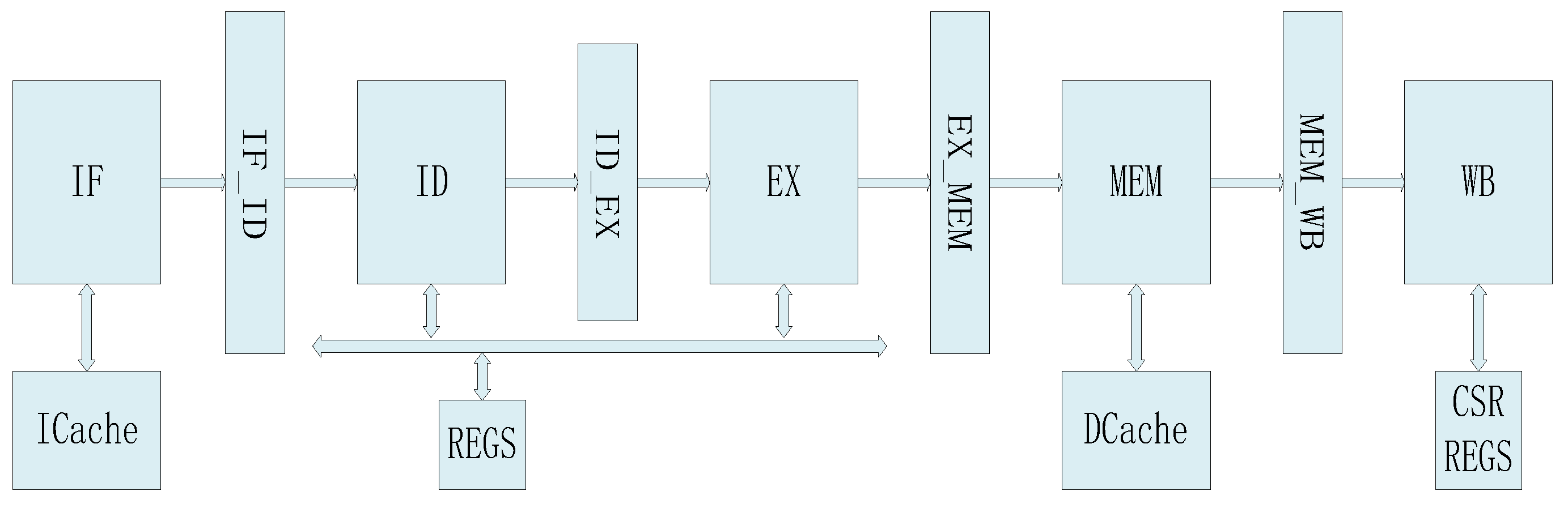
Electronics 11 00122 g001
Figure 2. Simple model of the processor core (5-stage).
Electronics 11 00122 g002
Figure 3. Simple model of the processor core (3-stage).
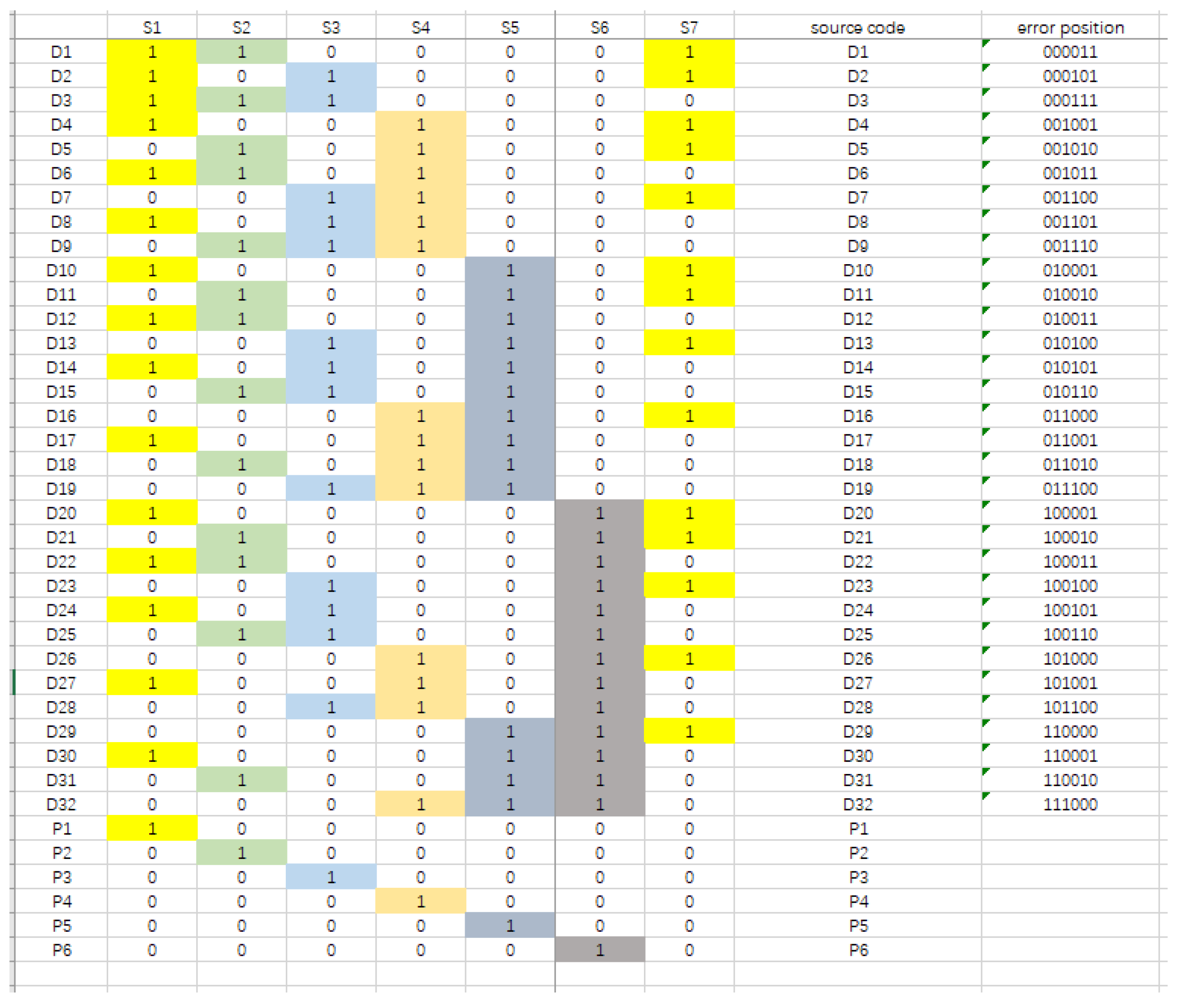
Electronics 11 00122 g003
Figure 4. Improved SECDED code encoding and verification scheme.
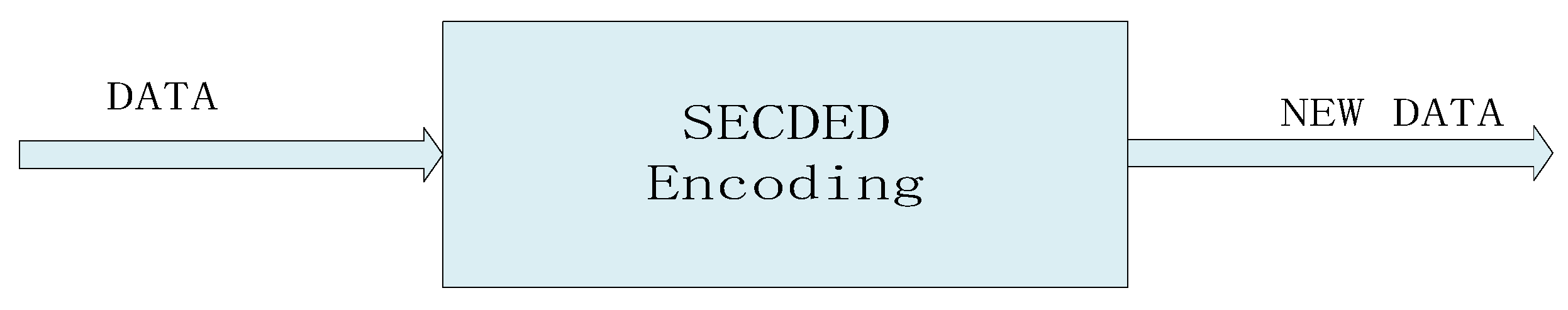
Electronics 11 00122 g004
Figure 5. Data encoding module.
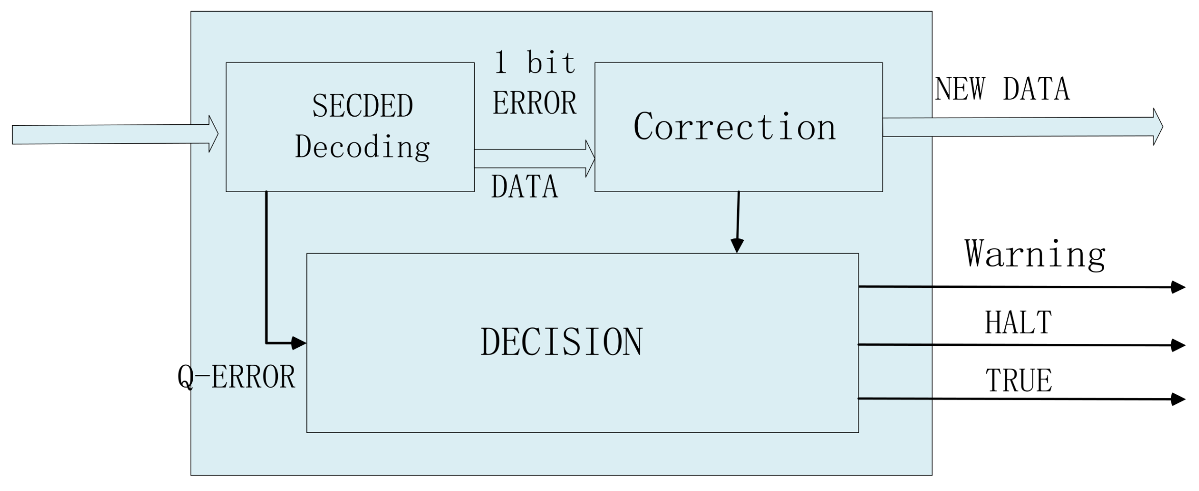
Electronics 11 00122 g005
Figure 6. Embedded data decoding module. It is embedded in a combinational logic module to realize the SECDED decoding function and correct errors in time. It will generate an alarm signal in case of a multi-bit error.
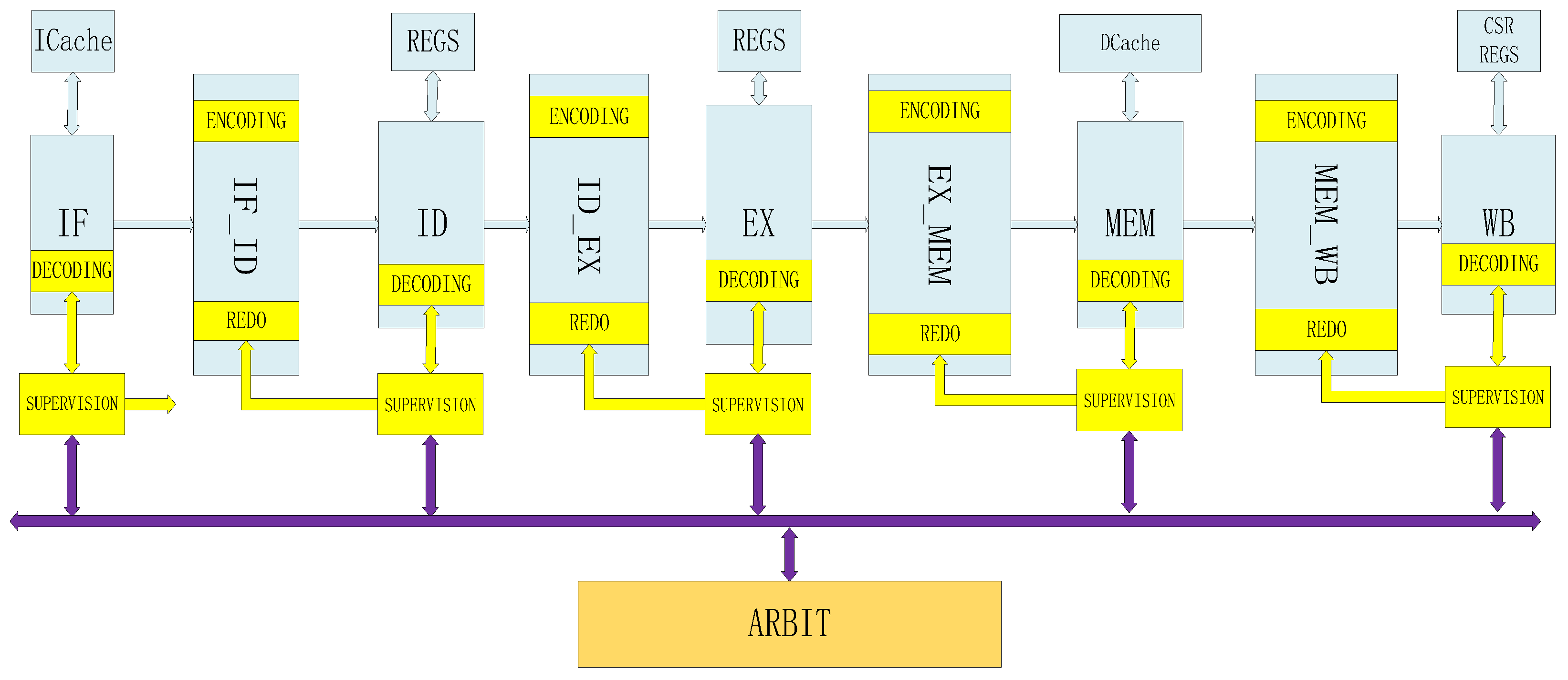
Electronics 11 00122 g006
Figure 7. Processor fault-tolerant architecture based on pipeline rollback.
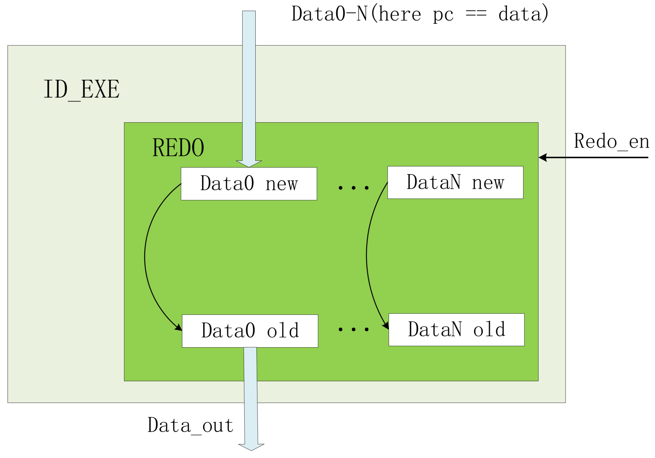
Electronics 11 00122 g007
Figure 8. REDO module: It is embedded in the timing logic module to store temporary data in real-time. When the REDO operation is performed, it realizes the function of data replacement.
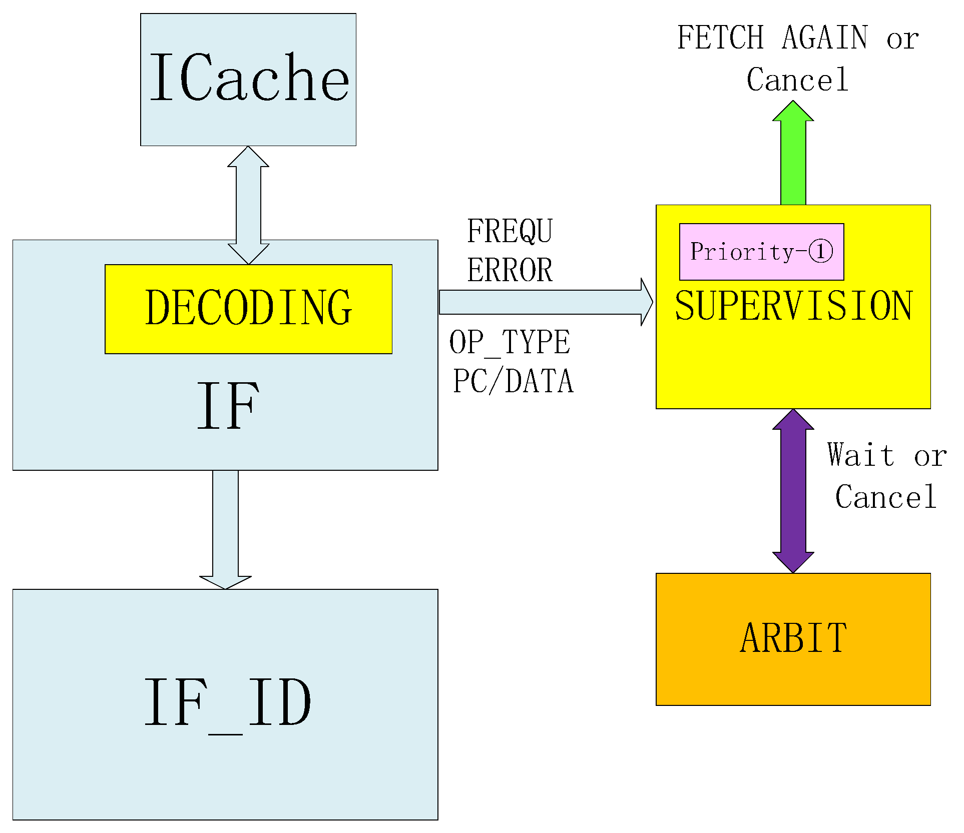
Electronics 11 00122 g008
Figure 9. Fetching rollback process. The fetching refers to fetching data from the ICache. After decoding, if there is no exception, the data will enter the next timing logic. After the exception occurs, the relevant data will be sent to the SUPERVISION module. The SUPERVISION module performs re-fetching or cancels fetching according to the processing given by the ARBIT module.
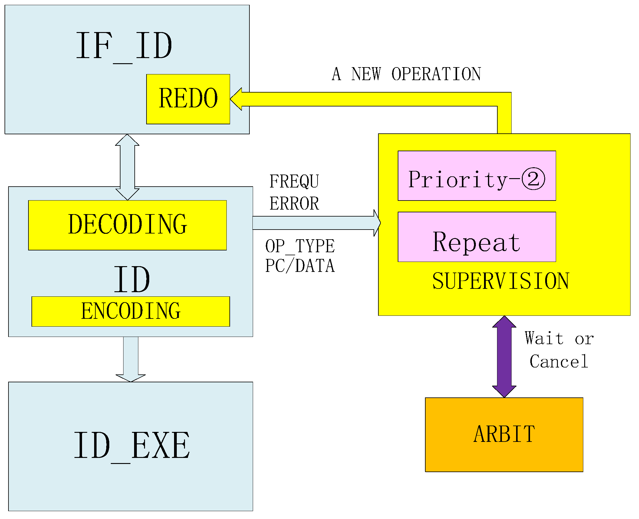
Electronics 11 00122 g009
Figure 10. Fetching-decoding rollback process. After the data from the fetching module enters the timing logic, the data without error is sent to the decoding module. If there is an exception, the REDO operation will be executed at this stage to return the original data. The REDO operation is arbitrated by the ARBIT module, and then the SUPERVISION module is notified to give feedback.
Electronics 11 00122 g010
Figure 11. Decoding Rollback Process. The execution of this module is similar to that of the fetching module, but the data does not come from the ICache. This stage also detects whether there is a decoding error and reports the data to the SUPERVISION module.
Electronics 11 00122 g011
Figure 12. Execution rollback process. The operation in this stage is similar to that in Figure 9, but the instruction type needs to be determined in this stage. Therefore, the Jump module is embedded in this module to determine whether the current execution type is a Control Transfer Instruction and report the information to the ARBIT module.
Electronics 11 00122 g012
Figure 13. Rv32IM instruction classification.
Electronics 11 00122 g013
Figure 14. Flush module: The module is embedded in the ARBIT module to determine whether the current instruction needs to be refreshed according to the received error type, priority, and instruction type. If there is an error appearing in the levels of the first–third stage, the jump situation needs to be determined.
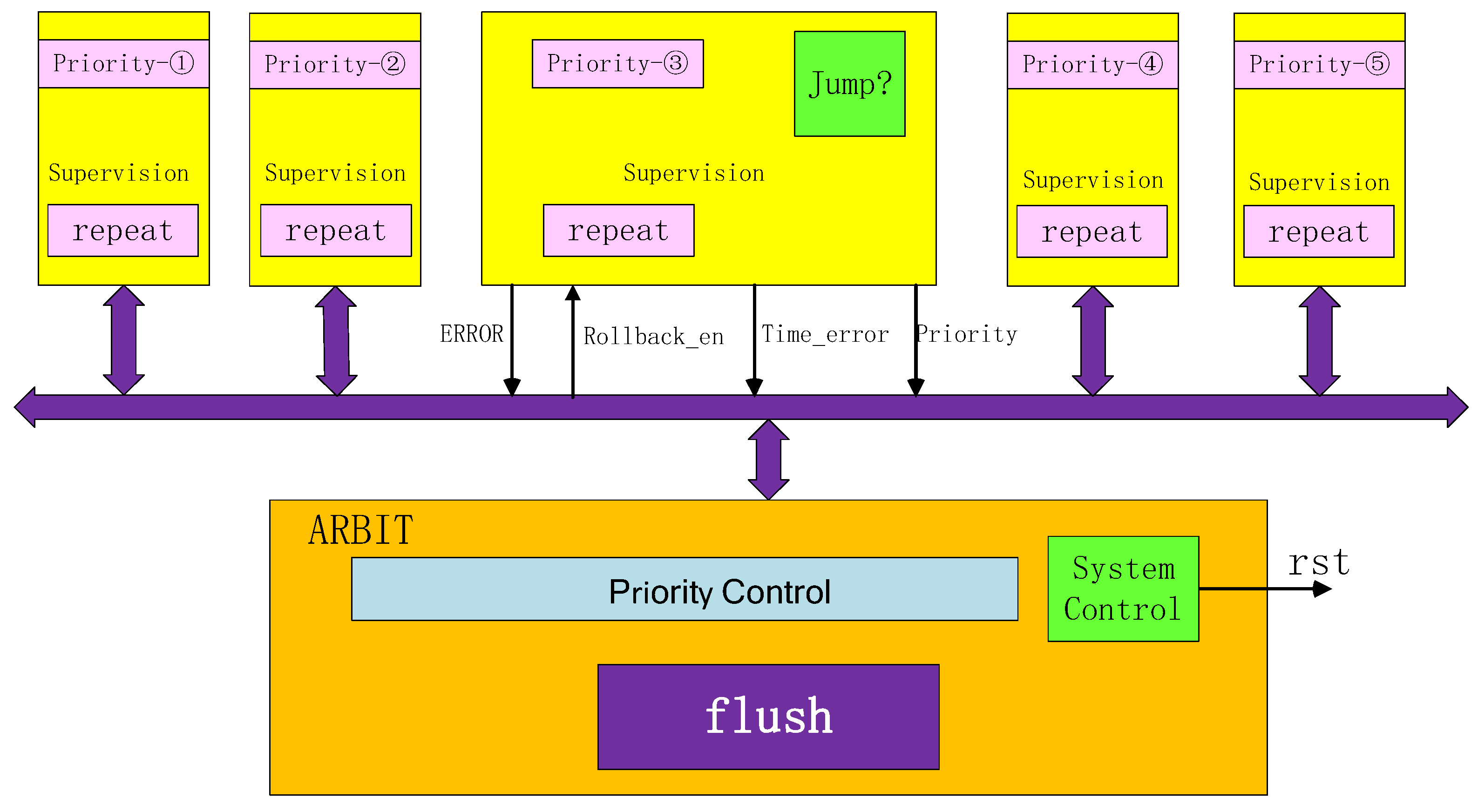
Electronics 11 00122 g014
Figure 15. The relationship between the arbiter and the supervisory module. The yellow part of the figure shows the SUPERVISION modules distributed between the 1–5 stages of the pipeline, which are distributed from left to right to monitor the error conditions of the 1–5 stages of the pipeline in turn. The SUPERVISION module summarizes the collected error signal, priority, and instruction type to the ARBIT module. The ARBIT module determines the rollback strategy through internal judgment and sends the rollback command back to each SUPERVISION module.
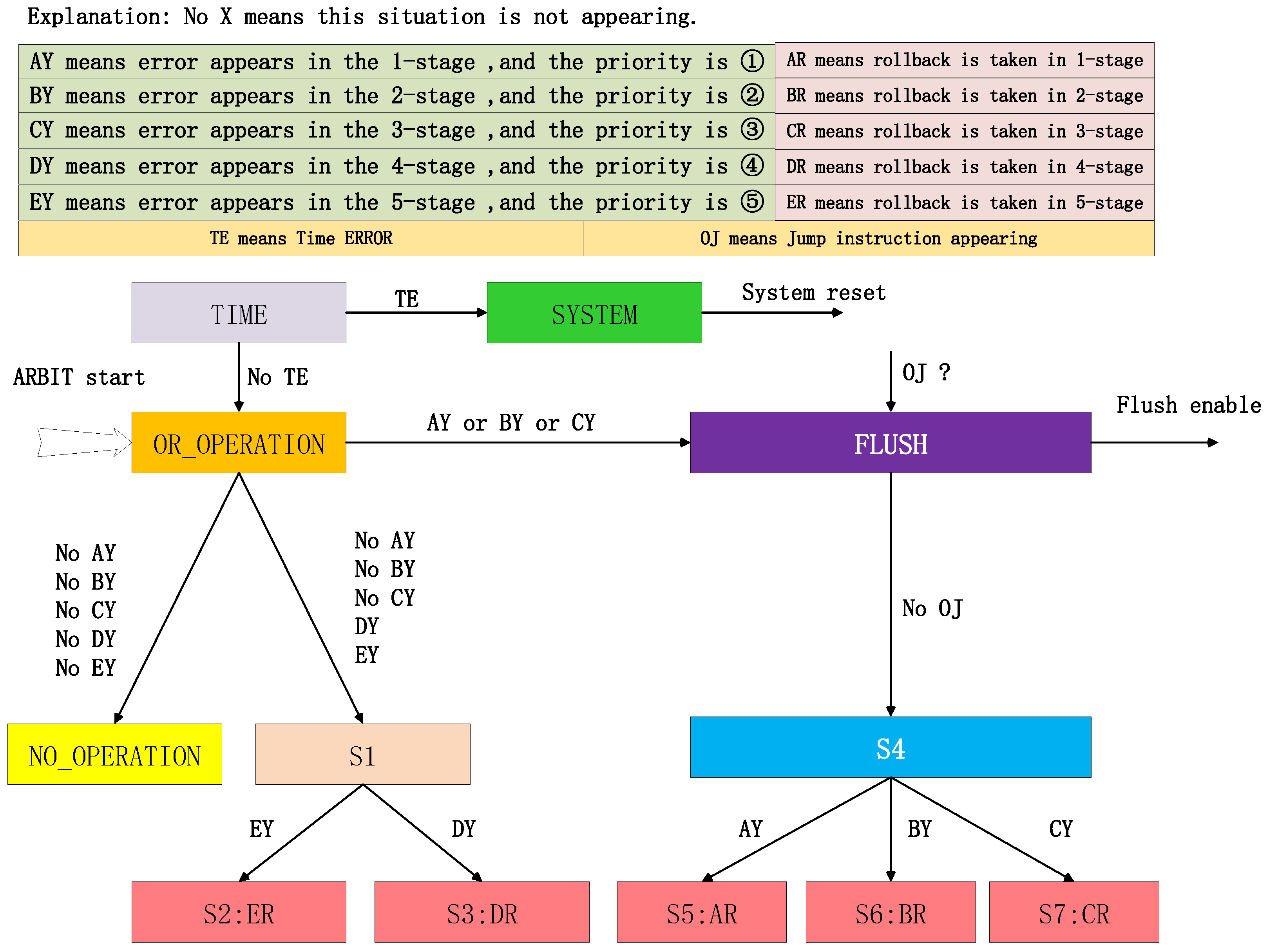
Electronics 11 00122 g015
Figure 16. Internal operation diagram of the ARBIT module.
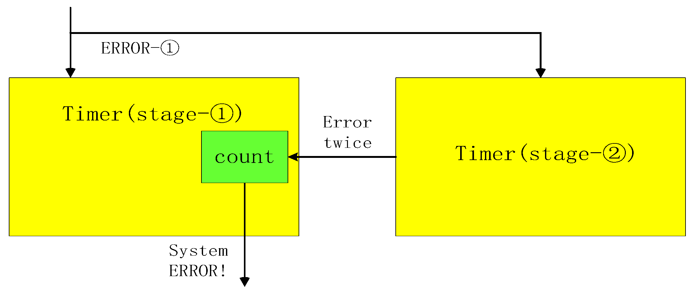
Electronics 11 00122 g016
Figure 17. Fatal error abnormal monitoring. The module is embedded between 1 to 5 stages of the pipeline and is placed at every two stages of the pipeline to monitor whether the errors between two adjacent decoding modules occur repeatedly. If the interval period is one cycle, the count will increase by 1, and a fatal information alarm will be sent after the count reaches the threshold. Then, the system generates a system ERROR.
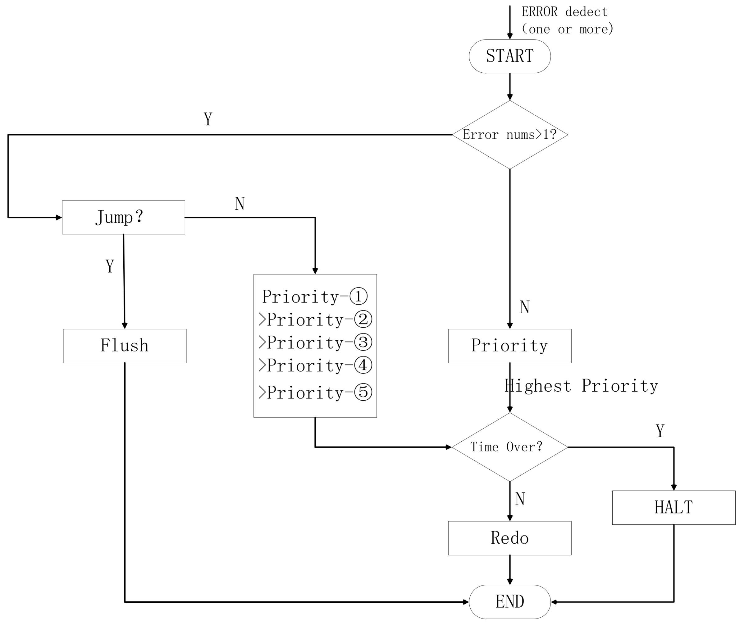
Electronics 11 00122 g017
Figure 18. Flowchart of fault-tolerant rollback operation.
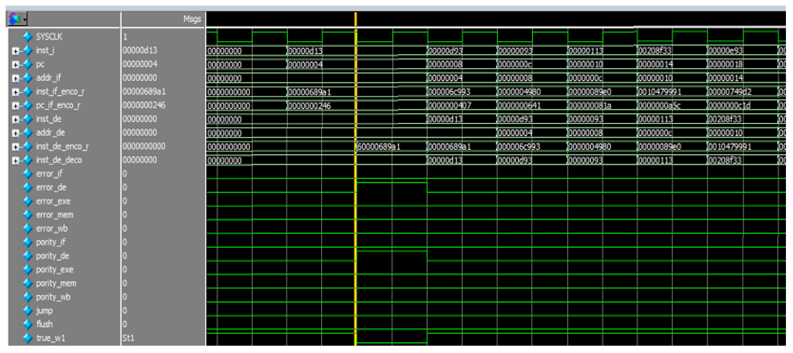
Electronics 11 00122 g018
Figure 19. Program operation abnormal data flow 1.
Electronics 11 00122 g019
Figure 20. Program operation abnormal data flow 2.
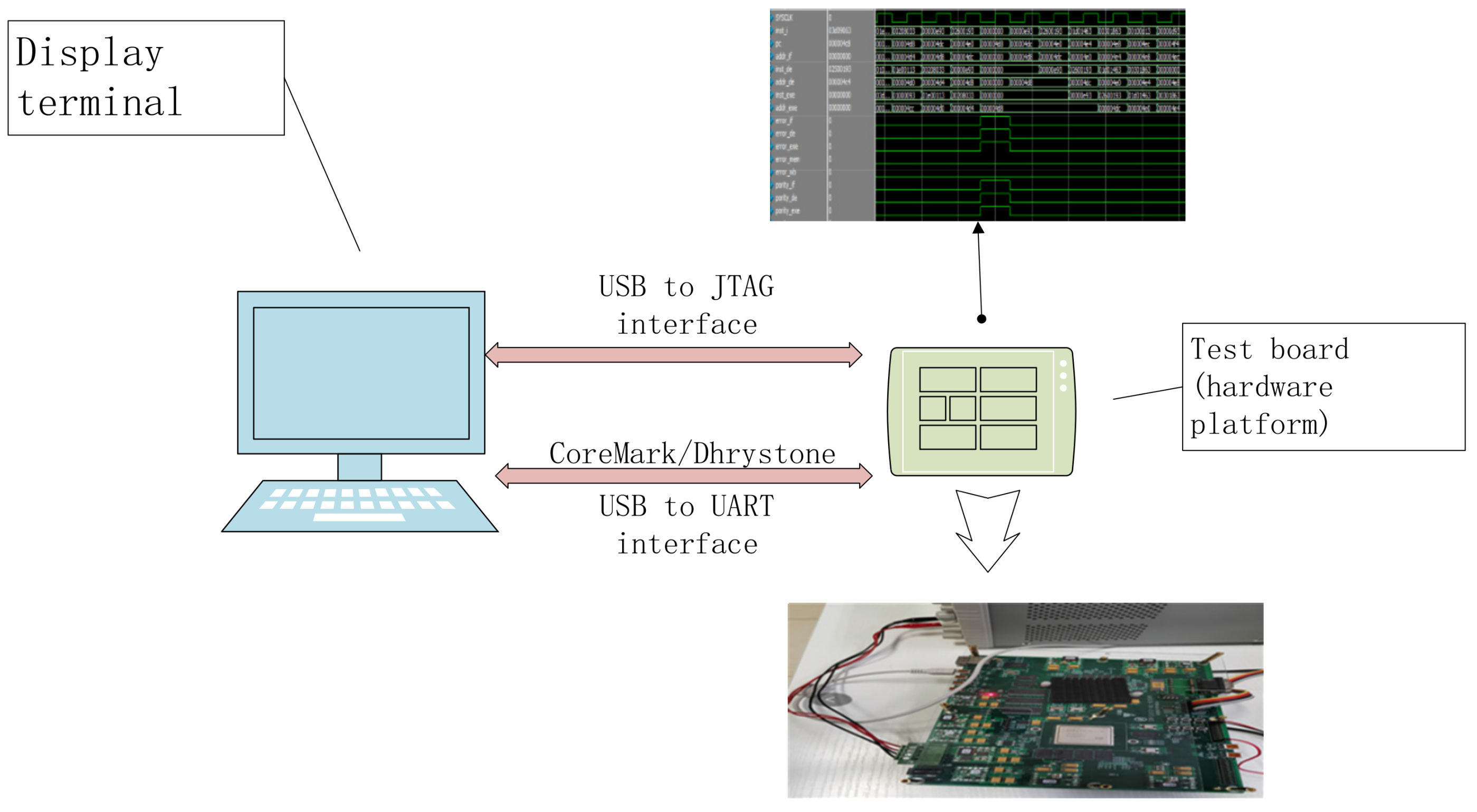
Electronics 11 00122 g020
Figure 21. Hardware interaction platform.
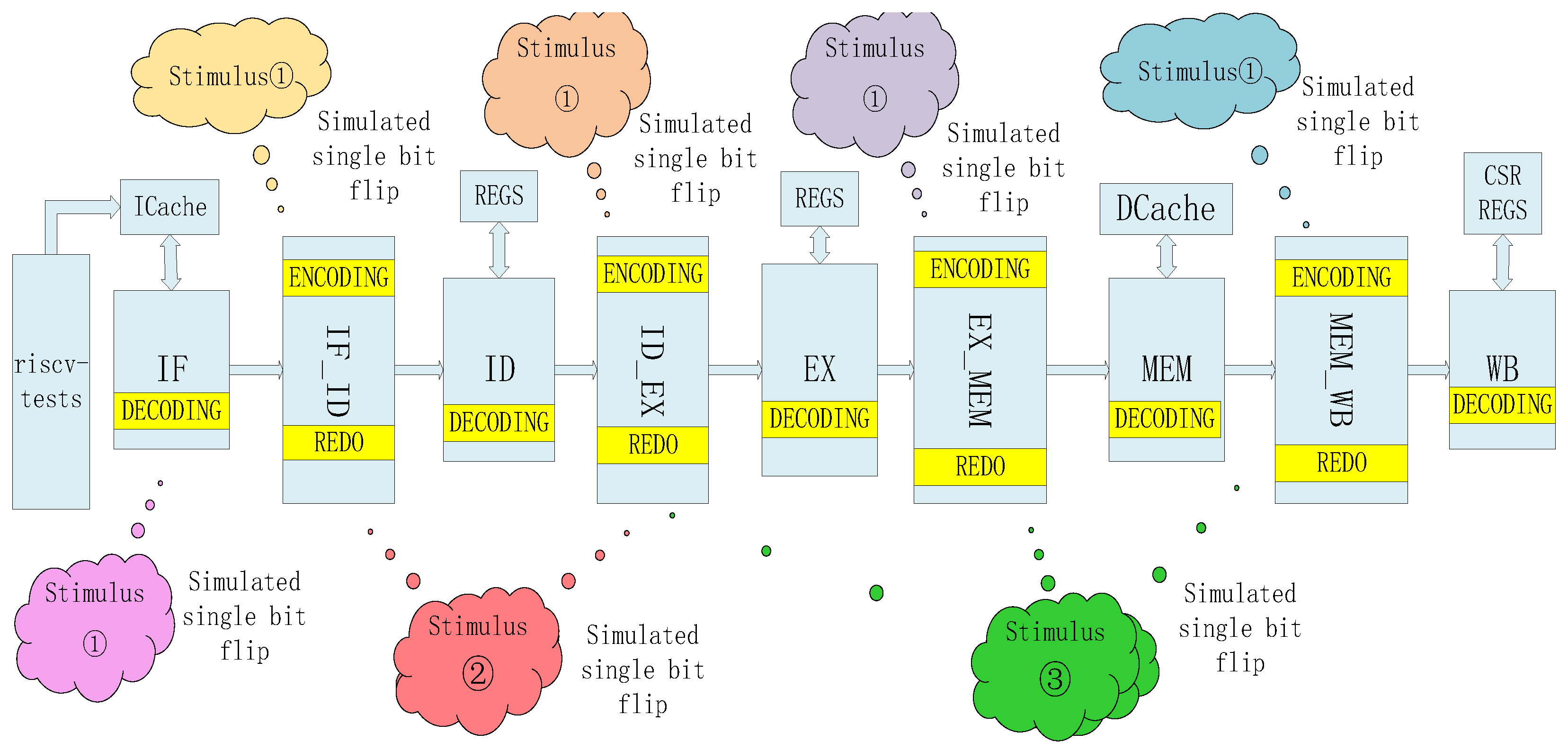
Electronics 11 00122 g021
Figure 22. Simulation test excitation diagram.
Electronics 11 00122 g022
Figure 23. Encoding embedded in the CSR control module.
Electronics 11 00122 g023
Figure 24. CSR instruction test incentive flow chart.
Electronics 11 00122 g024
Figure 25. Decoding-stage error rollback strategy.
Electronics 11 00122 g025
Figure 26. Decoding-stage error is flushed by jump instruction.
Electronics 11 00122 g026
Figure 27. Exception handling in the case of multiple errors in a single cycle.
Electronics 11 00122 g027
Figure 28. Fatal error handling diagram.
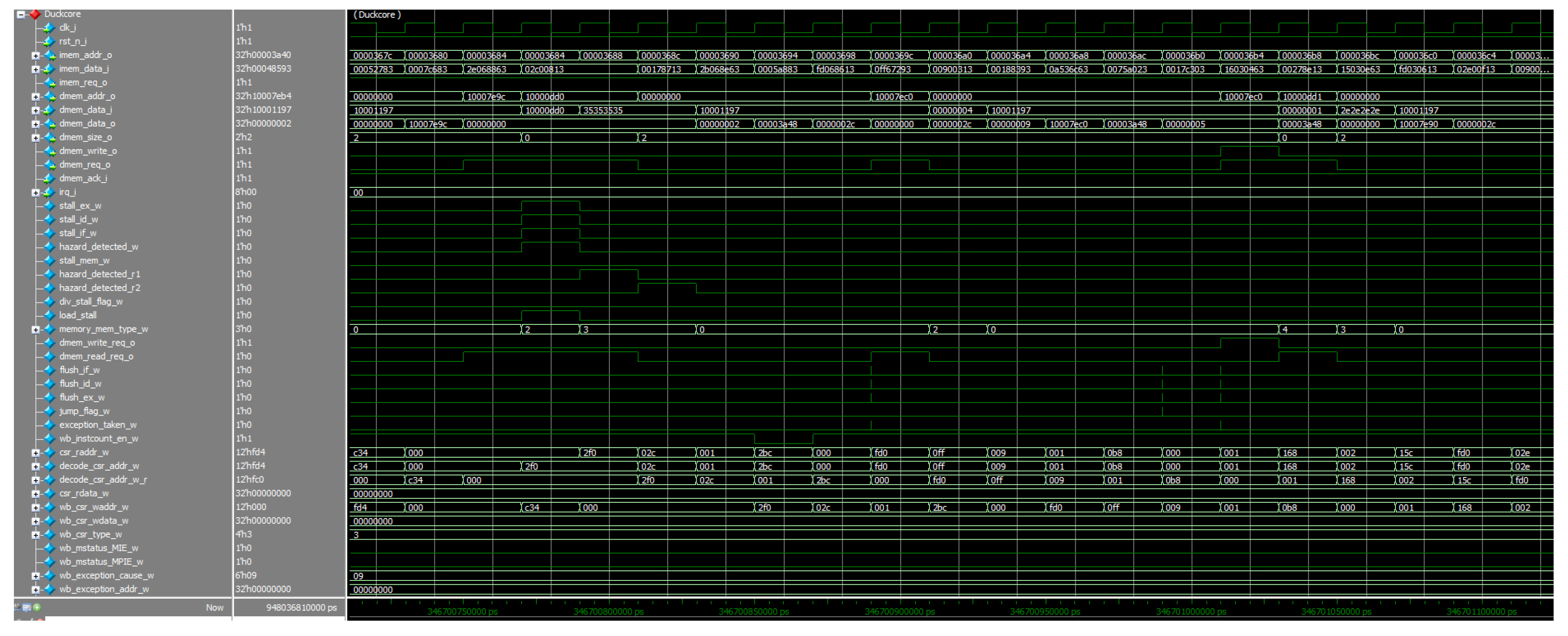
Electronics 11 00122 g028
Figure 29. CoreMark operation waveform.
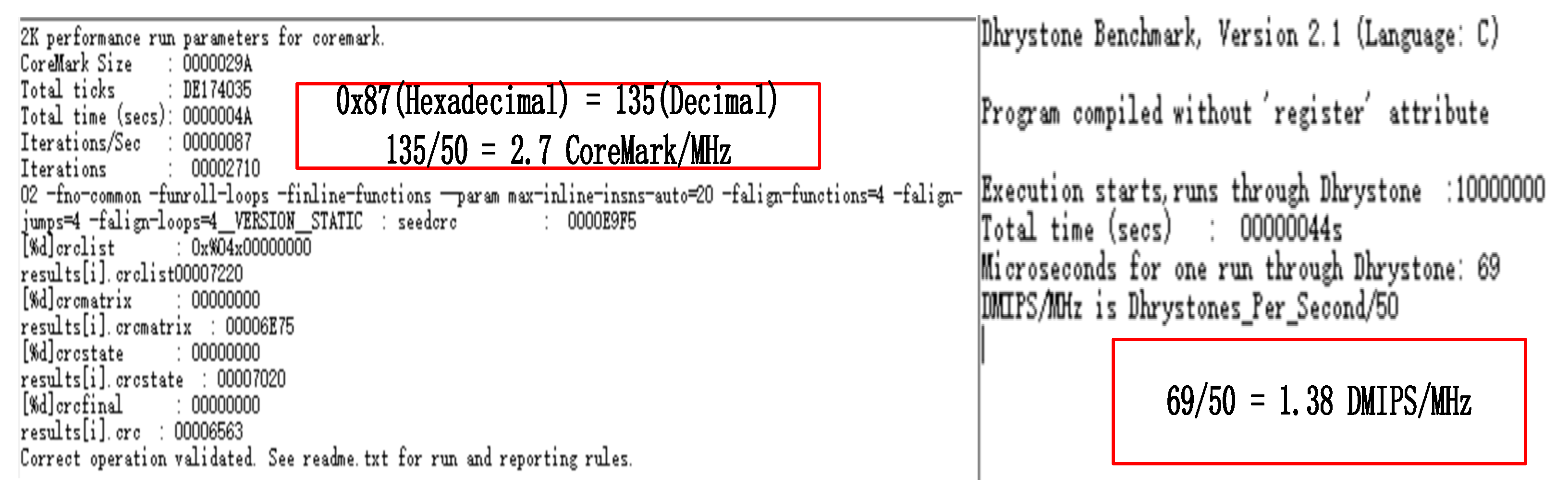
Electronics 11 00122 g029
Figure 30. Operation result display diagram of CoreMark and Dhrystone.
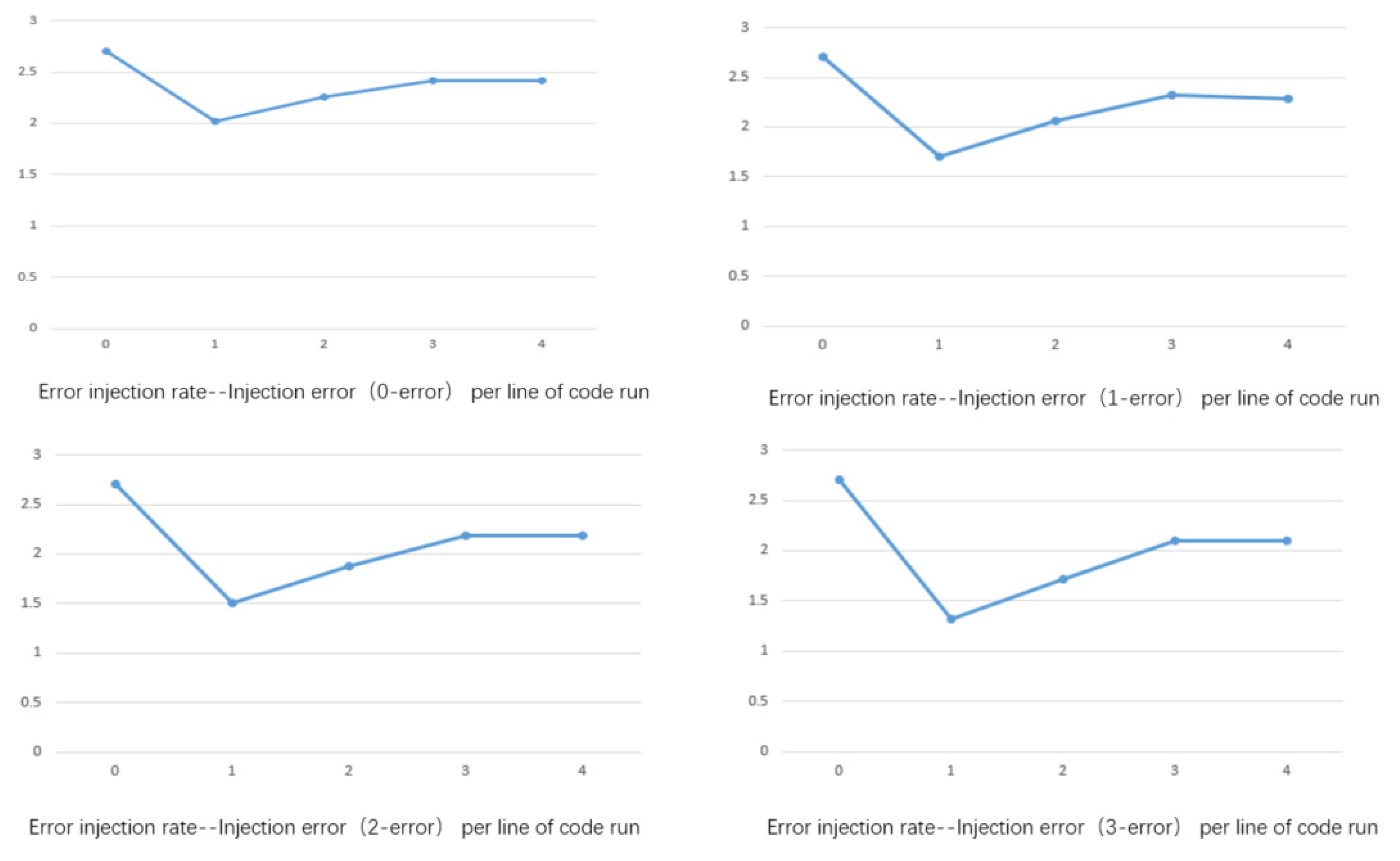
Electronics 11 00122 g030
Figure 31. Dhrystone running scores under different error injection frequencies.
Electronics 11 00122 g031
Figure 32. CoreMark running scores under different error injection frequencies.
Electronics 11 00122 g032
Table 1. Running results of CoreMark and Dhrystone under different error injections.
X-ErrorsAbscissaCoreMarkDhrystone
012.020.92
022.261.1
032.401.18
042.421.2
111.70.68
122.060.96
132.271.08
142.281.14
211.50.6
221.880.78
232.161
242.181.06
311.320.68
321.720.72
332.10.92
342.121.01
Table 2. Comparison of resources occupied by fault-tolerant solutions of different open-source cores.
Processor CoreISASlice LUTsSliceLUT as Logic
DuckCoreRv32IM2916(1.43%)2662916
DuckCore (change Architecture)Rv32IM3073(1.5%)20933073
V-scaleRv32IM2700(1.32%)10032700
V-scale (change Architecture)Rv32IM2700(1.32%)19042700
UltrascaleRv32IM3598(1.77%)27063598
Ultrascale (change Architecture)Rv32IM4223(2.07%)42233598
TinyriscvRv32IM5754(2.82%)19845754
Tinyriscv (change Architecture)Rv32IM5754(2.82%)26375754
Table 3. Comparison of resource occupation under different codes.
Processor CoreSlice LUTs
Ultrascale3598(1.77%)
Ultrascale (use Classic SECDED)4877(1.77%)
Ultrascale (use improved SECDED)4223(2.07%)
DuckCore2916(1.43%)
DuckCore (use Classic SECDED)3621(1.78%)
DuckCore (use improved SECDED)3073(1.5%)
Table 4. Comparison of power consumption under different codes.
Processor CoreTotal on-Chip Power
DuckCore0.214 W
DuckCore (change Architecture with Classic SECDED)0.244 W
DuckCore (change Architecture with improved SECDED)0.227 W
Table 5. Comparison of different processor core indicators.
Processor CoreISACoreOne-Bit ErrorTwo-Bit ErrorM-Bit Error
DuckCoreRV32IM1YY—support 1–5piplePart support
SHAKTI-FRv32I1YY—support 3pipleNo support
DIVASPARC2Part supportPart supportPart support
Publisher’s Note: MDPI stays neutral with regard to jurisdictional claims in published maps and institutional affiliations.

