

Low-Temperature and Room-Temperature Surface-Activated Au–Au Bonding: Surface Requirements, Preparation Methods, and Emerging Applications

 , , , and
Abstract
1. Introduction
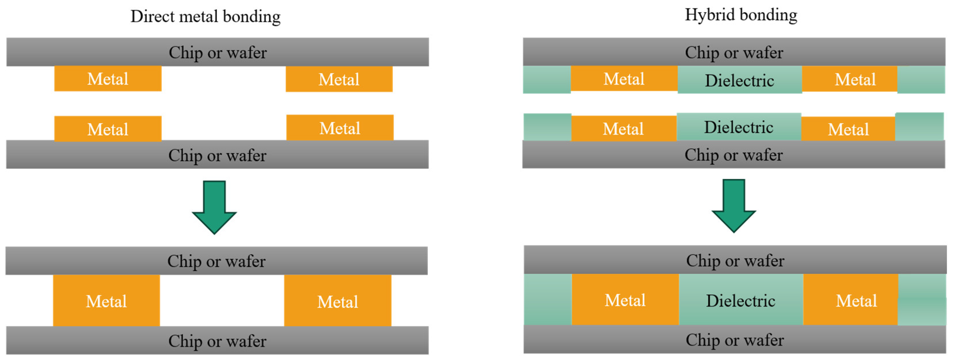
1.1. Direct and Hybrid Bonding
1.2. Review Scope
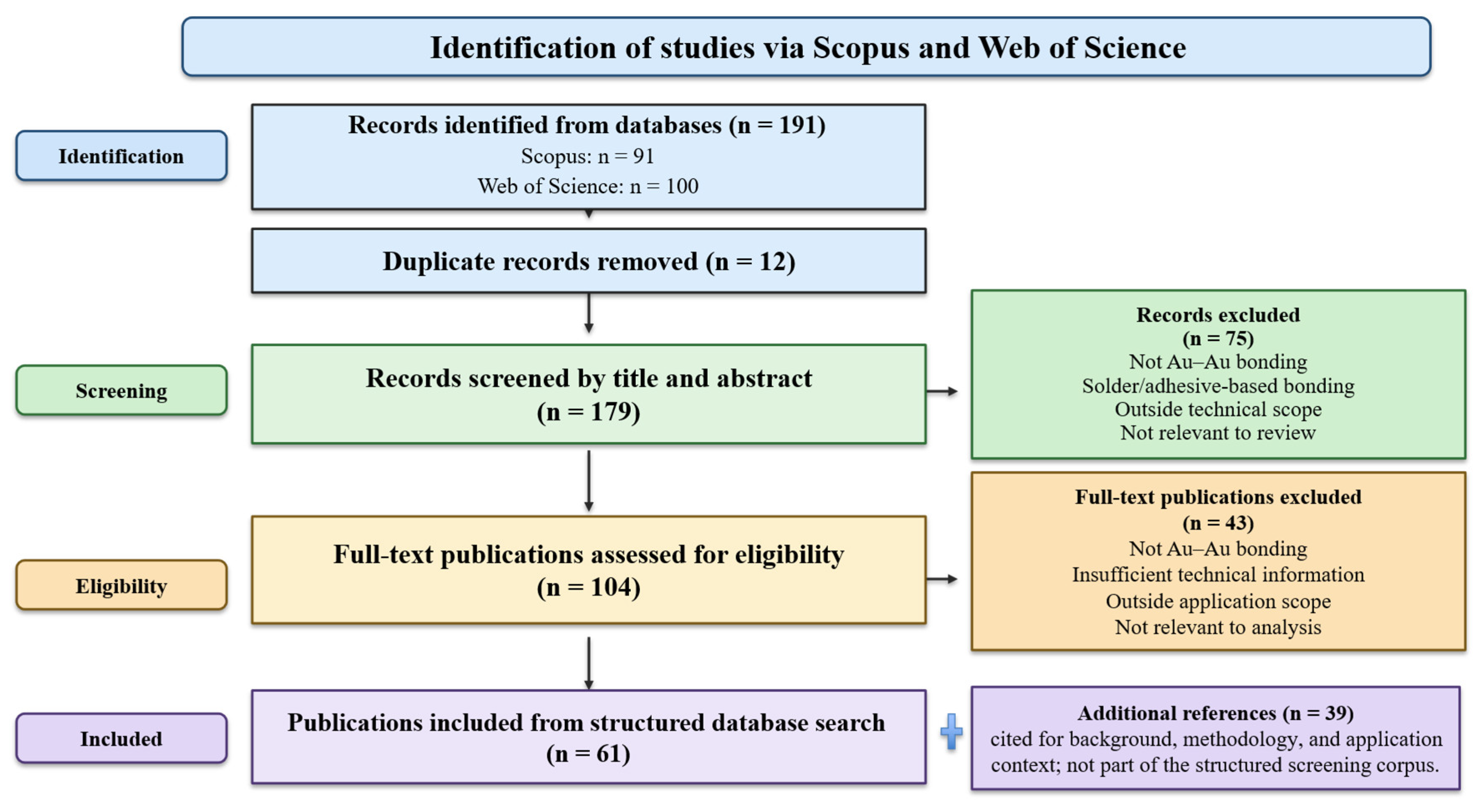
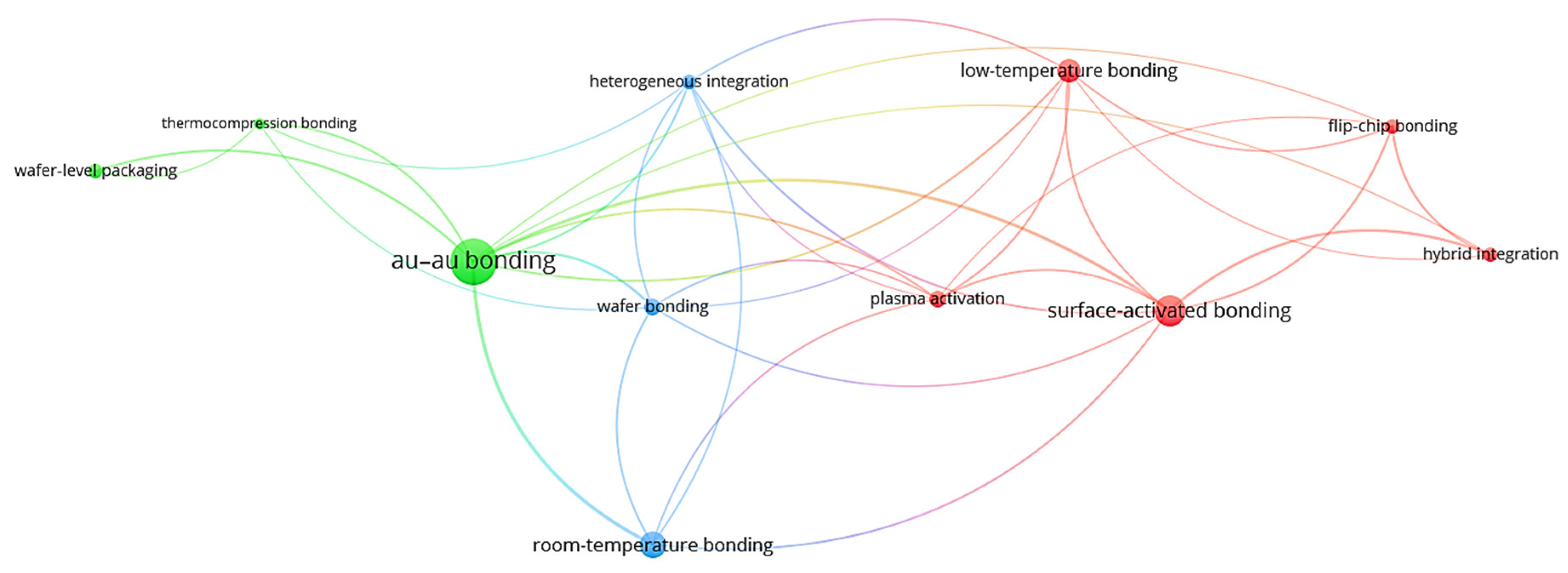
1.3. Review Methodology
2. Position of Au–Au Bonding in Advanced Integration
3. Bonding Routes for Solid-State Au–Au Joining
3.1. TCB Baseline
3.2. Low-Temperature Surface-Engineered Direct Bonding
3.2.1. Surface Roughness Control in Direct Bonding
3.2.2. Surface Activation Methods for Low-Temperature Au–Au Bonding
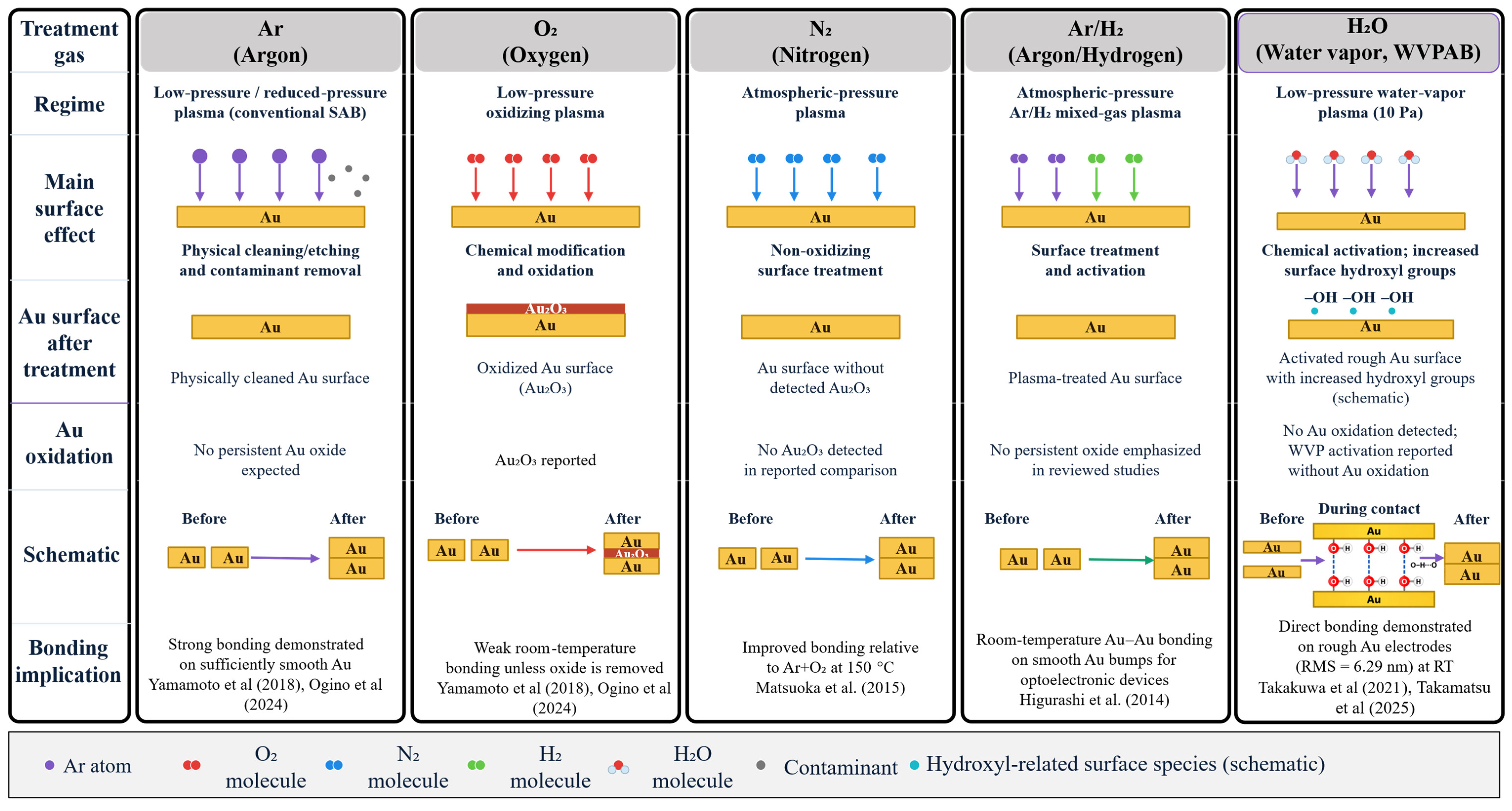
- Low-Pressure Plasma and Beam Activation
- B.
- Ar Plasma and Fast-Atom-Beam Activation
- C.
- Oxygen-Containing Plasma and Oxidation
- D.
- Atmospheric-Pressure Plasma Activation
- E.
- Ar and Ar/H2 Atmospheric-Pressure Plasma
- F.
- N2 Atmospheric-Pressure Plasma
- G.
- VUV, UV/O3, and Sequential Photochemical–Plasma Activation
- H.
- WVPAB for Rough and Flexible Substrates
3.2.3. Contamination Control and SAM-Based Surface Protection
3.2.4. Intermediate-Assisted Low-Temperature Au-Based Bonding
3.3. Mechanisms of Au–Au Bonding
4. Device-Level Applications of Au–Au Low-Temperature Bonding
4.1. Optical and Optoelectronic Devices
4.2. MEMS Hermetic and Vacuum Packaging
4.3. Heterogeneous Integration and RF/Acoustic Devices
4.4. Flexible Hybrid Electronics
5. Metrology for Au–Au Bonding
6. Reliability Limits and Performance Constraints
6.1. Yield Limiters
6.2. Mechanical Integrity
6.3. Electrical Functionality and Stability
6.4. Stress-Specific Reliability and Benchmarking
7. Research Gaps and Future Directions
8. Conclusions
Author Contributions
Funding
Institutional Review Board Statement
Informed Consent Statement
Data Availability Statement
Conflicts of Interest
Abbreviations
| Abbreviation | Full form |
| AFM | Atomic force microscopy |
| Ar | Argon |
| Au | Gold |
| CMOS | Complementary metal–oxide–semiconductor |
| CMP | Chemical mechanical polishing |
| CMUT | Capacitive micromachined ultrasonic transducer |
| CTE | Coefficient of thermal expansion |
| DDT | Dodecanethiol |
| EDX | Energy-dispersive X-ray spectroscopy |
| FAB | Fast atom beam |
| FBAR | Film bulk acoustic resonator |
| FHE | Flexible hybrid electronics |
| FIB | Focused ion beam |
| H2 | Hydrogen |
| HI | Heterogeneous integration |
| IC | Integrated circuit |
| I/O | Input/output |
| L-I-V | Light-current-voltage |
| L/S | Line/space |
| LSI | Large-scale integrated circuit |
| LTCC | Low-temperature co-fired ceramic |
| MEMS | Microelectromechanical systems |
| MIL-STD | Military standard |
| N2 | Nitrogen |
| NP | Nanoparticle |
| O2 | Oxygen |
| OLED | Organic light-emitting diode |
| PI | Polyimide |
| PRISMA | Preferred Reporting Items for Systematic Reviews and Meta-Analyses |
| RF | Radio frequency |
| RF-MEMS | Radio-frequency microelectromechanical systems |
| RGP | Residual gas pressure |
| RMS | Root mean square |
| RT | Room temperature |
| SAB | Surface-activated bonding |
| SAM | Self-assembled monolayer |
| SAW | Surface acoustic wave |
| TCB | Thermocompression bonding |
| TEM | Transmission electron microscopy |
| TSV | Through-silicon via |
| UHV | Ultra-high vacuum |
| UV/O3 | Ultraviolet/ozone |
| VCSEL | Vertical-cavity surface-emitting laser |
| VUV | Vacuum ultraviolet |
| WVPAB | Water-vapor plasma-assisted bonding |
| XPS | X-ray photoelectron spectroscopy |
Appendix A

| Study | Bonding Route | Bonding Temperature (°C) | Pressure/Load | Bonding Time | Au Thickness/Interface Stack | Activation/Pretreatment | Geometry | Surface Roughness | Bond Strength | Electrical/Hermetic/Reliability Outcome |
|---|---|---|---|---|---|---|---|---|---|---|
| [34] | TCB | =250 | 100–350 MPa | 10–20 s | NR | NR | Au pillars = 5 × 5 × 5 µm3; InP die = 100 µm | Pillar RMS = 40 nm | 38–238 MPa | ≤1.5 Ω/die; 500 thermal cycles; 100% survived |
| [18] | TCB | 350 | 220–250 N | 250–500 s | Au pillars: 50 µm diameter, 200 µm pitch, 2–3 µm height | No specific surface-activation treatment reported; passivation-free TCB | 21 × 20 array = 420 bonds | NR | Average shear strength = 128 MPa | All 21 daisy chains electrically connected |
| [38] | TCB + Si–Si | 380 | 7000 mbar | 1 h | Ti/Au = 40/200 nm | O2-plasma treatment used for Si–Si hydrophilic prebonding, not as Au-surface activation before Au–Au TCB | Package = 9.1 × 8.5 mm2; cavity = 9.0 ± 0.2 µm | NR | Average packaging strength = 26 MPa | Static capacitance yield > 77%; hermeticity yield > 90% |
| [58] | SAB | 150 | 500 gf | 30 s contact | VCSEL electrode: Ni 3 µm/Au 100 nm; substrate Au = 500 nm | Ar RF plasma, 100 W, 30 s | Electrode diameter = 50 µm | NR | Bond strength = 84 MPa | Normal VCSEL operation after bonding |
| [59] | SAB | 25–200 | 50–900 gf | 30 s | VCSEL electrode: Ni 3 µm/Au 100 nm; substrate Au = 500 nm | Ar RF plasma: 100 W, 0–180 s | NR | RMS = 5.6 nm before plasma and 7.0 nm after 30 s Ar plasma | Representative condition (150 °C, 500 gf, 30 s plasma): strength > 50 gf, corresponding to about 54 MPa | No L-I-V degradation |
| [63] | SAB | RT | Manual contact | - | Au < 50 nm | Ar RF plasma = 100 W, 30 s; contact within 5 min | NR | RMS < 0.5 nm; 15 nm Au: 0.24 nm; 75 nm Au: 1.14 nm | 47–70 MPa | Atomic-scale TEM interface |
| [64] | SAB | RT | No compressive load | Manual contact | Au = 30 nm; Ti = 3 nm | Air exposure = 33–2000 h; Ar RF plasma = 30 s | NR | Rrms = 0.43 nm; plasma: 0.39–0.42 nm | 48–72 MPa | Bonding front < 1 s; atomic-scale TEM after 2000 h |
| [67] | Plasma-SAB | RT | Manual contact | - | Au = 15 nm; Ti = 5 nm | Plasma = 30–120 s; anneal test = 150 °C, 10 min | NR | RMS = 0.38 nm; O2 contact angle < 5° | Ar: >2.5 J/m2/wafer fracture; O2: 0.1–0.2 J/m2; O2 + anneal: 2.5 J/m2 | Au2O3 desorption = 110 °C |
| [41] | Imprint + SAB | Final bonding: room temperature; imprint = 200 °C | Imprint = 150 MPa; final bonding load = 40 kN | - | Electroplated Au around 10 µm thick; opposing Au film = 50 nm | Ar fast-atom-beam treatment | - | Sq 16 to 3 nm; Sz 113 to 53 nm | >200 MPa | NR |
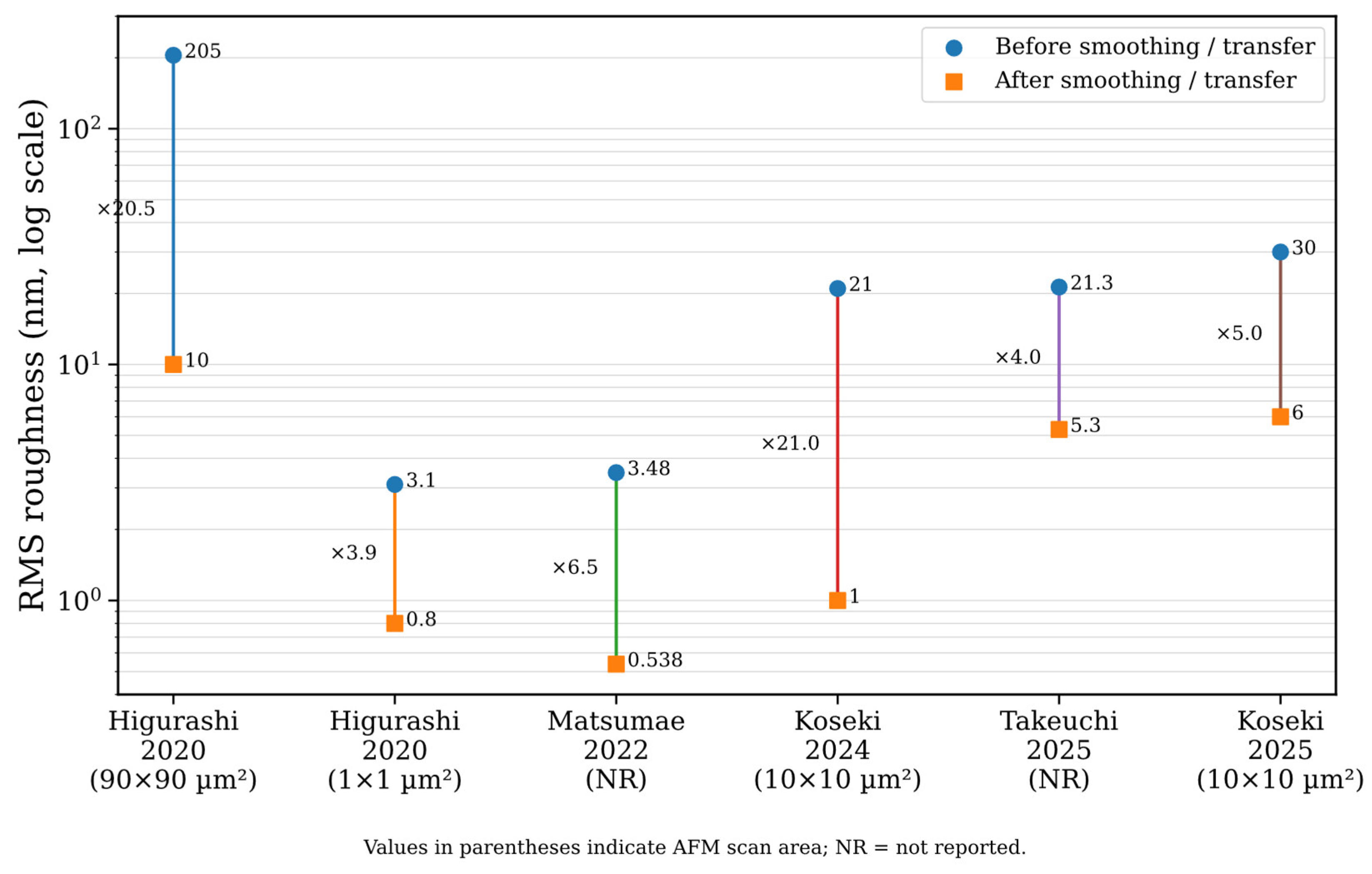
| [48] | Transfer + SAB | 150 | Transfer = 200 MPa; final bonding = 75 MPa | 600 s | Target rough Au = 200 nm on 20 nm Ti; transferred Au film = 300 nm; opposing smooth Au film = 200 nm | Ar/H2 atmospheric-pressure plasma; smoothing transfer: 150 °C, 200 MPa, 60 s | - | RMS: 205 to 10 nm over 90 × 90 µm2; RMS: 3.1 to 0.8 nm over 1 × 1 µm2 | around 15 MPa (read from figure); bulk/substrate fracture | NR |
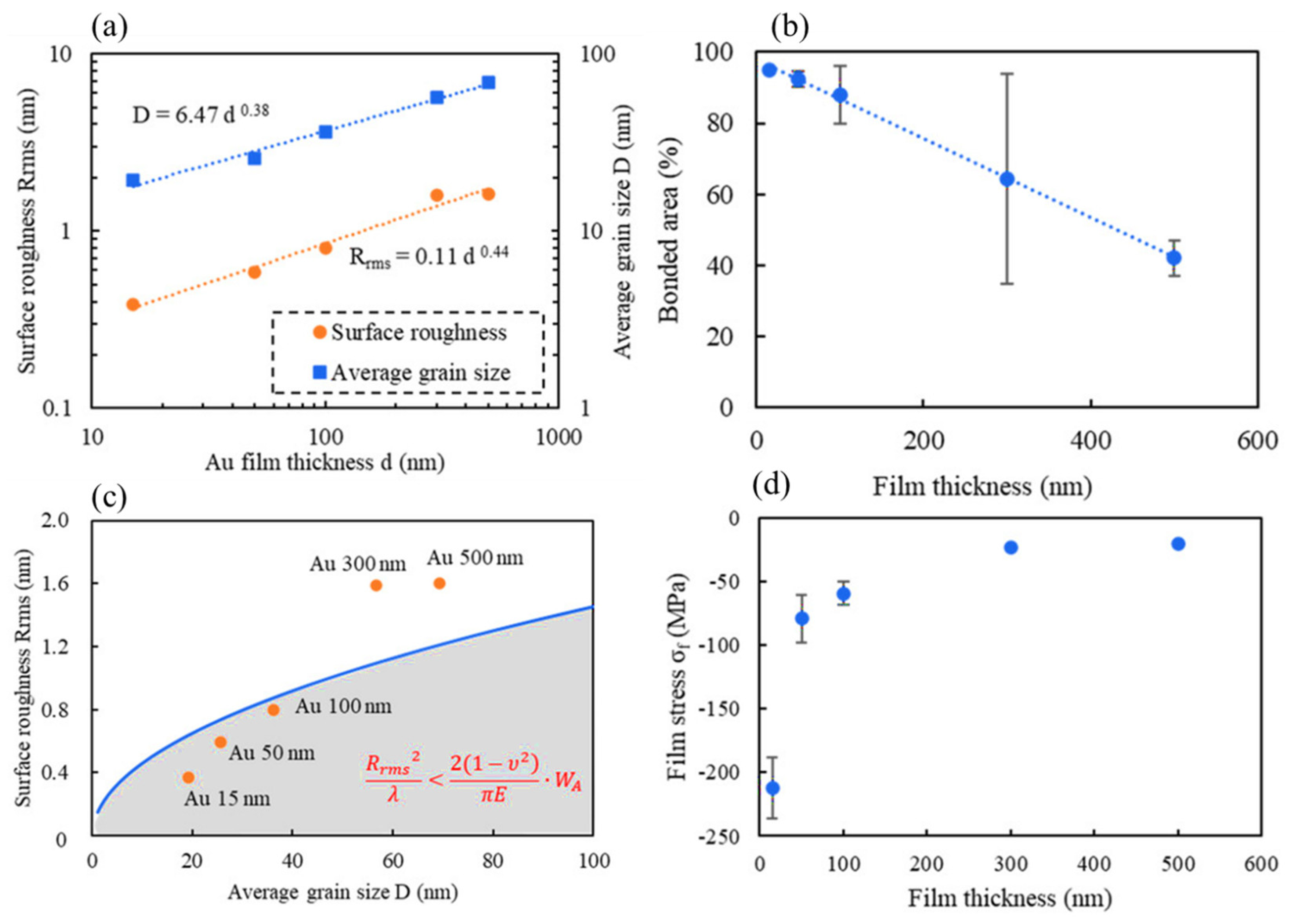
| [49] | SAB sealing | Room temperature | <1.6 MPa | - | Au = 15–500 nm; Ti = 5 nm | Ar-plasma activation = 60 s | AFM scan = 500 × 500 nm2 | RMS = 0.3–1.6 nm | Bonded area > 85% for Au ≤ 100 nm | Vacuum sealing achieved for Au ≤ 50 nm |
| [99] | TCB sealing | 300 | 40 MPa | 30 min | Au signal line = 1 µm; SiOx = 2–12 µm | Activation: Ar plasma immediately before bonding; vacuum around 5 × 10⁻³ Pa | Planarized Au seal-ring surface | around 1 nm (Ra) | NR | Cavity pressure around 500 Pa or lower; vacuum maintained for >19 months; leak rate < 8 × 10⁻¹⁶ Pa·m3/s |
| [7] | WVPAB | RT | =2 N for 5 s; no sustained load | ≥12 h after overlap | 2 µm parylene; Cr/Au = 3.5/50–100 nm | Water-vapor plasma = 50 W, 40 s | NR | RMS = 6.29 nm; smooth Au RMS = 1.8 nm | Substrate failure in peel test | Contact area < 50 × 50 µm2; L/S = 10 µm; <1% ΔR after 10,000 cycles |
| [53] | Getter-layer SAB | Room temperature | Bonding pressure = 123 kPa | - | Getter layer: Au/Ti/Au = 20/100/20 nm; opposing bonding layer: Au/Ti = 20/5 nm | Ar plasma = 200 W, 30 s; vacuum = 1 × 10⁻² Pa | NR | RMS = 3.48 to 0.538 nm | Strength > 26 MPa | Unbonded area = 9.5% |
| [19] | Au–Au thermal interface | 300 | Pressure = 7–11 MPa; optimum = 9 MPa | 30 min (Methods; abstract states 1 h) | Ti/Ni = 20/20 nm; Au thickness = 100, 300, and 500 nm | No CMP and no post-anneal (ICP substrate treatment not classified as Au surface activation) | NR | RMS = 1.18, 1.77, and 2.29 nm, respectively | Mechanical bond strength = NR | 500 nm Au gave 99% bonding ratio; thermal conductivity = 101.32 W·m−1·K−1 |
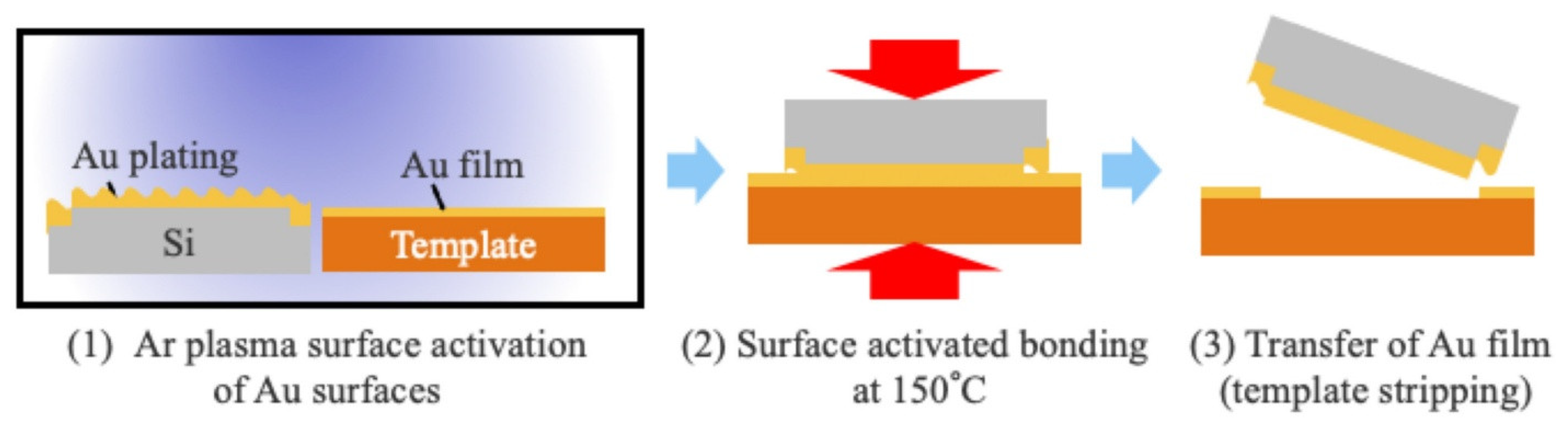
| [50] | PI/SiO2 template stripping + SAB | Smoothing = 150 °C; final bonding = 30 °C | Smoothing = 75 MPa; final bonding = 30 MPa | 600 s | Plated Au = 1.25 µm; template Au = 100 nm; opposing Au = 15 nm | Ar RF plasma | - | RMS = 21 nm to around 6 nm after PI transfers to around 1 nm after additional SiO2/Si transfer | Strength not assigned an exact MPa value (primarily read from plotted data); MIL-STD-883 criterion satisfied; Si bulk fracture | NR |
| [52] | PI template stripping + SAB | Smoothing = 150 °C; final bonding = 30 °C | Smoothing = 75 MPa; final bonding = 10 MPa | 10 min | Plated Au = 1.2 µm; template Au = 100 nm; opposing Au = 15 nm | Smoothing activation: Ar RF plasma, 200 W, 1 min; final activation: Ar plasma, 150 W, 30 s | - | RMS around 21.3 to around 5.3 nm over 10 × 10 µm2 after repeated PI template stripping | Strength > 15 MPa with bulk fracture | NR |
| [51] | Bump smoothing + SAB | Smoothing = 150 °C; final bonding = 30 °C | Smoothing = 75 MPa/bump; final bonding = 30 MPa/bump | 10 min in air | Template Au = 100 nm; opposing Au = 15 nm | Smoothing activation = Ar fast atom beam for 5 min | Au bumps = 100 µm diameters, around 2.5 µm height, 400–500 µm pitch | RMS = around 30 to around 6 nm after three PI transfers, 10 × 10 µm2 AFM area | Bond strength = NR, because the paper does not report a quantitative final strength | NR |
| [76] | WVPAB flexible device | RT; post-anneal = 200 | Hand press; force NR | - | Si sensor = 5 µm; parylene = 2 µm; piezoresistor = 150 nm | Water-vapor plasma = 50 W, 40 s; post-anneal = 1 h | - | Au pad RMS = 1.4 nm; Au wiring RMS = 0.4 nm | Peel: sensor/substrate failure | 10,000 bending cycles; no noticeable drift/degradation; sensitivity = 0.0712 per mm−1 curvature |
| [100] | TCB | 150–175 | 250–450 N | 10–20 min | NR | NR | Au pillars: 25 µm diameter, 100 µm pitch, 3–5 µm height | Ra = 5–10 nm | 444.53 MPa at 150 °C; 573.91 MPa at 175 °C; cohesive Au failure | 17 daisy chains showed electrical continuity. |
| [94] | Room-temperature direct bonding/cold welding | RT/low-T | Pressure investigated from 40 kPa to 10 MPa (10 MPa could damage the nanomesh); robust bonding around 1 MPa | Sufficient bond formation within around 3 s (pressing 10 s) | NR | No surface activation and no adhesive | Au-coated nanomesh interface | NR | T-peel strength around 10–20 N/m | Resistance change remained within 5% after 8000 bending cycles at 1 mm radius; EDX showed no C/O segregation |
References
- Huang, M.; Xia, Y.; Han, X.; Gao, Y.; Chen, S.; Cui, Z.; Zhang, C.; Gao, Y.; Qiao, Z.; Lv, Y.; et al. High-strength Au–Au bonding for temperature and pressure integrated sensor. J. Mater. Res. Technol. 2025, 35, 1239–1249. [Google Scholar] [CrossRef] [Scilit]
- Ren, Z.; Xu, J.; Le, X.; Lee, C. Heterogeneous wafer bonding technology and thin-film transfer technology-enabling platform for the next generation applications beyond 5g. Micromachines 2021, 12, 946. [Google Scholar] [CrossRef] [Scilit] [PubMed]
- Tong, Q.-Y.; Gösele, U. Semiconductor Wafer Bonding: Science and Technology; Wiley-Interscience: New York, NY, USA, 1999. [Google Scholar]
- Hu, H.W.; Chen, K.N. Development of low temperature Cu-Cu bonding and hybrid bonding for three-dimensional integrated circuits (3D IC). Microelectron. Reliab. 2021, 127, 114412. [Google Scholar] [CrossRef] [Scilit]
- Ko, C.T.; Chen, K.N. Low temperature bonding technology for 3D integration. Microelectron. Reliab. 2012, 52, 302–311. [Google Scholar] [CrossRef] [Scilit]
- Plößl, A.; Kräuter, G. Wafer direct bonding: Tailoring adhesion between brittle materials. Mater. Sci. Eng. R Rep. 1999, 25, 1–88. [Google Scholar] [CrossRef] [Scilit]
- Takakuwa, M.; Fukuda, K.; Yokota, T.; Inoue, D.; Hashizume, D.; Umezu, S.; Someya, T. Direct gold bonding for flexible integrated electronics. Sci. Adv. 2021, 7, eabl6228. [Google Scholar] [CrossRef] [Scilit] [PubMed]
- Lau, J.H. State-of-the-Art and Outlooks of Chiplets Heterogeneous Integration and Hybrid Bonding. J. Microelectron. Electron. Packag. 2021, 18, 145–160. [Google Scholar] [CrossRef] [Scilit]
- Chidambaram, V.; Ren, Q.; Kawano, M. Wafer level fusion and hybrid bonding: Impact of critical process parameters on bond quality. In 2019 IEEE 21st Electronics Packaging Technology Conference (EPTC); IEEE: New York, NY, USA, 2019. [Google Scholar] [CrossRef] [Scilit]
- Hsiung, C.K.; Chen, K.N. A Review on Hybrid Bonding Interconnection and Its Characterization. IEEE Nanotechnol. Mag. 2024, 18, 41–50. [Google Scholar] [CrossRef] [Scilit]
- Gao, G.; Workman, T.; Uzoh, C.; Bang, K.M.; Mirkarimi, L.; Theil, J.; Suwito, D.; Katkar, R.; Fountain, G.; Guevara, G.; et al. Die to Wafer Stacking with Low Temperature Hybrid Bonding. In 2020 IEEE 70th Electronic Components and Technology Conference (ECTC); IEEE: New York, NY, USA, 2020. [Google Scholar] [CrossRef] [Scilit]
- Xu, Y.; Zeng, Y.; Zhao, Y.; Lee, C.; He, M.; Liu, Z. A Review of Mechanism and Technology of Hybrid Bonding. J. Electron. Packag. 2025, 147, 010801. [Google Scholar] [CrossRef] [Scilit]
- Suga, T.; Itoh, T.; Xu, Z.; Tomita, M.; Yamauchi, A. Surface activated bonding for new flip chip and bumpless interconnect systems. In 52nd Electronic Components and Technology Conference 2002. (Cat. No.02CH37345); IEEE: New York, NY, USA, 2002. [Google Scholar] [CrossRef] [Scilit]
- Rantamaki, A.; Lindfors, J.; Silvennoinen, M.; Kontio, J.; Tavast, M.; Okhotnikov, O.G. Low temperature gold-to-gold bonded semiconductor disk laser. IEEE Photonics Technol. Lett. 2013, 25, 1062–1065. [Google Scholar] [CrossRef] [Scilit]
- Takegawa, Y.; Kamakura, M.; Baba, T.; Okudo, T.; Taura, T.; Tomoida, R.; Shiroishi, H.; Tone, K.; Saijo, T. 3-D wafer-level packaging of MEMS using surface activated bonding and through-Si vias. In Proceedings of the IDW ‘07—Proceedings of the 14th International Display Workshops, Sapporo, Japan, 5–7 December 2007. [Google Scholar]
- Sinha, K.; Farley, D.; Kahnert, T.; Dasgupta, A.; Caers, J.F.; Zhao, X.J. Au-Au ‘cold-weld’ bond strength in adhesively bonded flip-chip interconnects. In 2011 12th Int. Conf. on Thermal, Mechanical and Multi-Physics Simulation and Experiments in Microelectronics and Microsystems; IEEE: New York, NY, USA, 2011. [Google Scholar] [CrossRef] [Scilit]
- Sinha, K.; Farley, D.; Kahnert, T.; Solares, S.D.; Dasgupta, A.; Caers, J.F.; Zhao, X.J. Influence of fabrication parameters on bond strength of adhesively bonded flip-chip interconnects. J. Adhes. Sci. Technol. 2014, 28, 1167–1191. [Google Scholar] [CrossRef] [Scilit]
- Sharma, N.K.; Priya, A.; Sen, P. High-Density Direct Au-Au Interconnects Using Thermo-Compression Bonding for Heterogeneous Integration. In 2025 23rd International Conference on Solid-State Sensors, Actuators and Microsystems (Transducers); IEEE: New York, NY, USA, 2025. [Google Scholar] [CrossRef] [Scilit]
- Shou, T.; Cheng, L.; Zhang, C.; Guo, Y. Advanced Au-Au Direct Bonding for Enhanced Thermal Management in Heterogeneous Integration. In 2024 25th International Conference on Electronic Packaging Technology (ICEPT); IEEE: New York, NY, USA, 2024. [Google Scholar] [CrossRef] [Scilit]
- Vigna, B.; Ferrarini, P.; Villa, F.F.; Lasalandra, E.; Zerbini, S. Silicon Sensors and Actuators: The Feynman Roadmap; Springer: Cham, Switzerland, 2022. [Google Scholar] [CrossRef] [Scilit]
- Cirulis, I.; Kalangi, D.S.; Dubey, V.; Franz, M.; Wünsch, D.; Braun, S.; Haase, M.; Wiemer, M.; Schulz, S.E. Fine Pitch Aluminum Hybrid Bonding: Overcoming the Challenges in Plating, Passivation and Bonding. In 2024 IEEE 10th Electronics System-Integration Technology Conference (ESTC); IEEE: New York, NY, USA, 2024. [Google Scholar] [CrossRef] [Scilit]
- Ang, X.F.; Zhang, G.G.; Tan, B.K.; Wei, J.; Chen, Z.; Wong, C.C. Direct metal to metal bonding for microsystems interconnections and integration. In 2005 7th Electronics Packaging Technology Conference; IEEE: New York, NY, USA, 2005. [Google Scholar] [CrossRef] [Scilit]
- Ang, X.F.; Zhang, G.G.; Wei, J.; Chen, Z.; Wong, C.C. Temperature and pressure dependence in thermocompression gold stud bonding. Thin Solid Films 2006, 504, 379–383. [Google Scholar] [CrossRef] [Scilit]
- Ang, X.F.; Li, F.Y.; Tan, W.L.; Chen, Z.; Wong, C.C.; Wei, J. Self-assembled monolayers for reduced temperature direct metal thermocompression bonding. Appl. Phys. Lett. 2007, 91, 061913. [Google Scholar] [CrossRef] [Scilit]
- Chin, L.C.; Ang, X.F.; Wei, J.; Chen, Z.; Wong, C.C. Enhancing direct metal bonding with self-assembled monolayers. Thin Solid Films 2006, 504, 367–370. [Google Scholar] [CrossRef] [Scilit]
- Unami, N.; Sakuma, K.; Mizuno, J.; Shoji, S. Effects of excimer irradiation treatment on thermocompression Au-Au bonding. Jpn. J. Appl. Phys. 2010, 49, 06GN12. [Google Scholar] [CrossRef] [Scilit]
- Goorsky, M.S.; Schjølberg-Henriksen, K.; Beekley, B.; Bai, T.; Mani, K.; Ambhore, P.; Bajwa, A.; Malik, N.; Iyer, S.S. Characterization of interfacial morphology of low temperature, low pressure Au-Au thermocompression bonding. Jpn. J. Appl. Phys. 2018, 57, 02BC03. [Google Scholar] [CrossRef] [Scilit]
- Park, G.S.; Yu, J.H.; Seo, S.W.; Choi, W.B.; Paek, K.K.; Sung, M.Y.; Park, H.W.; Yun, S.K.; Ju, B.K. Wafer Level Hermetic Packaging for RF-MEMS Devices Using Electroplated Gold Layers. Key Eng. Mater. 2006, 326–328, 617–620. [Google Scholar] [CrossRef]
- Zoumpoulidis, T.; Delft, J.; Wild, M.; Kuijpers, P.E.; Graaf, P.; Mauczok, R.; Biju, K.; Bartek, M.; Klee, M.; Dekker, R. Ultrasonic and thermo-compression gold-to-gold bonding of narrow frames for hermetic cavity sealing and electrical interconnect. In 2008 33rd IEEE/CPMT International Electronics Manufacturing Technology Conference (IEMT); IEEE: New York, NY, USA, 2008. [Google Scholar] [CrossRef] [Scilit]
- Schjølberg-Henriksen, K.; Malik, N.; Sandvand, A.; Kittilsland, G.; Moe, S.T. Leak Rates and Residual Gas Pressure in Cavities Sealed by Metal Thermo-Compression Bonding and Silicon Direct Bonding. ECS Trans. 2014, 64, 305–314. [Google Scholar] [CrossRef] [Scilit]
- Tofteberg, H.R.; Schjølberg-Henriksen, K.; Fasting, E.J.; Moen, A.S.; Taklo, M.M.; Poppe, E.U.; Simensen, C.J. Wafer-level Au-Au bonding in the 350-450 °C temperature range. J. Micromech. Microeng. 2014, 24, 084002. [Google Scholar] [CrossRef] [Scilit]
- Li, Y.; Guo, X.; Guan, B.; Chuai, D.; Shen, G. High brightness ODR LED based on Au/Au wafer bonding. Guti Dianzixue Yanjiu Yu Jinzhan/Res. Prog. Solid State Electron. 2009, 29, 399–402+449. [Google Scholar]
- Karbownik, P.; Trajnerowicz, A.; Szerling, A.; Wójcik-Jedlińska, A.; Wasiak, M.; Pruszyńska-Karbownik, E.; Kosiel, K.; Gronowska, I.; Sarzała, R.; Bugajski, M. Direct Au–Au bonding technology for high performance GaAs/AlGaAs quantum cascade lasers. Opt. Quantum Electron. 2015, 47, 893–899. [Google Scholar] [CrossRef] [Scilit]
- Sorensen, E.; Vaisband, B.; Jangam, S.C.; Shirley, T.; Iyer, S.S. Integration and characterization of InP die on silicon interconnect fabric. In 2019 IEEE 69th Electronic Components and Technology Conference (ECTC); IEEE: New York, NY, USA, 2019. [Google Scholar] [CrossRef] [Scilit]
- Yang, Y.T.; Hu, C.; Green, J.; Zhang, P.; Shakoorzadeh, N.; Ambhore, P.; Mogera, U.; Ni, N.; Wang, K.L.; Iyer, S.S. Demonstration of Superconducting Interconnects on the Silicon Interconnect Fabric Using Thermocompression Bonding. In 2020 IEEE 70th Electronic Components and Technology Conference (ECTC); IEEE: New York, NY, USA, 2020. [Google Scholar] [CrossRef] [Scilit]
- Wang, F.; Dai, J.; Cui, D.; Kong, Y. Low Temperature Wafer Level Au-Au Bonding for Heterogeneous Integration. In 2021 IEEE MTT-S International Microwave Workshop Series on Advanced Materials and Processes for RF and THz Applications (IMWS-AMP); IEEE: New York, NY, USA, 2021. [Google Scholar] [CrossRef] [Scilit]
- Bargiel, S.; Cogan, J.; Queste, S.; Oliveri, S.; Gauthier-Manuel, L.; Raschetti, M.; Leroy, O.; Beurthey, S.; Perrin-Terrin, M. Comparison of Anodic and Au-Au Thermocompression Si-Wafer Bonding Methods for High-Pressure Microcooling Devices. Micromachines 2023, 14, 1297. [Google Scholar] [CrossRef] [Scilit] [PubMed]
- Zhao, K.; Chen, T.; Wu, W.; Hu, C.; Liu, H.; Fan, J. Sandwich Structure MEMS Accelerometer Packaging via Wafer-Level Tri-Layer Simultaneous Bonding. IEEE Sens. J. 2025, 25, 43965–43973. [Google Scholar] [CrossRef] [Scilit]
- Takagi, H.; Maeda, R.; Chung, T.R.; Hosoda, N.; Suga, T. Effect of surface roughness on room-temperature wafer bonding by Ar beam surface activation. Jpn. J. Appl. Phys. 1998, 37, 4197. [Google Scholar] [CrossRef] [Scilit]
- Goto, S.; Takeuchi, K.; Thu, L.H.H.; Matsumae, T.; Takagi, H.; Kurashima, Y.; Higurashi, E. Au hollow pyramidal bumps for low-temperature low-pressure bonding fabricated via Au film transfer method. Sens. Actuators A Phys. 2025, 395, 116968. [Google Scholar] [CrossRef] [Scilit]
- Kurashima, Y.; Maeda, A.; Lu, J.; Zhang, L.; Takagi, H. Room-temperature direct bonding of electroplated Au patterns flattened by a thermal imprint process. Microelectron. Eng. 2014, 119, 48–52. [Google Scholar] [CrossRef] [Scilit]
- Kurashima, Y.; Maeda, A.; Takagi, H. Replication of atomically smooth surface shape onto electroplated Au patterns by lift-off process and room-temperature Au-Au bonding in atmospheric air. Microelectron. Eng. 2014, 129, 1–4. [Google Scholar] [CrossRef] [Scilit]
- Kurashima, Y.; Maeda, A.; Takagi, H. Room-temperature bonding for hermetic sealing using electroplated Au seal rings with ultra-smooth surface. In 2015 International Conference on Electronic Packaging and iMAPS All Asia Conference (ICEP-IAAC); IEEE: New York, NY, USA, 2015. [Google Scholar] [CrossRef] [Scilit]
- Kurashima, Y.; Maeda, A.; Takagi, H. Room-temperature wafer scale bonding using smoothed Au seal ring surfaces for hermetic sealing. Jpn. J. Appl. Phys. 2016, 55, 016701. [Google Scholar] [CrossRef] [Scilit]
- Kurashima, Y.; Matsumae, T.; Takagi, H. Room-temperature Au–Au bonding in atmospheric air using direct transferred atomically smooth Au film on electroplated patterns. Microelectron. Eng. 2018, 189, 1–5. [Google Scholar] [CrossRef] [Scilit]
- Kurashima, Y.; Maeda, A.; Takagi, H. Direct transfer of atomically smooth Au film onto electroplated patterns for room-temperature Au-Au bonding in atmospheric air. In 2017 5th International Workshop on Low Temperature Bonding for 3D Integration (LTB-3D); IEEE: New York, NY, USA, 2017. [Google Scholar] [CrossRef] [Scilit]
- Yamamoto, M.; Matsumae, T.; Kurashima, Y.; Takagi, H.; Suga, T.; Itoh, T.; Higurashi, E. Growth behavior of au films on SiO2 film and direct transfer for smoothing au surfaces. Int. J. Autom. Technol. 2019, 13, 254–260. [Google Scholar] [CrossRef] [Scilit]
- Higurashi, E.; Yamamoto, M.; Nishimura, R.; Matsumae, T.; Kurashima, Y.; Takagi, H.; Suga, T.; Itoh, T. Formation of smooth Au surfaces produced by multiple thin-film transfer process based on template stripping for low-temperature bonding. In 2020 IEEE 70th Electronic Components and Technology Conference (ECTC); IEEE: New York, NY, USA, 2020. [Google Scholar] [CrossRef] [Scilit]
- Yamamoto, M.; Matsumae, T.; Kurashima, Y.; Takagi, H.; Suga, T.; Takamatsu, S.; Itoh, T.; Higurashi, E. Effect of Au film thickness and surface roughness on room-temperature wafer bonding and wafer-scale vacuum sealing by Au-Au surface activated bonding. Micromachines 2020, 11, 454. [Google Scholar] [CrossRef] [Scilit] [PubMed]
- Koseki, S.; Ogino, M.; Takeuchi, K.; Thu, L.H.H.; Matsumae, T.; Takagi, H.; Kurashima, Y.; Tsuda, T.; Tokuhisa, T.; Shimizu, T.; et al. Template Stripping Process Combined with Polyimide and SiO2/Si Templates for Obtaining Smooth Au Surfaces. In 2024 International Conference on Electronics Packaging (ICEP); IEEE: New York, NY, USA, 2024. [Google Scholar] [CrossRef] [Scilit]
- Koseki, S.; Takeuchi, K.; Huong Thu, L.H.; Matsumae, T.; Takagi, H.; Kurashima, Y.; Tsuda, T.; Tokuhisa, T.; Shimizu, T.; Higurashi, E. Smoothing of Plated Au Bumps Based on Template-Stripping for Low-Temperature Bonding. In 2025 International Conference on Electronics Packaging and iMAPS All Asia Conference (ICEP-IAAC); IEEE: New York, NY, USA, 2025. [Google Scholar] [CrossRef] [Scilit]
- Takeuchi, K.; Koseki, S.; Thu, L.H.H.; Matsumae, T.; Takagi, H.; Kurashima, Y.; Tsuda, T.; Tokuhisa, T.; Shimizu, T.; Higurashi, E. Room temperature bonding of Au plating through surface smoothing using polyimide template stripping. Sens. Actuators A Phys. 2025, 383, 116211. [Google Scholar] [CrossRef] [Scilit]
- Matsumae, T.; Kariya, S.; Kurashima, Y.; Thu, L.H.H.; Higurashi, E.; Hayase, M.; Takagi, H. Wafer-Scale Room-Temperature Bonding of Smooth Au/Ti-Based Getter Layer for Vacuum Packaging. Sensors 2022, 22, 8144. [Google Scholar] [CrossRef] [Scilit] [PubMed]
- Hirano, H.; Hikichi, K.; Tanaka, S. The wafer-level vacuum sealing and electrical interconnection using electroplated gold bumps planarized by single-point diamond fly cutting. In 2015 Transducers—2015 18th International Conference on Solid-State Sensors, Actuators and Microsystems (TRANSDUCERS); IEEE: New York, NY, USA, 2015. [Google Scholar] [CrossRef] [Scilit]
- Higurashi, E.; Suga, T.; Sawada, R. Low-temperature direct flip-chip bonding for integrated micro-systems. In 2005 IEEE LEOS Annual Meeting Conference Proceedings; IEEE: New York, NY, USA, 2005. [Google Scholar] [CrossRef] [Scilit]
- Takigawa, R.; Higurashi, E.; Suga, T.; Shinada, S.; Kawanishi, T. Low temperature bonding of LiNbO3 waveguide chips to Si substrates in air. In Proceedings of the Optomechatronic Micro/Nano Devices and Components, Sapporo, Japan, 5–7 December 2005. [Google Scholar] [CrossRef] [Scilit]
- Takigawa, R.; Higurashi, E.; Suga, T.; Shinada, S.; Kawanishi, T. Low-temperature bonding of a LiNbO3 waveguide chip to a Si substrate in ambient air for hybrid-integrated optical devices. In Proceedings of the Optomechatronic Micro/Nano Devices and Components II, Boston, MA, USA, 3–4 October 2006. [Google Scholar] [CrossRef] [Scilit]
- Imamura, T.; Higurashi, E.; Suga, T.; Sawada, R. Low temperature direct bonding of flip-chip mounting VCSEL to Si substrate. In 2006 International Microsystems, Package, Assembly Conference Taiwan; IEEE: New York, NY, USA, 2006. [Google Scholar] [CrossRef] [Scilit]
- Imamura, T.; Higurashi, E.; Suga, T.; Sawada, R. Low-temperature direct bonding of flip-chip mountable VCSELs with Au-Au surface activation. IEEJ Trans. Sens. Micromachines 2008, 128, 266–270. [Google Scholar] [CrossRef] [Scilit]
- Takigawa, R.; Higurashi, E.; Suga, T.; Kawanishi, T. Passive alignment and mounting of LiNbO3 waveguide chips on Si substrates by low-temperature solid-state bonding of Au. IEEE J. Sel. Top. Quantum Electron. 2011, 17, 652–658. [Google Scholar] [CrossRef] [Scilit]
- Takigawa, R.; Higurashi, E.; Suga, T.; Sawada, R. Room-temperature bonding of vertical-cavity surface-emitting laser chips on Si substrates using Au microbumps in ambient air. Appl. Phys. Express 2008, 1, 112201. [Google Scholar] [CrossRef] [Scilit]
- Kunimune, Y.; Okumura, K.; Higurashi, E.; Suga, T.; Hagiwara, K. Room-temperature wafer bonding using smooth gold thin films for wafer-level MEMS packaging. In 2016 International Conference on Electronics Packaging (ICEP); IEEE: New York, NY, USA, 2016. [Google Scholar] [CrossRef] [Scilit]
- Higurashi, E.; Okumura, K.; Kunimune, Y.; Suga, T.; Hagiwara, K. Room-temperature bonding of wafers with smooth au thin films in ambient air using a surface-activated bonding method. IEICE Trans. Electron. 2017, E100C, 156–160. [Google Scholar] [CrossRef] [Scilit]
- Okumura, K.; Higurashi, E.; Suga, T.; Hagiwara, K. Influence of air exposure time on bonding strength in Au-Au surface activated wafer bonding. In 2015 International Conference on Electronic Packaging and iMAPS All Asia Conference (ICEP-IAAC); IEEE: New York, NY, USA, 2015. [Google Scholar] [CrossRef] [Scilit]
- Yamamoto, M.; Matsumae, T.; Kurashima, Y.; Takagi, H.; Suga, T.; Itoh, T.; Higurashi, E. Room-Temperature Wafer Bonding Using Smooth Au Thin Films for Integrated Plasmonic Devices. In 2018 International Conference on Optical MEMS and Nanophotonics (OMN); IEEE: New York, NY, USA, 2018. [Google Scholar] [CrossRef] [Scilit]
- Yamamoto, M.; Matsumae, T.; Kurashima, Y.; Takagi, H.; Suga, T.; Itoh, T.; Higurashi, E. Surface analysis of argon and oxygen plasma-treated gold for room temperature wafer scale gold-gold bonding. In 2018 IEEE CPMT Symposium Japan (ICSJ); IEEE: New York, NY, USA, 2018. [Google Scholar] [CrossRef] [Scilit]
- Yamamoto, M.; Matsumae, T.; Kurashima, Y.; Takagi, H.; Suga, T.; Itoh, T.; Higurashi, E. Investigation of plasma treatment conditions for wafer-scale room-temperature bonding using ultrathin Au films in ambient air. IEEJ Trans. Sens. Micromach. 2019, 139, 217–218. [Google Scholar] [CrossRef] [Scilit]
- Ogino, M.; Takeuchi, K.; Higurashi, E. Influence of Various Plasma and UV/O3Treatments on Au Surfaces for Au-Au Surface Activated Bonding. In 2024 International Conference on Electronics Packaging (ICEP); IEEE: New York, NY, USA, 2024. [Google Scholar] [CrossRef] [Scilit]
- Higurashi, E.; Yamamoto, M.; Ikeda, S.; Suga, T.; Sawada, R. Low-temperature gold-gold bonding using argon and hydrogen gas mixture atmospheric-pressure plasma treatment for optical microsystems. In 2014 International Conference on Optical MEMS and Nanophotonics (OMN); IEEE: New York, NY, USA, 2014. [Google Scholar] [CrossRef] [Scilit]
- Higurashi, E.; Yamamoto, M.; Sato, T.; Suga, T.; Sawada, R. Room-temperature gold-gold bonding method based on argon and hydrogen gas mixture atmospheric-pressure plasma treatment for optoelectronic device integration. IEICE Trans. Electron. 2016, E99C, 339–345. [Google Scholar] [CrossRef] [Scilit]
- Yamamoto, M.; Matsumae, T.; Kurashima, Y.; Takagi, H.; Miyake, T.; Suga, T.; Itoh, T.; Higurashi, E. Wafer-scale Au-Au surface activated bonding using atmospheric-pressure plasma. In 2019 International Conference on Electronics Packaging (ICEP); IEEE: New York, NY, USA, 2019. [Google Scholar] [CrossRef] [Scilit]
- Matsuoka, S.; Yamamoto, M.; Higurashi, E.; Suga, T.; Sawada, R. Low temperature Au-Au surface-activated bonding using nitrogen atmospheric-pressure plasma treatment for optical microsystems. In 2015 International Conference on Electronic Packaging and iMAPS All Asia Conference (ICEP-IAAC); IEEE: New York, NY, USA, 2015. [Google Scholar] [CrossRef] [Scilit]
- Okada, A.; Nimura, M.; Unami, N.; Shigetou, A.; Noma, H.; Sakuma, K.; Shoji, S.; Mizuno, J. Low temperature Au-Au flip chip bonding with VUV/O3 treatment for 3D integration. In 2012 3rd IEEE International Workshop on Low Temperature Bonding for 3D Integration (LTB-3D); IEEE: New York, NY, USA, 2012. [Google Scholar] [CrossRef] [Scilit]
- Ogino, M.; Takeuchi, K.; Higurashi, E. Sequential Surface Treatment Process with VUV light and Ar Plasma for Room Temperature Au-Au Bonding. In 2024 IEEE CPMT Symposium Japan (ICSJ); IEEE: New York, NY, USA, 2024. [Google Scholar] [CrossRef] [Scilit]
- Ogino, M.; Takeuchi, K.; Higurashi, E. Investigation of Surface Activation Conditions Using VUV Light to Enable Room-Temperature Au–Au Bonding. In 2025 IEEE CPMT Symposium Japan (ICSJ); IEEE: New York, NY, USA, 2025. [Google Scholar] [CrossRef] [Scilit]
- Takamatsu, S.; Takakuwa, M.; Fukuda, K.; Yamamoto, M.; Tomita, N.; Liu, H.; Kobayashi, T.; Yokota, T.; Someya, T.; Itoh, T. Flexible no-drift data glove using ultrathin silicon for the metaverse. Device 2025, 3, 100686. [Google Scholar] [CrossRef] [Scilit]
- Takeuchi, K.; Wang, J.; Suga, T.; Kim, B.; Higurashi, E. Protection of Activated Au Surface using Self-assembled Monolayer for Room Temperature Bonding. In 2023 International Conference on Electronics Packaging (ICEP); IEEE: New York, NY, USA, 2023. [Google Scholar] [CrossRef] [Scilit]
- Fang, J.P.; Cai, J.; Wang, Q.; Geng, Z.T. Low Temperature Au-Au Bonding Using Ag Nanoparticles as Intermediate. In 2020 IEEE 70th Electronic Components and Technology Conference (ECTC); IEEE: New York, NY, USA, 2020. [Google Scholar] [CrossRef] [Scilit]
- Fang, J.P.; Cai, J.; Wang, Q.; Zheng, K.; Zhou, Y.K.; Geng, Z.T. Low temperature Au-Au bonding using Ag nanoparticles as intermediate for die attachment in power device packaging. Appl. Surf. Sci. 2022, 593, 153436. [Google Scholar] [CrossRef] [Scilit]
- Higurashi, E.; Suga, T. Review of Low-Temperature Bonding Technologies and Their Application in Optoelectronic Devices. Electron. Commun. Jpn. 2016, 99, 63–71. [Google Scholar] [CrossRef] [Scilit]
- Okumura, K.; Higurashi, E.; Suga, T.; Hagiwara, K. Low-temperature GaAs/SiC wafer bonding with Au thin film for high-power semiconductor lasers. In 2014 International Conference on Electronics Packaging (ICEP); IEEE: New York, NY, USA, 2014. [Google Scholar] [CrossRef] [Scilit]
- Takeuchi, K.; Higurashi, E. Wafer Bonding of GaAs and SiC via Thin Au Film at Room Temperature. Micromachines 2025, 16, 439. [Google Scholar] [CrossRef] [Scilit] [PubMed]
- Usui, M.; Takeda, K.; Hirata, H.; Fukuda, H.; Tsuchizawa, T.; Nishi, H.; Kou, R.; Hiraki, T.; Honda, K.; Nogawa, M.; et al. Opto-electronic hybrid integrated chip packaging technology for silicon photonic platform using gold-stud bump bonding. In 2015 International Conference on Electronic Packaging and iMAPS All Asia Conference (ICEP-IAAC); IEEE: New York, NY, USA, 2015. [Google Scholar] [CrossRef] [Scilit]
- Yamada, S.; Shim, C.H.; Edura, T.; Okada, A.; Adachi, C.; Shoji, S.; Mizuno, J. Fabrication of bottom-emitting organic light-emitting diode panels interconnected with encapsulation substrate by Au-Au flip-chip bonding and capillary-driven filling process. Microelectron. Eng. 2016, 16, 94–97. [Google Scholar] [CrossRef] [Scilit]
- Zoschke, K.; Manier, C.A.; Wilke, M.; Jurgensen, N.; Oppermann, H.; Ruffieux, D.; Dekker, J.; Heikkinen, H.; Piazza, S.D.; Allegato, G.; et al. Hermetic wafer level packaging of MEMS components using through silicon via and wafer to wafer bonding technologies. In 2013 IEEE 63rd Electronic Components and Technology Conference (ECTC); IEEE: New York, NY, USA, 2013. [Google Scholar] [CrossRef] [Scilit]
- Matsumae, T.; Yuichi, K.; Higurashi, E.; Takagi, H. Surface activated bonding of Au/Ta layers after degas annealing for MEMS packaging. In 2018 International Conference on Electronics Packaging and iMAPS All Asia Conference (ICEP-IAAC); IEEE: New York, NY, USA, 2018. [Google Scholar] [CrossRef] [Scilit]
- Matsumae, T.; Kurashima, Y.; Takagi, H. Surface activated bonding of Ti/Au and Ti/Pt/Au films after vacuum annealing for MEMS packaging. Microelectron. Eng. 2018, 197, 76–82. [Google Scholar] [CrossRef] [Scilit]
- Yildiz, F.; Matsunaga, T.; Haga, Y. Fabrication and packaging of CMUT using low temperature co-fired ceramic. Micromachines 2018, 9, 553. [Google Scholar] [CrossRef] [Scilit] [PubMed]
- Ballandras, S.; Courjon, E.; Baron, T.; Moulet, J.B.; Signamarcheix, T.; Daniau, W. LiTaO3/silicon composite wafers for the fabrication of low loss low TCF high coupling resonators for filter applications. Phys. Procedia 2015, 70, 1007–1011. [Google Scholar] [CrossRef] [Scilit]
- Park, K.; Esashi, M.; Tanaka, S. Wafer-level heterointegration process of SAW devices and LSI. In 2010 IEEE Ultrasonics Symposium (IUS); IEEE: New York, NY, USA, 2010. [Google Scholar] [CrossRef] [Scilit]
- Park, K.D.; Esashi, M.; Tanaka, S. Lithium-niobate-based surface acoustic wave device directly integrated on IC. In 2011 IEEE International Ultrasonics Symposium (IUS); IEEE: New York, NY, USA, 2011. [Google Scholar] [CrossRef] [Scilit]
- Tanaka, S.; Park, K.; Esashi, M. Lithium-niobate-based surface acoustic wave oscillator directly integrated with CMOS sustaining amplifier. IEEE Trans. Ultrason. Ferroelectr. Freq. Control 2012, 59, 1800–1805. [Google Scholar] [CrossRef] [Scilit] [PubMed]
- Hikichi, K.; Seiyama, K.; Ueda, M.; Taniguchi, S.; Hashimoto, K.Y.; Esashi, M.; Tanaka, S. Wafer-level selective transfer method for FBAR-LSI Integration. In 2014 IEEE International Frequency Control Symposium (FCS); IEEE: New York, NY, USA, 2014. [Google Scholar] [CrossRef] [Scilit]
- Ebihara, Y.; Takakuwa, M.; Yamagishi, K.; Yokota, T.; Someya, T. Direct Bonding of Gold Nanomeshes at Low Temperature for Flexible and Breathable Electronics. ACS Appl. Mater. Interfaces 2026, 18, 28927–28933. [Google Scholar] [CrossRef] [Scilit] [PubMed]
- Ahn, J.Y.; Kim, J.Y.; Kim, Y.S.; Moon, J.G.; Kwon, O.G.; Park, K.Y.; Lee, S.Y.; Youm, K.S.; Jeong, J.W.; Ahn, E.C. Reliability Study of Direct Au (Au-Cu plating) Surface Treatment on PKG Substrate. In 2020 IEEE 22nd Electronics Packaging Technology Conference (EPTC); IEEE: New York, NY, USA, 2020. [Google Scholar] [CrossRef] [Scilit]
- Takeuchi, K.; Wang, J.; Kim, B.; Suga, T.; Higurashi, E. Room temperature bonding of Au assisted by self-assembled monolayer. Appl. Phys. Lett. 2023, 122, 051603. [Google Scholar] [CrossRef] [Scilit]
- Jeon, G.; Jeong, M.; Lee, S.; Jo, Y.; Kim, N.S. Resonator Width Optimization for Enhanced Performance and Bonding Reliability in Wideband RF MEMS Filter. Micromachines 2025, 16, 878. [Google Scholar] [CrossRef] [Scilit] [PubMed]
- Kurashima, Y.; Maeda, A.; Takagi, H. Room temperature wafer scale bonding of electroplated Au patterns processed by surface planarization. In 2014 International Conference on Electronics Packaging (ICEP); IEEE: New York, NY, USA, 2014. [Google Scholar] [CrossRef] [Scilit]
- Moriyama, M.; Suzuki, Y.; Totsu, K.; Hirano, H.; Tanaka, S. Metal-bonding-based hermetic wafer-level MEMS packaging technology using in-plane feedthrough: Hermeticity and high frequency characteristics of thick gold film feedthrough. Electr. Eng. Jpn. 2019, 206, 44–53. [Google Scholar] [CrossRef] [Scilit]
- Sharma, N.K.; Priya, A.; Sen, P. Sub-200 °C Gold-Gold Bonding for Reliable 3D Heterogeneous Integration. In 2025 IEEE 27th Electronics Packaging Technology Conference (EPTC); IEEE: New York, NY, USA, 2025. [Google Scholar] [CrossRef] [Scilit]




| Term | Meaning in This Review |
|---|---|
| Au–Au direct bonding | Umbrella term for joining Au surfaces without solder or polymer adhesive as the bonding medium. |
| Surface-activated bonding (SAB) | A direct-bonding route in which surfaces are activated before contact, typically by plasma, ion, or fast-atom treatment, to remove barriers and increase bondability at low or room temperature. |
| Thermocompression bonding (TCB) | A direct metal-bonding route relying primarily on simultaneous elevated temperature and compressive pressure to increase real contact and promote interface formation. |
| Hybrid bonding | Simultaneous bonding of metal contacts and surrounding dielectric surfaces; therefore broader than Au–Au metal direct bonding and not synonymous with SAB or TCB. |
| Item | Description |
|---|---|
| Database | Scopus and Web of Science |
| Search field | Scopus: Title, abstract, keywords; Web of Science: Topic (TS) |
| Scopus query | TITLE-ABS-KEY((“Au-Au bonding” OR “Au/Au bonding” OR “gold-gold bonding” OR “gold to gold bonding”) AND (“low-temperature” OR “room temperature” OR thermocompression OR “surface activated bonding” OR “surface-activated bonding” OR “plasma activated bonding” OR “water vapor plasma assisted bonding” OR WVPAB) AND (“heterogeneous integration” OR packaging OR wafer OR chip OR die OR “3D integration” OR “3D IC” OR flexible OR “flexible hybrid electronics” OR FHE)) |
| Web of Science query | TS = ((“Au-Au bonding” OR “Au/Au bonding” OR “gold-gold bonding” OR “gold to gold bonding”) AND (“low-temperature” OR “room temperature” OR thermocompression OR “surface activated bonding” OR “surface-activated bonding” OR “plasma activated bonding” OR “water vapor plasma assisted bonding” OR WVPAB) AND (“heterogeneous integration” OR packaging OR wafer OR chip OR die OR “3D integration” OR “3D IC” OR flexible OR “flexible hybrid electronics” OR FHE)) |
| Search date | 17 June 2026 |
Disclaimer/Publisher’s Note: The statements, opinions and data contained in all publications are solely those of the individual author(s) and contributor(s) and not of MDPI and/or the editor(s). MDPI and/or the editor(s) disclaim responsibility for any injury to people or property resulting from any ideas, methods, instructions or products referred to in the content. |
© 2026 by the authors. Licensee MDPI, Basel, Switzerland. This article is an open access article distributed under the terms and conditions of the Creative Commons Attribution (CC BY) license.
Share and Cite
Al-Mahmodi, M.; Al-Zanina, M.; Al-Haidari, R.; Takakuwa, M.; Yamamoto, M.; Poliks, M.D.; Takamatsu, S. Low-Temperature and Room-Temperature Surface-Activated Au–Au Bonding: Surface Requirements, Preparation Methods, and Emerging Applications. Sensors 2026, 26, 5939. https://doi.org/10.3390/s26185939
Al-Mahmodi M, Al-Zanina M, Al-Haidari R, Takakuwa M, Yamamoto M, Poliks MD, Takamatsu S. Low-Temperature and Room-Temperature Surface-Activated Au–Au Bonding: Surface Requirements, Preparation Methods, and Emerging Applications. Sensors. 2026; 26(18):5939. https://doi.org/10.3390/s26185939
Chicago/Turabian StyleAl-Mahmodi, Mohammed, Mousa Al-Zanina, Riadh Al-Haidari, Masahito Takakuwa, Michitaka Yamamoto, Mark D. Poliks, and Seiichi Takamatsu. 2026. "Low-Temperature and Room-Temperature Surface-Activated Au–Au Bonding: Surface Requirements, Preparation Methods, and Emerging Applications" Sensors 26, no. 18: 5939. https://doi.org/10.3390/s26185939
APA StyleAl-Mahmodi, M., Al-Zanina, M., Al-Haidari, R., Takakuwa, M., Yamamoto, M., Poliks, M. D., & Takamatsu, S. (2026). Low-Temperature and Room-Temperature Surface-Activated Au–Au Bonding: Surface Requirements, Preparation Methods, and Emerging Applications. Sensors, 26(18), 5939. https://doi.org/10.3390/s26185939