1. Introduction
The measurement of weak magnetic fields is of great significance in various areas [
1,
2,
3], including IC circuit testing, geological exploration, and aerospace applications. To meet the requirement of precise detection, various technologies have been developed. Among these, magnetoresistance sensors have emerged as a promising approach due to their potential for high sensitivity, compact size, and low-cost implementation [
4]. In recent years, these sensors have garnered widespread research interest in various areas, such as biotechnology [
5], the automotive industry [
6], geomagnetic detection [
7], and deep-space and deep-sea exploration [
8]. Tunneling magnetoresistance (TMR) is a kind of magnetoresistance device characterized by high sensitivity and capability of achieving a substantial magnetoresistance ratio (MR) at room temperature. Specifically, MgO-based barrier layers contribute to the high MR and sensitivity [
9].
TMR has a wide range of applications. In medium to large magnetic field measurements, it can be utilized in scenarios such as current measurement in power systems and vehicle energy management systems [
6,
10]. These applications place high demands on the accuracy and measurement range of TMR sensors. In contrast, applications that involve weak magnetic field measurements, such as IC testing [
11], biomedical sensing [
5], and evaluation of the current state of leakage current in power systems [
12,
13,
14], require TMR sensors with detection capabilities at the nT or even pT level. However, the current detection capabilities of TMR sensors fall far short of meeting the requirements for weak magnetic field measurement.
Current research typically optimizes the performance of small magnetic field detection through three main approaches: regulating the intrinsic parameters of TMR sensors, utilizing on-chip magnetic flux concentrators (MFC), and employing signal modulation techniques [
15]. The use of MFC to enhance the sensitivity of TMR sensors fundamentally amplifies the magnetic field, thereby achieving higher equivalent sensitivity. For example, J. Valadeiro et al. [
16] achieved a 90-times sensitivity gain using a dual-layer MFC structure, while Marília Silva et al. [
17] obtained a 436-times sensitivity enhancement through an optimized MFC design.
Another critical parameter affecting the detection capability of TMR sensors is noise, which consists of shot noise, thermal noise, and 1/
f noise [
18,
19,
20], with 1/
f noise dominating at low frequencies. Researchers have adopted signal modulation techniques to reduce or shift low-frequency noise, thereby avoiding high noise at low frequencies. For example. Tomoya Nakatani et al. [
21] applied an alternating magnetic field through printed coils to achieve noise modulation, while Du Qingfa et al. [
22] employed a “zero-magnetic” modulation strategy, utilizing the periodic movement of a modulation film to compensate for TMR noise.
However, both optimization methods focus on the parameters of magnetic tunnel junction (MTJ) and apply optimization measures externally, while ignoring the regulation of TMR intrinsic performance. The performance of TMR is highly correlated with the structure, size, and other parameters of the thin film. Optimizing the intrinsic parameters of MTJ itself is an effective strategy to improve TMR performance.
Various methods have been employed to improve the sensitivity and noise parameters during the optimization of TMR structural and process parameters. For instance, sensitivity can be improved by incorporating half-metallic materials such as Heusler alloys as layers or by modifying the parameters of the MTJ films. Yujie Hu et al. demonstrated through simulations that the high spin polarization rate of Heusler alloys significantly improves the sensitivity of TMR devices [
23]. However, the lattice mismatch between the Heusler alloy and MgO still requires further optimization. The high temperature coefficient of Heusler alloy also hinders its further application [
24,
25]. In addition, Takafumi Nakano’s team explored the impact of free layer thickness on sensitivity, showing that sensitivity increases with the decrease in thickness. However, when the free layer thickness falls below 1.65 nm, the vertical magnetic moment component restricts further sensitivity improvements. This phenomenon indicates that it is difficult to achieve additional sensitivity enhancement simply by adjusting the thickness of the TMR thin films [
26]. Rasly’s team used a two-step annealing process, maintaining the high performance of the TMR [
27].
Thus, current methods for improving TMR sensitivity face limitations, and no approach has yet achieved a significant increase in sensitivity.
Zhenhu Jin et al. proposed a simple and feasible strategy by adjusting the dimensional parameters of a rectangular cross-section to modulate the shape anisotropy field (
), thereby controlling both sensitivity and noise [
28,
29]. However, research suggests that the easy axis of the free layer tends to align parallel to the long axis of elliptical cross-section [
30], making elliptical cross sections more suitable for optimizing the TMR performance parameters. The use of elliptical shapes as the planar structure of TMR devices is, therefore, more conducive to achieving optimized performance.
Modifying the shape parameters of TMR devices fundamentally adjusts their anisotropy field strength. In addition to shape parameters, factors such as magnetization bias and magnetic fields applied during annealing also influence the anisotropy field along the TMR easy axis (
). A comprehensive adjustment of these parameters provides a straightforward approach to enhancing the sensitivity of TMR devices. TMR devices with different geometric parameters may exhibit different noise characteristics resulting in different detection capabilities. Additionally, hysteresis is another critical parameter for TMR applications. Variations in fabrication parameters can result in differing levels of hysteresis, thereby influencing device performance. For example, Huang et al. [
31] optimized the hysteresis level of TMR devices using an AC modulation approach.
To improve TMR detection capability, a combination of simulations and experiments was employed. First, a basic model of the TMR parameters was established for simulation. Elliptical cross-sections sensors with different long-axis lengths were fabricated. During annealing, various magnetic field conditions were applied. Different bias fields were applied to the sensors to get different working conditions. The study systematically examined the resistance of TMR wafer, output voltage of the TMR Wheatstone bridge structure, and noise and hysteresis response, verifying the feasibility of the fabrication approach and identifying the optimal combination of fabrication parameters to achieve the best detection capability.
2. Theoretical Analysis
2.1. Analysis of Sensitivity and Noise in TMR
In the area of small magnetic field measurements, the core parameters of TMR sensors are sensitivity (S) and noise (), both of which determine the detection capability of TMR.
For an individual TMR, sensitivity can be directly expressed as
S =
R/
H, where
R and
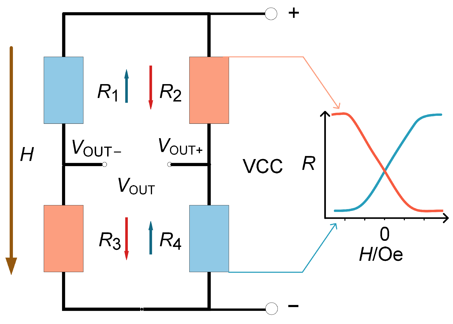
H are the variations in magnetoresistance and magnetic field, respectively. If we consider the Wheatstone bridge structure shown in
Figure 1 as the output of the TMR, the output results are as shown as (1).
where
VCC is the supply voltage,
represents the resistance in
Figure 1 when
is at its maximum, and
represents the resistance when
is at its minimum.
Assume that the resistance of the TMR varies linearly and has a continuously near-zero magnetic field. Besides, under an applied magnetic field, the increase and decrease in resistance of adjacent arms of the Wheatstone bridge structure are equal. (1) can reach the sensitivity of the TMR sensors expressed as (2).
where
represents the change in resistance within the linear magnetic field range
and
is the average resistance between the maximum and minimum resistances in the linear range of the TMR.
According to (2), the sensitivity of the TMR sensor is determined by the linear magnetic field range and the ratio of resistance change. Sensitivity can be enhanced by increasing the ratio of resistance change and reducing the magnetic field range.
The noise level of TMR,
, also determines the measurement capability of the magnetic field sensor. It mainly consists of thermal noise (
), shot noise (
), electrical noise (
), and magnetic noise (
), and can be expressed as (3).
Among these noises, thermal noise is the intrinsic noise of electronic devices and is difficult to reduce, usually serving as the fundamental limiting factor of the device. Electrical 1/
f noise and magnetic 1/
f noise are frequency-dependent and are the primary limiting factors in low-frequency signal measurements. Based on the empirical Hooge constant [
9,
18,
32], the frequency-dependent components of electrical noise and magnetic noise can be expressed as (4).
where
is the Hooge constants for the electrical and
is the normalized 1/
f magnetic noise parameter (Hooge-like).
is the current flowing through the TMR,
the resistance of the TMR,
A is the MTJ area of the TMR, and
f is the frequency of the signal being measured.
is the saturation field of free layer.
is the volume of free layer. This formula indicates that there exist noises in TMR that are similar to the noise in electronic conduction systems and can be characterized by a Hooge-like parameter.
However, considering noise and sensitivity as two independent parameters is insufficient to directly assess the measurement capability of the Wheatstone-bridge-structured TMR. The detection (
) of the TMR is defined as (5).
In applications involving weak magnetic field measurements, higher sensitivity is desired, while low noise is also crucial. Therefore, designing device parameters and obtaining optimized device parameters are necessary in the preparation of TMR sensors.
2.2. Sensitivity Analysis Based on the Stoner–Wohlfarth Model
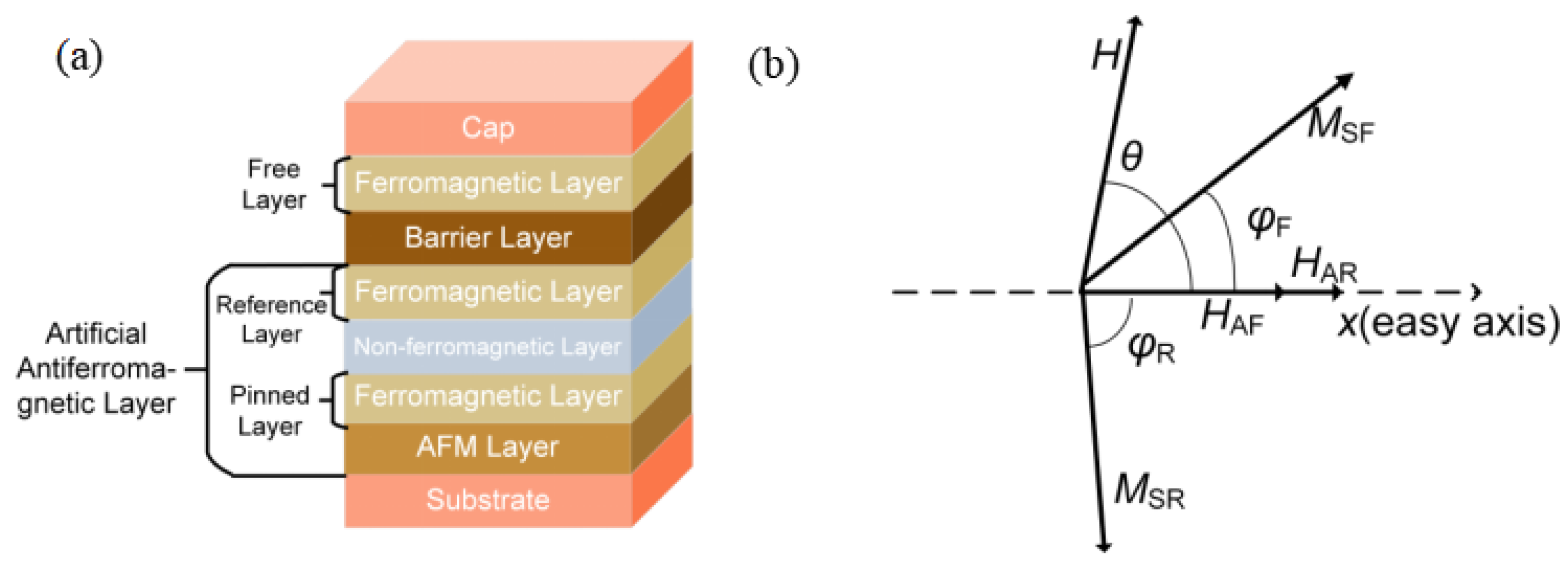
The core structure of the linear TMR sensor consists of an antiferromagnetic layer/ferromagnetic layer/non-magnetic metal layer/ferromagnetic layer/barrier layer/ ferromagnetic layer, as shown in
Figure 2a. The magnetic moments of the two ferromagnetic layers adjacent to the antiferromagnetic (AFM) layer are fixed in the hard axis direction under the action of the exchange bias field. The magnetic moment of the free layer is free to rotate with the applied magnetic field.
The angular difference between the directions of the magnetic moments of the free layer () and the reference layer () determines the magnitude of the output magnetic resistance. The MTJ outputs a minimum resistance () when = 0, while the MTJ outputs a maximum resistance () when . The relationship between the output resistance of the linear TMR and the angle between the magnetic moment directions of the reference and free layers is R = RaveRmaxcos()). is the resistance that varies over the range of the magnetic field.
The Stoner–Wohlfarth (S-W) model considers the magnetization reversal behavior of single-domain magnetic particles under an external magnetic field. For TMR sensors, the magnetization of its ferromagnetic layer can be effectively described by the S-W model [
33,
34,
35]. The energy of the S-W model usually considers the free layer, reference layer, and pinned layer. Due to the influence of AFM exchange bias field, the energy of the reference layer and the pinned layer remains almost unchanged under a small magnetic field. Considering only the energy variation in the free layer, a simplified S-W model can be obtained as shown in
Figure 2b, with the coordinate x-axis coinciding with the easy axis of the TMR.
Variable
can be solved according to the steady state energy minimum principle with S-W model. The energy of the free layer (
) primarily consists of Zeeman energy, magnetocrystalline anisotropy energy, and shape anisotropy energy, as expressed in (6).
where
and
are the anisotropy field of free layer and reference layer, respectively, (
) is the direction of the magnetic field,
H is the magnetic field value, and
and
are the magnetic moment of the free layer and reference layer, respectively.
When
reaches a steady state, the magnetization energy of the free layer is minimized. Specifically, when
is fixed, the variable
is determined by
H, satisfying the equality relationship in (7).
Since (7) is a transcendental equation without an analytical solution, numerical methods are required to determine for varying values of H.
2.3. Results of Sensitivity Simulation Based on the S-W Model
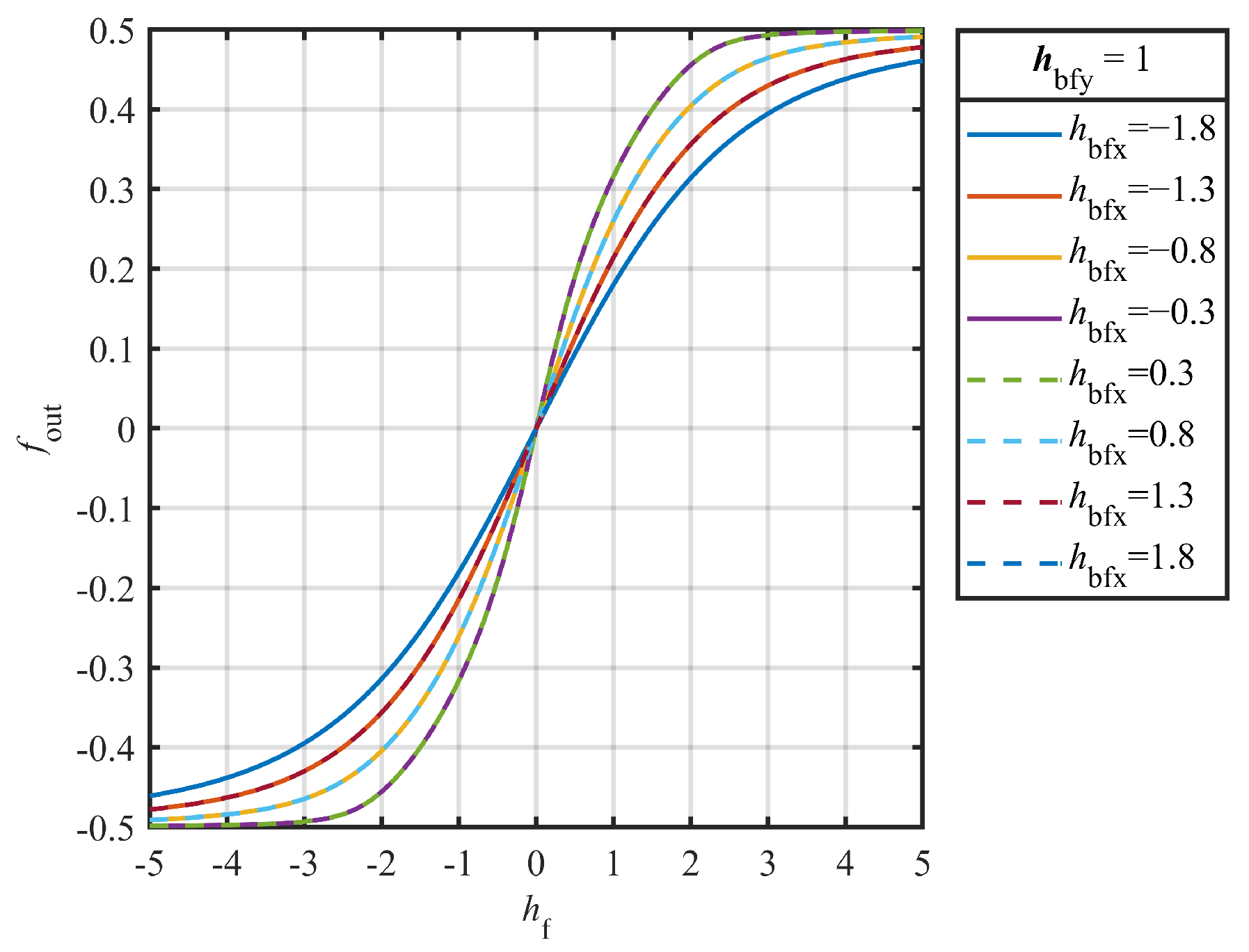
Consider three structural parameters of the TMR: the long-axis lengths of the TMR, the annealing parameters, and the magnetic field bias along the easy axis (). The first two parameters are implicit, and their effects on the sensitivity of the TMR cannot be directly analyzed from the S-W model. However, these can be incorporated into the , allowing the overall impact of the bias to be analyzed using the S-W model.
Assuming that the TMR constituting each bridge arm have good symmetry, the response of the resistance to the magnetic field is opposite in sign and equal in amplitude in the linear range. The transfer function of the output voltage with respect to the angle of clamping as shown in (8) can be obtained.
In this case, represents the normalized output voltage relative to the supply voltage. and represent the magnetic moment directions of the free layer and reference layer for the TMR and , while and represent the magnetic moment directions of the free layer and reference layer for the TMR and .
As shown in
Figure 3, the normalized value of magnetic field bias along the easy axis
affects the sensitivity of the TMR. Sensitivity decreases as
increases, which is reflected by a reduced slope in the graph. Moreover, the symbol
does not affect the sensitivity. This is represented in the graph by the overlap of the output curve for equal-magnitude positive and negative biases along the easy axis. As the overall bias strength along the easy axis increases, the sensitivity of the TMR decreases. Therefore, to improve TMR sensitivity, the |
| should be minimized during the fabrication process. The artificial AFM structure consists of a multilayered MnIr/CoFe/Ru/CoFe/CoFeB films, where the CoFeB layer serves as the reference layer and is antiferromagnetically coupled with the CoFe layer via the non-metallic Ru layer, fixing its magnetic moment along the hard axis. The barrier layer consists of MgO with a <001> orientation. CoFeB on the other side of the MgO constitutes the free layer, whose magnetic moment direction is free to rotate.
4. Result and Discussion
4.1. Experimental Results of TMR Wafer Resistance Sensitivity
Measure the magnetic field response of a TMR wafer resistance. A magnetic field was applied to the TMR in a magnetically shielded chamber to measure the response of the TMR to changes in magnetic field. The magnetic field generated by the electromagnet was calibrated by a Gaussmeter (LakeShore Model 425) to obtain a highly accurate magnetic field–current relationship. The current flowing through the TMR wafer was measured by applying a 1 V voltage to both ends of the TMR wafer through the source meter (Agilent 2912B model) to obtain the resistance value of the TMR wafer at different magnetic fields to obtain the sensitivity of the TMR wafer.
The MR performance of different number of series connections is measured at room temperature, and the annealing magnetic field is 6.5 kOe for TMR device. As an example, the MR at different numbers of series connections is shown in
Table 1. TMR with a 64 μm long-axis length cannot achieve more than 128 series connections in a limited area (1200 × 600 μm
2). Therefore, when the number of series connections exceeds 128, the number of MTJ in 64 μm long-axis length TMR is 192 (two resistors per cell) and 384 (one resistor per cell).
After deposition of the TMR thin layer, the MR was measured directly using a probe and was up to 120.2%. When the number of series connections is less than 64, the resistance of the electrodes used for series connections accounts for a large proportion of the TMR, resulting in an MR much less than the nominal value of 120%. When the number of series connections is greater than 128, the MR increases slightly with the number of series connections and stabilizes above 60%. The number of series connections affects the grain size, which affects the total size of the TMR sensor. Considering that the MR tends to stabilize for TMR series number of 128 and above, 128 or 256 series number was chosen as the design series number for TMR to achieve a larger TMR ratio while the total sensor size is smaller.
TMR devices were prepared under different annealing parameters and the measured results are shown in
Figure 5a,b. The curve labeled “0 kOe” represents the unannealed test results, while the other curve corresponds to the results after two annealing steps with different
.
The variation of
(
Figure 5b) shows that the process is unable to fix the direction of the magnetic moment of the reference layer completely on the hard axis when the
is low (e.g., 2 kOe). On the other hand, if the
is too high (e.g., 8 kOe), the MR deteriorates. There exists an optimal value of the
to maximize the MR. Specifically, in this study, the MR reaches its highest value with
of 6.5 kOe, at which time the sensitivity is maximized.
The effect of long-axis length on the TMR as well as the sensitivity of the TMR wafer is tested for the TMR device parameters with 128 series number, as shown in
Figure 5c. The MR of the TMR decreases with the increase of the long-axis length, and
Figure 5d illustrates that the MR of the TMR decreases nearly linearly with the increase of the long-axis length. Linear fitting of the rising and falling segments of the TMR is performed separately, and the results are shown in
Figure 5e. When the long-axis length of the TMR device increases, the sensitivity
S decreases. At a long-axis length of 8 μm, a decrease in the slope of the
S is observed from the fitted curve in
Figure 5e. At the same time, the increase in the long-axis length will reduce the hysteresis of the TMR (in
Figure 5c), which is about 20 Oe when the long-axis length is 4 μm and about 10 Oe when the long-axis length reaches 64 μm. However, the hysteresis cannot be reduced to 0 by changing the long-axis length of the TMR, and therefore, other options need to be considered to regulate the hysteresis.
The
will also affect the performance of the sensitivity of the TMR, and the test to analyze the effect of the
on the sensitivity level is shown in
Figure 5f,g. When
is different, the output sensitivity of the TMR with the magnetic field in the direction of the difficult axis will change, and it reaches the maximum value when the bias is at the level of −12.19 Oe. Analytical fitting of the change in sensitivity yields the results shown in
Figure 5h. That is, there exists an optimal result for the sensitivity of the TMR with the bias, and the fitting equation is shown in (9).
where the fitting equation has a goodness-of-fit of 0.9916, and the parameters are
a1 = 26.68,
a0 = 410.2,
b1 = −1.336,
b0 = 842.5, and
c = 0.09661. The sensitivity of the TMR is symmetric about the
HBFX of about −12 Oe, and it decreases with the increase in the difference between
HBFX with the symmetry line of the
HBFX, with an approximate tends to be an inversely proportional function.
4.2. TMR Wafer Hysteresis
The TMR device formed by using the two-step annealing process alone has a large hysteresis, which affects the output results of the TMR. According to the results in
Section 4.1, the effect of hysteresis cannot be eliminated by changing the annealing parameters and the long-axis lengths of the TMR. Modulating the
HBFX will reduce the hysteresis. Considering the effect of different
HBFX on the hysteresis, the hysteresis optimizing results are obtained as shown in
Figure 5i.
Obtain the hysteresis of TMR from the test data and evaluate it using the following methods. TMR hysteresis is only meaningful within a linear range. Linearly fit the TMR resistance output curve of the upward and downward segments separately to obtain the fitting functions of the two branches. Based on this sensitivity, calculate the magnetic field difference between the two branches when they reach the same Rave. This difference value is used as the hysteresis of TMR for evaluation.
The hysteresis of the TMR reaches a level of less than 1 Oe when the HBFX is more than −40 Oe in the negative direction or more than 17 Oe in the positive direction. The hysteresis curve exhibits similar angular characteristics at different angles of the external field, with a relatively smaller level of hysteresis at 90° external field.
4.3. Wheatstone Bridge Structure TMR Sensitivity Results
Furthermore, the TMR devices were configured into a Wheatstone bridge structure, as shown in
Figure 1. The packaged device is shown in
Figure 6a. Two TMR cells were mounted in opposite orientations on a PCB board, with the sensitive axes of the resistances in the two TMR chips aligned in opposite directions. Gold wires were used to connect the corresponding pins of the TMR, resulting in a packaged bridge-type TMR sensor.
To assess the impact of
HBFX on the TMR output response, a series of magnetic fields bias with varying intensities were applied along the easy axis of the TMR using a biaxial Helmholtz coil. The output response was then precisely measured and recorded as the magnetic field along the hard axis was varied. Testing was conducted on a TMR sensor with 128 series connections and
kOe. Typical test results are shown in
Figure 6b,c display the output curve corresponding to long-axis lengths of 4 μm and 16 μm, respectively.
After applying
, a significant reduction in hysteresis was observed for the TMR device through
Figure 6b,c. Clear linear regions appeared in the output curve for bias fields greater than 37 Oe. The fitted sensitivity of the TMR resistance output curve for the measured magnetic field variations is summarized in
Table 2 and
Table 3.
Table 2 presents the sensitivity fitting results for the magnetic field decreasing process, while
Table 3 shows the results for the magnetic field increasing process. At lower bias levels, as illustrated in
Figure 6b,c, the presence of substantial hysteresis and discontinuities in the linear region means that the fitted sensitivity may not accurately reflect the TMR’s measurement capability. This discrepancy is evident in the significant difference between the sensitivity fitting results for increasing and decreasing fields. When the sensitivity fitting results for the increasing and decreasing processes differ by less than 1%, hysteresis effects are considered negligible. There exists an ideal linear range, only in where the sensitivity is meaningful. Therefore, we select the maximum sensitivity that differs by less than 1% under the same configuration from two tables as the optimal sensitivity.
For TMR sensors with a long-axis length of 64 μm, a relatively high HBFX = 52.23 Oe is required to achieve a reasonable linear region, resulting in a sensitivity of only 55.8 V/V/T. As the long-axis length of the TMR sensor decreases, sensitivity improves, and the required HBFX also decreases. For instance, TMR sensors with long-axis length ranging from 16 μm to 4 μm require HBFX = 47.24 Oe to meet the 1% sensitivity error criterion, with maximum sensitivity reaching 112.88 V/V/T at a long-axis length of 4 μm.
Analyzing with the HBFX, for the same long-axis-length sensor, increasing the HBFX reduces the hysteresis and enhances the linearity, but the sensitivity decreases as the HBFX increases. For the TMR sensors prepared in this paper, the best parameters for sensitivity are 128 series, 4 μm long-axis length, , and HBFX for the TMR sensors.
4.4. Measurement of Noise Levels
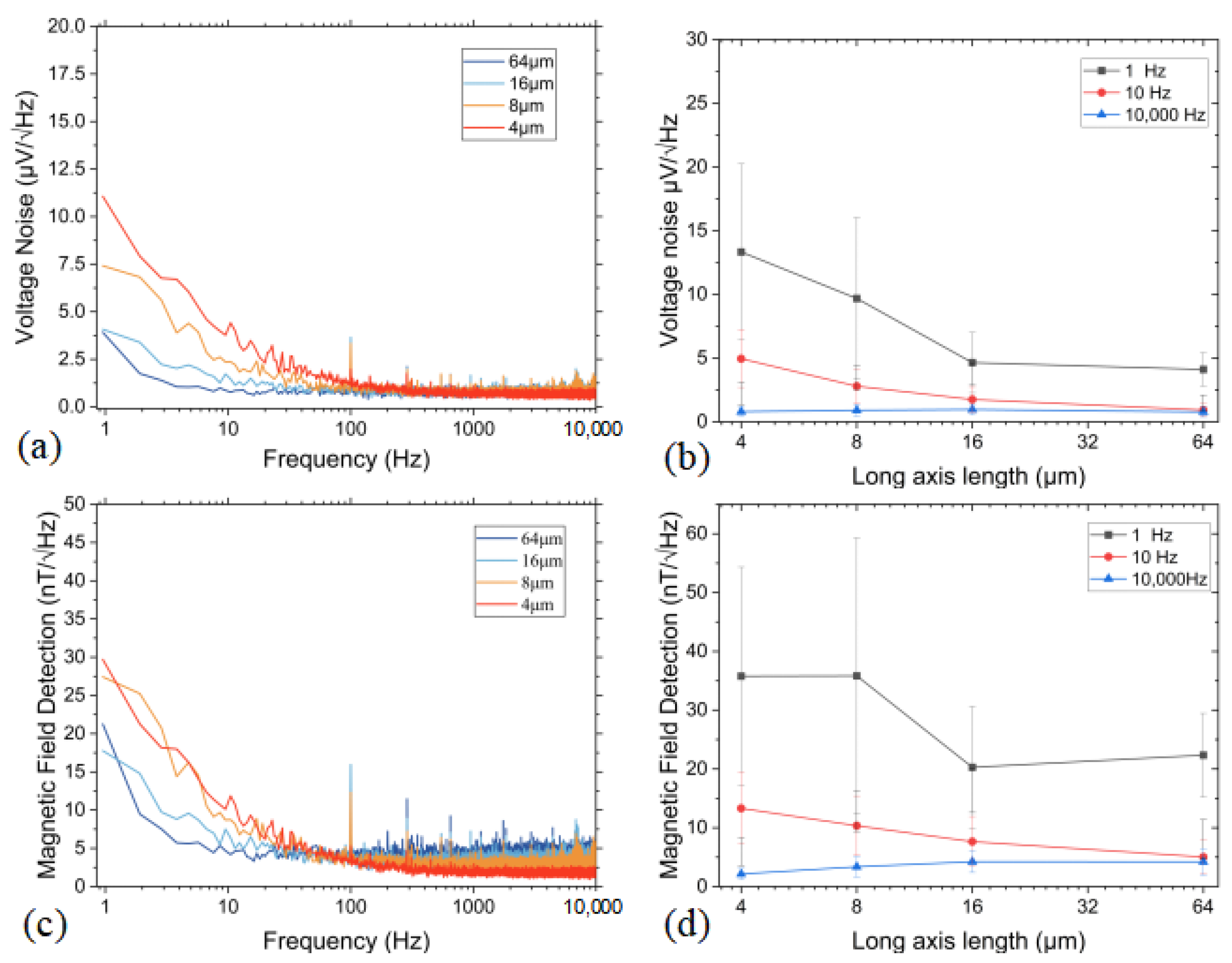
To evaluate the output noise characteristics of the TMR Wheatstone bridge structure, a systematic data processing procedure was implemented. Specifically, we first applied a Fourier transform to the acquired noise signals, followed by averaging the data 20 times to analyze the spectral characteristics of the noise.
We selected a TMR sensor with a number of 128 series MTJ connections as a test subject and investigated the effect of the variable of long-axis length on its noise performance. Through precise measurements and analysis, the corresponding results were obtained, as shown in
Figure 7a. From the analysis, it is evident that as the long-axis length of the TMR decreases, the low-frequency voltage noise level also decreases. When the long-axis length is reduced to 4 μm, the low-frequency voltage noise level reaches the 10 μV. However, when the long-axis length increases to 16 μm, the low-frequency voltage noise level drops to around 4 μV. Combined with the sensitivity analysis in
Section 4.3, the magnetic field noise level was derived, as shown in
Figure 7b.
For devices with long-axis lengths of 64 μm and 16 μm, sensitivity was measured under a magnetic field bias of 52.32 Oe, resulting in sensitivities of 55.81 V/V/T and 69.43 V/V/T, respectively. For devices with long-axis lengths of 8 μm and 4 μm, sensitivity was measured under a magnetic field bias of 47.21 Oe, yielding sensitivities of 81.88 V/V/T and 112.88 V/V/T, respectively. Considering that the supply voltage for measuring TMR voltage noise comes from a low-noise 3.3 V battery, it is important to ensure that the equivalent supply voltages are consistent, when calculating the magnetic field noise based on the voltage noise and sensitivity.
At a frequency of 1 Hz, the device with a long-axis length of 16 μm exhibited the best magnetic field detection, with a value of 17.7 nT/V/
@1Hz, as shown in
Figure 7c (light blue line). Compared to the other points in
Figure 7d, the long-axis lengths of 16 μm and 64 μm exhibit better performance at low frequencies. For noise measurement, the main source of error are white noise and randomness. In the statistics of the error bars, the standard deviation of the noise is approximately between 30% and 50%. This parameter combination produced a TMR sensor with improved magnetic field measurement capabilities, offering the potential for weak magnetic field detection.
5. Conclusions
In this research, we fabricated and characterized a series of MTJs with elliptical cross-sections and varying long-axis lengths. We investigated the effects of series connections, long-axis lengths, annealing magnetic fields, and bias magnetic field parameters on TMR sensitivity, as well as the impact of long-axis lengths on noise. The TMR transmission curve demonstrated that TMR sensitivity is closely related to size parameters. Sensors with elliptical free layers and smaller MTJ areas exhibited extremely high sensitivity. Furthermore, increasing the long-axis lengths significantly reduced the voltage noise power in the low-frequency region. Considering the overall detection, TMR devices with a long-axis length of 16 μm achieved superior magnetic field detection capability, which is consistent with the predicted results, reaching a detection level in the 17.7 nT/@1Hz.
In terms of series connections, TMR sensors with a higher number of series junctions exhibited greater stability and sensitivity. Selecting 128 or more series connections as the TMR configuration parameter allows for the development of highly sensitive sensors.
Excessively high annealing magnetic fields can degrade the crystalline structure, thereby reducing TMR sensitivity, while excessively low annealing fields fail to pin the reference layer in the hard axis direction, also leading to reduced sensitivity. In this research, an annealing magnetic field of 6.5 kOe was selected to optimize TMR sensitivity.
The can eliminate the hysteresis effect in TMR; however, a high bias reduces sensitivity. Thus, a bias magnetic field of 47.24 Oe was chosen to maximize sensitivity while keeping hysteresis within a reasonable range.
Experimental results indicate that the long-axis lengths of the TMR plays a crucial role in detecting magnetic field variations, while the number of series junctions and the annealing magnetic field primarily influence the stability of the TMR, with only minor effects on sensitivity. These results provide significant guidance for the optimization of TMR sensors design, particularly in the design of the high-sensitivity and low-noise TMR sensors.


