Large-Area Nanostructure Fabrication with a 75 nm Half-Pitch Using Deep-UV Flat-Top Laser Interference Lithography
Abstract
1. Introduction
2. Experimental Methods
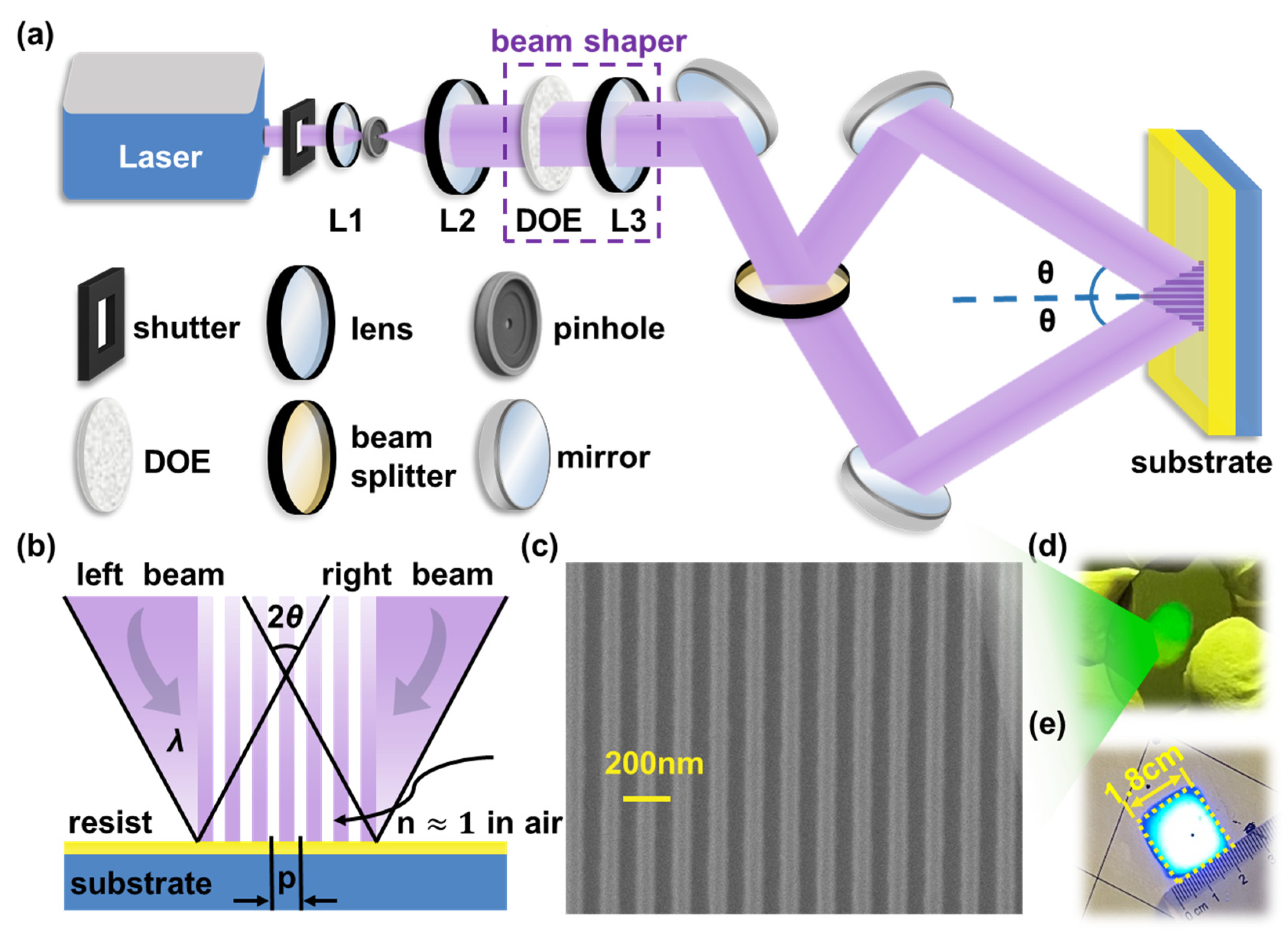
2.1. Experimental Principle
2.1.1. Period Control and Design Tradeoffs
2.1.2. Determinants of Duty Cycle and Dose Measurement
2.2. Experimental Setup
2.3. Wafer Preparation, Exposure, and Development
3. Results
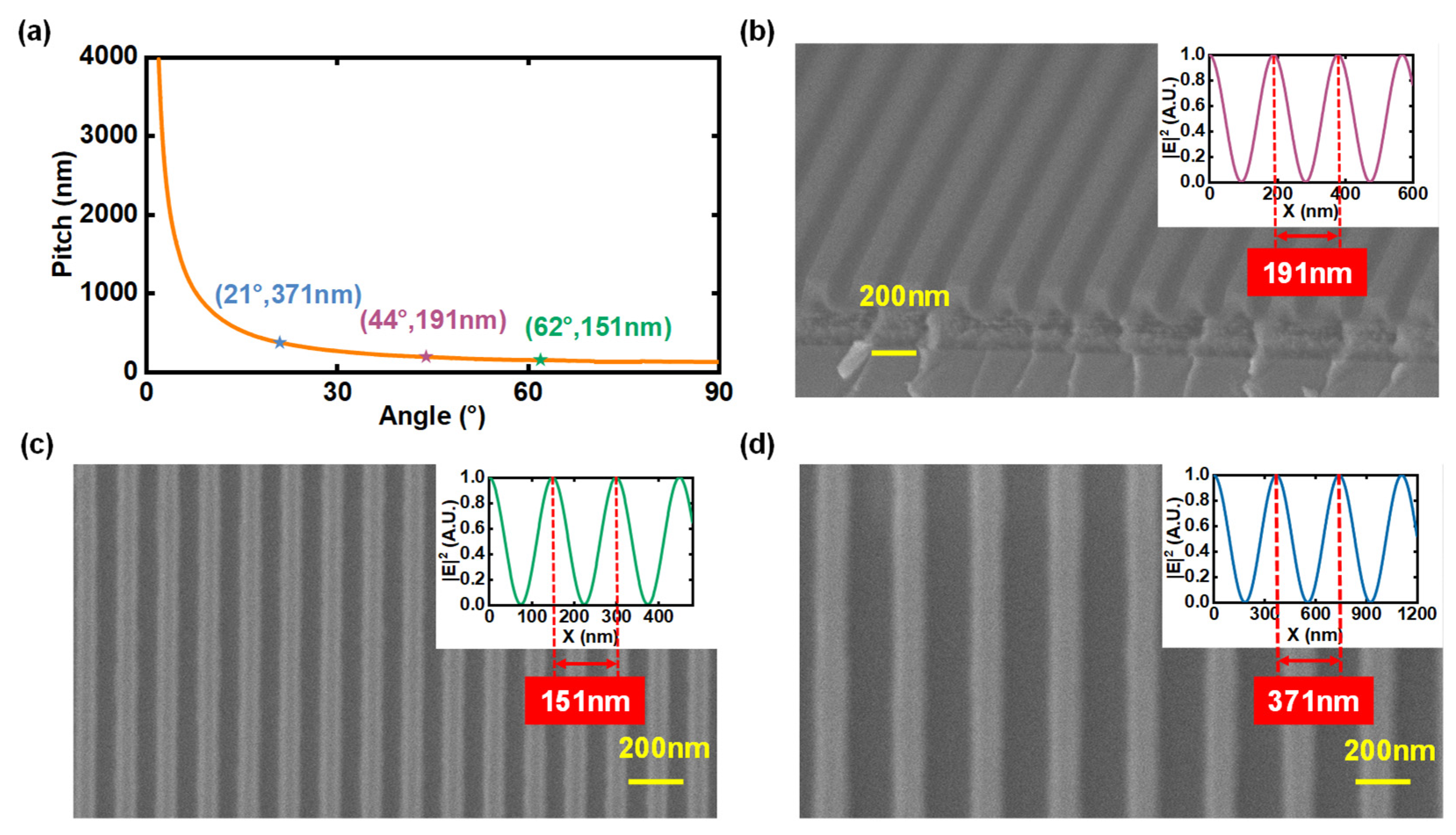
3.1. Angle-Tuned Pitch Scaling for Large-Area 150 nm Patterns
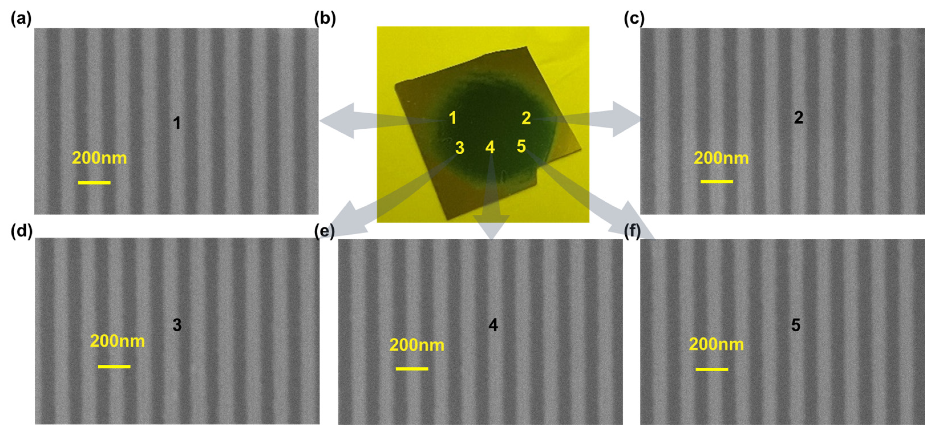
3.2. Uniformity Verification of Centimeter-Scale Grating Pattern
3.3. SERS-Based Uniformity Assessment of Nanodot Arrays
4. Discussion
5. Conclusions
- Deep-ultraviolet period setting with a moderate angle. Using a 266 nm source and a moderate incidence half-angle, we realize 75 nm half-pitch while preserving a large beam-overlap region and stable alignment. At this wavelength the chosen angle delivers a 150 nm period with robust field coverage rather than relying on extreme angles that shrink the usable overlap.
- Flat-top illumination for uniformity and process latitude. A diffractive flat-top shaper combined with a relay lens produces a uniform on-wafer irradiance. Together with a power balance near unity fringe visibility, this yields centimeter-scale uniformity and tight control of duty cycle. We pattern one-dimensional gratings and two-dimensional arrays over a Ø1.0 cm field with critical-dimension variation below 5 nm (1σ), smooth edges, and near-vertical sidewalls.
- Application validation with SERS arrays. We validate utility using silicon-transferred 2D nanodot arrays as SERS substrates, where low signal variation across 65 randomly sampled points (11% RSD) indicates a highly ordered and consistent geometry and addresses the uneven hotspot distribution and complex fabrication procedures common to conventional SERS substrates, with an apparent enhancement factor of ~1.12 × 10⁴.
Author Contributions
Funding
Institutional Review Board Statement
Informed Consent Statement
Data Availability Statement
Conflicts of Interest
Appendix A

References
- Pandey, A.; Maity, S.; Murmu, K.; Middya, S.; Bandyopadhyay, D.; Pattader, P.S.G. Self-organization of random copolymers to nanopatterns by localized e-beam dosing. Nanotechnology 2021, 32, 285302. [Google Scholar] [CrossRef]
- Li, Y.; Hong, M. Parallel Laser Micro/Nano-Processing for Functional Device Fabrication. Laser Photon. Rev. 2020, 14, 1900062. [Google Scholar] [CrossRef]
- Yang, H.; Huang, H.; Liu, X.; Li, Z.; Li, J.; Zhang, D.; Chen, Y.; Liu, J. Sensing mechanism of an Au-TiO2-Ag nanograting based on Fano resonance effects. Appl. Opt. 2023, 62, 4431–4438. [Google Scholar] [CrossRef]
- Du, K.; Wathuthanthri, I.; Choi, C.-H. The Rise of Scalable Micro/Nanopatterning. Micromachines 2017, 8, 275. [Google Scholar] [CrossRef]
- Cao, Q.; Lü, W.; Wang, X.R.; Guan, X.; Wang, L.; Yan, S.; Wu, T.; Wang, X. Nonvolatile Multistates Memories for High-Density Data Storage. ACS Appl. Mater. Interfaces 2020, 12, 42449–42471. [Google Scholar] [CrossRef]
- Song, L.; Yang, D.; Lei, Z.; Sun, Q.; Chen, Z.; Song, Y. A Reflectivity Enhanced 3D Optical Storage Nanostructure Application Based on Direct Laser Writing Lithography. Materials 2023, 16, 2668. [Google Scholar] [CrossRef]
- So, S.; Kim, J.; Badloe, T.; Lee, C.; Yang, Y.; Kang, H.; Rho, J. Multicolor and 3D Holography Generated by Inverse-Designed Single-Cell Metasurfaces. Adv. Mater. 2023, 35, e2208520. [Google Scholar] [CrossRef]
- Zheng, Y.; Liu, H.; Xiang, J.; Dai, Q.; Ouyang, M.; Tie, S.; Lan, S. Hot luminescence from gold nanoflowers and its application in high-density optical data storage. Opt. Express 2017, 25, 9262–9275. [Google Scholar] [CrossRef] [PubMed]
- De Arquer, F.P.G.; Talapin, D.V.; Klimov, V.I.; Arakawa, Y.; Bayer, M.; Sargent, E.H. Semiconductor quantum dots: Technological progress and future challenges. Science 2021, 373, 640. [Google Scholar] [CrossRef] [PubMed]
- Eaton, S.M.; Hadden, J.P.; Bharadwaj, V.; Forneris, J.; Picollo, F.; Bosia, F.; Sotillo, B.; Giakoumaki, A.N.; Jedrkiewicz, O.; Chiappini, A.; et al. Quantum Micro–Nano Devices Fabricated in Diamond by Femtosecond Laser and Ion Irradiation. Adv. Quantum Technol. 2019, 2, 1900006. [Google Scholar] [CrossRef]
- Wang, Y.-R.; Han, I.S.; Hopkinson, M. Fabrication of quantum dot and ring arrays by direct laser interference patterning for nanophotonics. Nanophotonics 2023, 12, 1469–1479. [Google Scholar] [CrossRef]
- Nam, T.W.; Choi, M.-J.; Jung, Y.S. Ultrahigh-resolution quantum dot patterning for advanced optoelectronic devices. Chem. Commun. 2023, 59, 2697–2710. [Google Scholar] [CrossRef] [PubMed]
- Park, S.Y.; Lee, S.; Yang, J.; Kang, M.S. Patterning Quantum Dots via Photolithography: A Review. Adv. Mater. 2023, 35, e2300546. [Google Scholar] [CrossRef]
- Zhou, Y.; Wang, S.; Yin, J.; Wang, J.; Manshaii, F.; Xiao, X.; Zhang, T.; Bao, H.; Jiang, S.; Chen, J. Flexible Metasurfaces for Multifunctional Interfaces. ACS Nano 2024, 18, 2685–2707. [Google Scholar] [CrossRef]
- Park, J.-S.; Lim, S.W.D.; Amirzhan, A.; Kang, H.; Karrfalt, K.; Kim, D.; Leger, J.; Urbas, A.; Ossiander, M.; Li, Z.; et al. All-Glass 100 mm Diameter Visible Metalens for Imaging the Cosmos. ACS Nano 2024, 18, 3187–3198. [Google Scholar] [CrossRef]
- Zhuang, X.; Zhang, W.; Wang, K.; Gu, Y.; An, Y.; Zhang, X.; Gu, J.; Luo, D.; Han, J.; Zhang, W. Active terahertz beam steering based on mechanical deformation of liquid crystal elastomer metasurface. Light Sci. Appl. 2023, 12, 14. [Google Scholar] [CrossRef]
- Dey, R.K.; Cui, B. Electron beam lithography with feedback using in situ self-developed resist. Nanoscale Res. Lett. 2014, 9, 184. [Google Scholar] [CrossRef]
- Khodadad, I.; Nelson-Fitzpatrick, N.; Burcham, K.; Hajian, A.; Saini, S.S. Electron beam lithography using fixed beam moving stage. J. Vac. Sci. Technol. B 2017, 35, 051601. [Google Scholar] [CrossRef]
- Fourkas, J.T.; Gao, J.; Han, Z.; Liu, H.; Marmiroli, B.; Naughton, M.J.; Petersen, J.S.; Sun, Y.; Pret, A.V.; Zheng, Y. Grand Challenges in Nanofabrication: There Remains Plenty of Room at the Bottom. Front. Nanotechnol. 2021, 3, 700849. [Google Scholar] [CrossRef]
- Hasan, R.M.M.; Luo, X. Promising Lithography Techniques for Next-Generation Logic Devices. Nanomanuf. Metrol. 2018, 1, 67–81. [Google Scholar] [CrossRef]
- Wu, M.; Liu, J.; He, J.; Chen, X.; Guo, Z. Fabrication of surface microstructures by mask electrolyte jet machining. Int. J. Mach. Tools Manuf. 2020, 148, 103471. [Google Scholar] [CrossRef]
- Wu, M.; Arshad, M.H.; Saxena, K.K.; Reynaerts, D.; Guo, Z.; Liu, J. Experimental and Numerical Investigations on Fabrication of Surface Microstructures Using Mask Electrolyte Jet Machining and Duckbill Nozzle. J. Manuf. Sci. Eng. 2023, 145, 051006. [Google Scholar] [CrossRef]
- González-Colsa, J.; Serrera, G.; Saiz, J.M.; González, F.; Moreno, F.; Albella, P. On the performance of a tunable grating-based high sensitivity unidirectional plasmonic sensor. Opt. Express 2021, 29, 13733–13745. [Google Scholar] [CrossRef]
- Li, X.; Tang, B.; Wu, B.; Hsu, C.; Wang, X. Highly Sensitive Diffraction Grating of Hydrogels as Sensors for Carbon Dioxide Detection. Ind. Eng. Chem. Res. 2021, 60, 4639–4649. [Google Scholar] [CrossRef]
- Fang, H.; Wei, C.; Yang, H.; Zhao, B.; Yuan, L.; Li, J. D-Shaped Photonic Crystal Fiber Plasmonic Sensor Based on Silver-Titanium Dioxide Composite Micro-grating. Plasmonics 2021, 16, 2049–2059. [Google Scholar] [CrossRef]
- Iqbal, T.; Ashfaq, Z.; Afsheen, S.; Ijaz, M.; Khan, M.Y.; Rafique, M.; Nabi, G. Surface-Enhanced Raman Scattering (SERS) on 1D Nano-gratings. Plasmonics 2020, 15, 1053–1059. [Google Scholar] [CrossRef]
- Chen, Z.; Chen, Z.; Feng, K.; Zou, S.; Li, H. Exploring SERS from two-dimensional symmetric gold array fabricated by double exposure laser interference lithography. Opt. Commun. 2022, 514, 128169. [Google Scholar] [CrossRef]
- Wen, X.; Lu, X.; Li, J.; Wei, C.; Qin, H.; Liu, Y.; Yang, S. Multi-responsive, flexible, and structurally colored film based on a 1D diffraction grating structure. iScience 2022, 25, 104157. [Google Scholar] [CrossRef] [PubMed]
- Wang, W.; Guan, Z.; Xu, H. A high speed electrically switching reflective structural color display with large color gamut. Nanoscale 2020, 13, 1164–1171. [Google Scholar] [CrossRef]
- Huo, D.; Li, G. Bi-Directional Full-Color Generation and Tri-Channel Information Encoding Based on a Plasmonic Metasurface. Nanomaterials 2024, 14, 1160. [Google Scholar] [CrossRef]
- Shimizu, Y. Laser Interference Lithography for Fabrication of Planar Scale Gratings for Optical Metrology. Nanomanuf. Metrol. 2021, 4, 3–27. [Google Scholar] [CrossRef]
- Jia, X.; Luo, J.; Li, K.; Wang, C.; Li, Z.; Wang, M.; Jiang, Z.; Veiko, V.P.; Duan, J. Ultrafast laser welding of transparent materials: From principles to applications. Int. J. Extreme Manuf. 2025, 7, 032001. [Google Scholar] [CrossRef]
- Luo, Y.; Fang, L.-N.; Wei, W.-H.; Guan, W.; Dai, Y.-Z.; Sun, X.-C.; Gao, B.-R. Shape memory of a polymer grating surface fabricated by two-beam interference lithography. Appl. Opt. 2022, 61, 792–796. [Google Scholar] [CrossRef]
- Liu, T.; Wang, S.; Li, T.; Wang, G.; Dong, L.; Zhang, W.; Qiao, J.; Xu, H.; Wang, Z.; Weng, Z. Soft lithography for flexible structural color films by laser interference lithography. Opt. Laser Technol. 2024, 181, 111689. [Google Scholar] [CrossRef]
- Liu, R.; Cao, L.; Liu, D.; Wang, L.; Saeed, S.; Wang, Z. Laser Interference Lithography—A Method for the Fabrication of Controlled Periodic Structures. Nanomaterials 2023, 13, 1818. [Google Scholar] [CrossRef]
- Wang, S.; Xu, X.; Jia, X.; Ding, Y.; Gao, Z.; Jiang, X.; Wang, C. Convex silica microlens arrays processed by a Bessel beam femtosecond laser. Opt. Lett. 2025, 50, 4470–4473. [Google Scholar] [CrossRef]
- Bienert, F.; Röcker, C.; Graf, T.; Ahmed, M.A. Bending of Lloyd’s mirror to eliminate the period chirp in the fabrication of diffraction gratings. Opt. Express 2024, 32, 18430–18440. [Google Scholar] [CrossRef]
- Xue, G.; Lu, H.; Li, X.; Zhou, Q.; Wu, G.; Wang, X.; Zhai, Q.; Ni, K. Patterning nanoscale crossed grating with high uniformity by using two-axis Lloyd’s mirrors based interference lithography. Opt. Express 2020, 28, 2179–2191. [Google Scholar] [CrossRef]
- Byun, I.; Kim, J. Cost-effective laser interference lithography using a 405 nm AlInGaN semiconductor laser. J. Micromech. Microeng. 2010, 20, 055024. [Google Scholar] [CrossRef]
- Park, E.-M.; Choi, J.; Kang, B.H.; Dong, K.-Y.; Park, Y.; Song, I.S.; Ju, B.-K. Investigation of the effects of bottom anti-reflective coating on nanoscale patterns by laser interference lithography. Thin Solid Films 2011, 519, 4220–4224. [Google Scholar] [CrossRef]
- Ushkov, A.; Verrier, I.; Kämpfe, T.; Jourlin, Y. Subwavelength diffraction gratings with macroscopic moiré patterns generated via laser interference lithography. Opt. Express 2020, 28, 16453–16468. [Google Scholar] [CrossRef]
- Miller, D.B.; Jones, A.; McLeod, R.R. Contrast analysis in two-beam laser interference lithography. Appl. Opt. 2020, 59, 5399–5407. [Google Scholar] [CrossRef]
- Liu, D.; Liu, R.; Cao, L.; Saeed, S.; Bryanston-Cross, P.J.; Wang, Z. Fabrication of periodic hierarchical structures with anti-icing performance by direct laser interference lithography and hydrothermal treatment. Surf. Coatings Technol. 2023, 471, 129819. [Google Scholar] [CrossRef]
- Xie, Q.; Hong, M.; Tan, H.; Chen, G.; Shi, L.; Chong, T. Fabrication of nanostructures with laser interference lithography. J. Alloys Compd. 2008, 449, 261–264. [Google Scholar] [CrossRef]
- Dai, L.; Xuan, M.; Ding, P.; Jiang, Y.; Ma, Z.; Jia, H.; Wang, W.; Zhou, J.; Chen, H. A novel method to reduce the period limitation in laser interference lithography. Opt. Quantum Electron. 2015, 47, 2331–2338. [Google Scholar] [CrossRef]
- Sasidharan, V.; Neumann, A.; Brueck, S.R.J. Diffraction-grating beam splitter, interferometric-lithography nanopatterning with a multilongitudinal-mode diode laser. J. Vac. Sci. Technol. B 2021, 39, 062603. [Google Scholar] [CrossRef]
- Kim, H.; Kim, D.; Lee, C.; Kim, J. Laser interference lithography using spray/spin photoresist development method for consistent periodic nanostructures. Curr. Appl. Phys. 2014, 14, 209–214. [Google Scholar] [CrossRef]
- Hassanzadeh, A.; Mohammadnezhad, M.; Mittler, S. Multiexposure laser interference lithography. J. Nanophotonics 2015, 9, 093067. [Google Scholar] [CrossRef]
- Mack, C.A.; Jug, S.; Legband, D.A. Data Analysis for Photolithography. Proc. Metrol. Spection Process Control Microlithogr. SPIE 1999, 3677, 415–434. [Google Scholar]
- Zhang, C.; Yi, P.; Peng, L.; Lai, X.; Chen, J.; Huang, M.; Ni, J. Continuous fabrication of nanostructure arrays for flexible surface enhanced Raman scattering substrate. Sci. Rep. 2017, 7, 39814. [Google Scholar] [CrossRef] [PubMed]


| Method | Wavelength (nm) | Pattern Type | Resolution (Pitch, nm) | Area | Ref. |
|---|---|---|---|---|---|
| Two-beam laser interferometer | 266 | Grating/Dot array/hole array | 150 | Ø1.0 cm | This paper |
| Two-beam laser interferometer | 422 | Grating | 600 | 1 µm × 1 µm | [41] |
| Two-beam laser interferometer | 1064 | Grating | 15,000 | -- | [43] |
| Lloyd’s mirror interferometer | 257 | Grating | 770 | 3 cm × 3 cm | [40] |
| Lloyd’s mirror interferometer | 325 | Dot Array | 478 | Centimeter scale | [44] |
| Lloyd’s mirror interferometer | 325 | Grating | 250 | -- | [45] |
| Lloyd’s mirror interferometer | 355 | Grating | 600 | -- | [46] |
| Lloyd’s mirror interferometer | 405 | Grating | 500 | -- | [47] |
| Lloyd’s mirror interferometer | 405 | Grating/Dot Array | 290 | 2 cm × 2 cm | [39] |
| Lloyd’s mirror interferometer | 442 | Grating/Dot Array | 1304 | -- | [48] |
| Lloyd’s mirror interferometer | 785 | Grating | 570 | -- | [27] |
Disclaimer/Publisher’s Note: The statements, opinions and data contained in all publications are solely those of the individual author(s) and contributor(s) and not of MDPI and/or the editor(s). MDPI and/or the editor(s) disclaim responsibility for any injury to people or property resulting from any ideas, methods, instructions or products referred to in the content. |
© 2025 by the authors. Licensee MDPI, Basel, Switzerland. This article is an open access article distributed under the terms and conditions of the Creative Commons Attribution (CC BY) license (https://creativecommons.org/licenses/by/4.0/).
Share and Cite
Jiang, K.; Xie, M.; Tang, Z.; Zhang, X.; Yang, D. Large-Area Nanostructure Fabrication with a 75 nm Half-Pitch Using Deep-UV Flat-Top Laser Interference Lithography. Sensors 2025, 25, 5906. https://doi.org/10.3390/s25185906
Jiang K, Xie M, Tang Z, Zhang X, Yang D. Large-Area Nanostructure Fabrication with a 75 nm Half-Pitch Using Deep-UV Flat-Top Laser Interference Lithography. Sensors. 2025; 25(18):5906. https://doi.org/10.3390/s25185906
Chicago/Turabian StyleJiang, Kexin, Mingliang Xie, Zhe Tang, Xiren Zhang, and Dongxu Yang. 2025. "Large-Area Nanostructure Fabrication with a 75 nm Half-Pitch Using Deep-UV Flat-Top Laser Interference Lithography" Sensors 25, no. 18: 5906. https://doi.org/10.3390/s25185906
APA StyleJiang, K., Xie, M., Tang, Z., Zhang, X., & Yang, D. (2025). Large-Area Nanostructure Fabrication with a 75 nm Half-Pitch Using Deep-UV Flat-Top Laser Interference Lithography. Sensors, 25(18), 5906. https://doi.org/10.3390/s25185906


