

A New Prospective Solution to Meet the New Specifications Required on Agile Beam Antennas: ARMA Theory and Applications

Abstract
Highlights
- A more precise solution than phased arrays that pushes their main limits in all areas: surface efficiency, bandwidth, beam forming, beam steering, conformation, multifunctionality, focusing…
- New applications in terrestrial telecom (IoT, sensors, 5G, 6G…) and space ones (example: CubeSat), but also those in radar and electronic warfare (EW), require new performances for low-profile (LP) beam-agile antennas based on the points described in the previous paragraph.
Abstract
1. Introduction
2. Theory
2.1. Theory Introduction
- It is first derived from Maxwell’s equations, which give the far-field expression E(P) generated by surface currents J(M) located on a radiating surface S (Figure 1), as follows:
- Second, by applying the equivalent principle, it makes the field rigorously radiated to infinity E(P) by any antenna via the surface fields Es evaluated on any closed surface Sc (Figure 2) surrounding the antenna.
2.2. Beam Agility
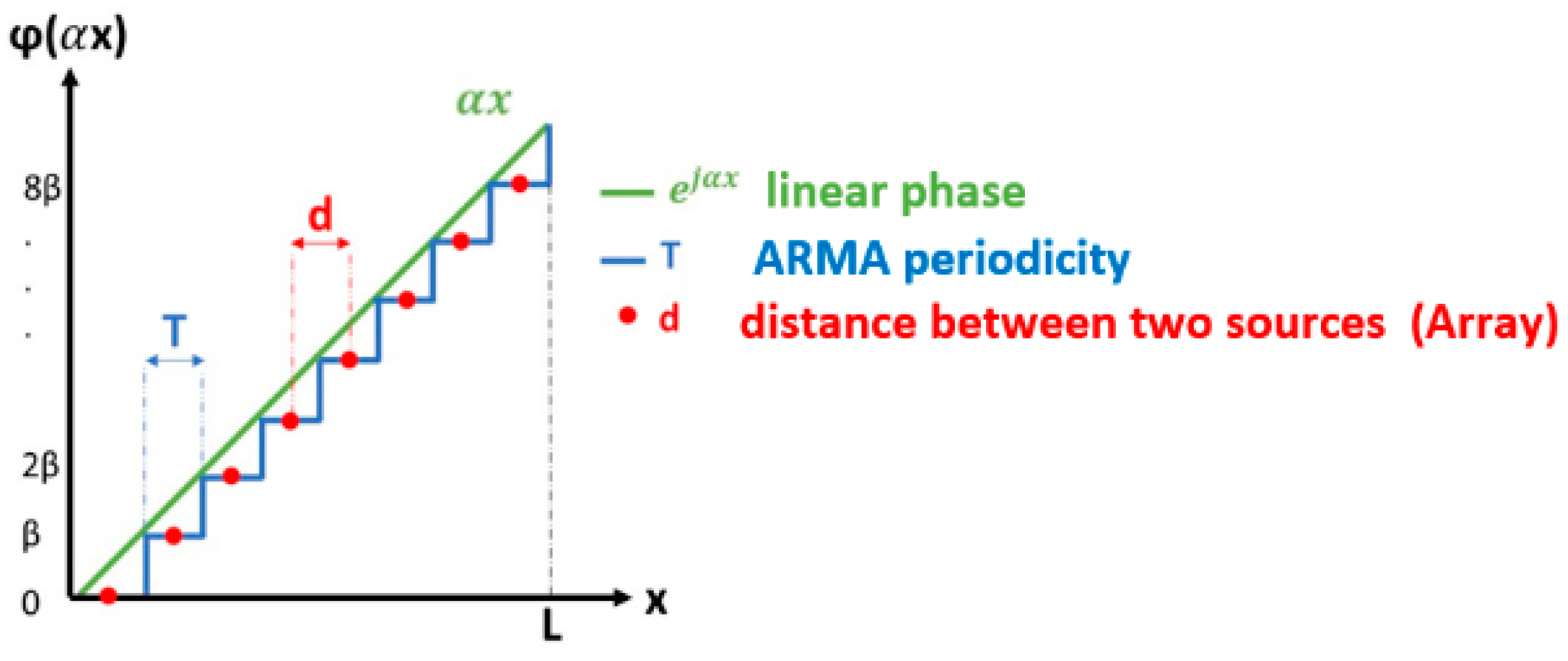
- The first one multiplies in the integral (Equation (4)) by a Dirac comb [6] and leads to the well-known array technique [7] (Equation (7)). The radiated field appears as the sum of the radiations from point sources periodically distributed on the surface S. To physically represent these point sources, patches, slots, and dipoles are used, forming an array of elementary antennas.
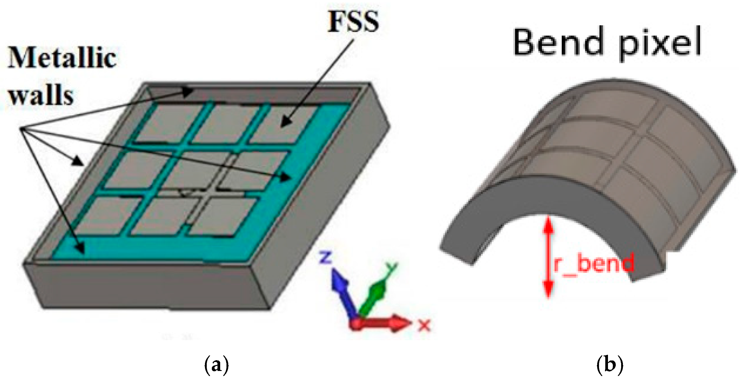
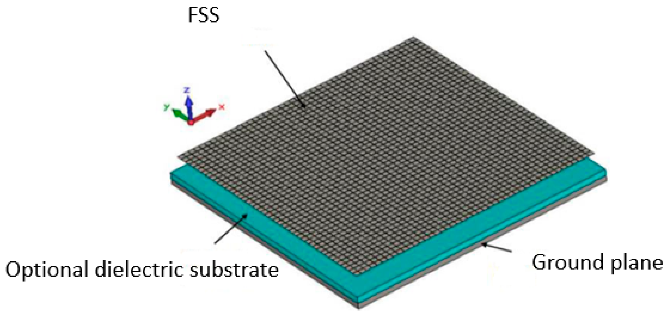
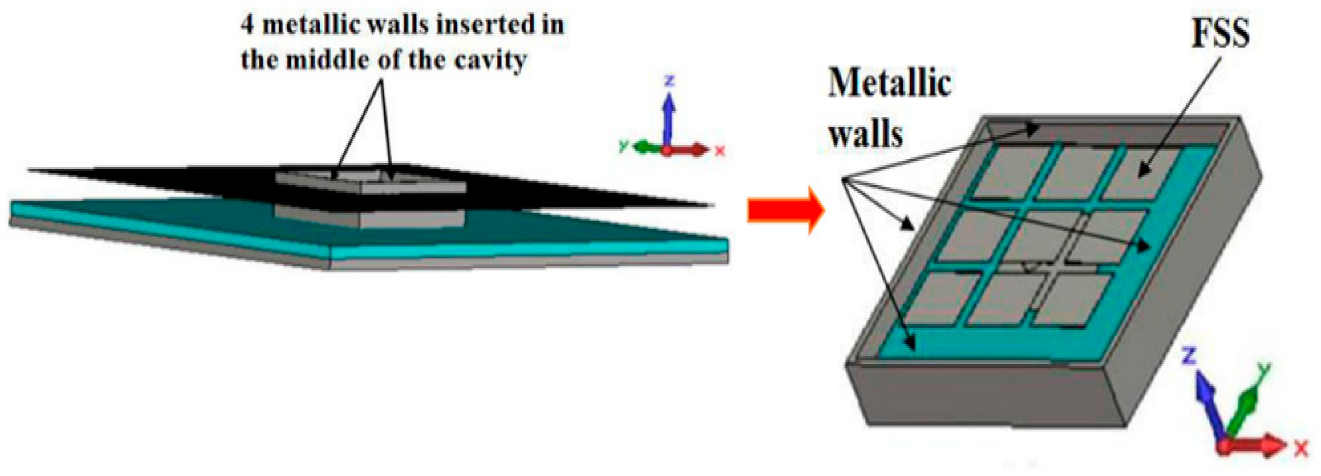
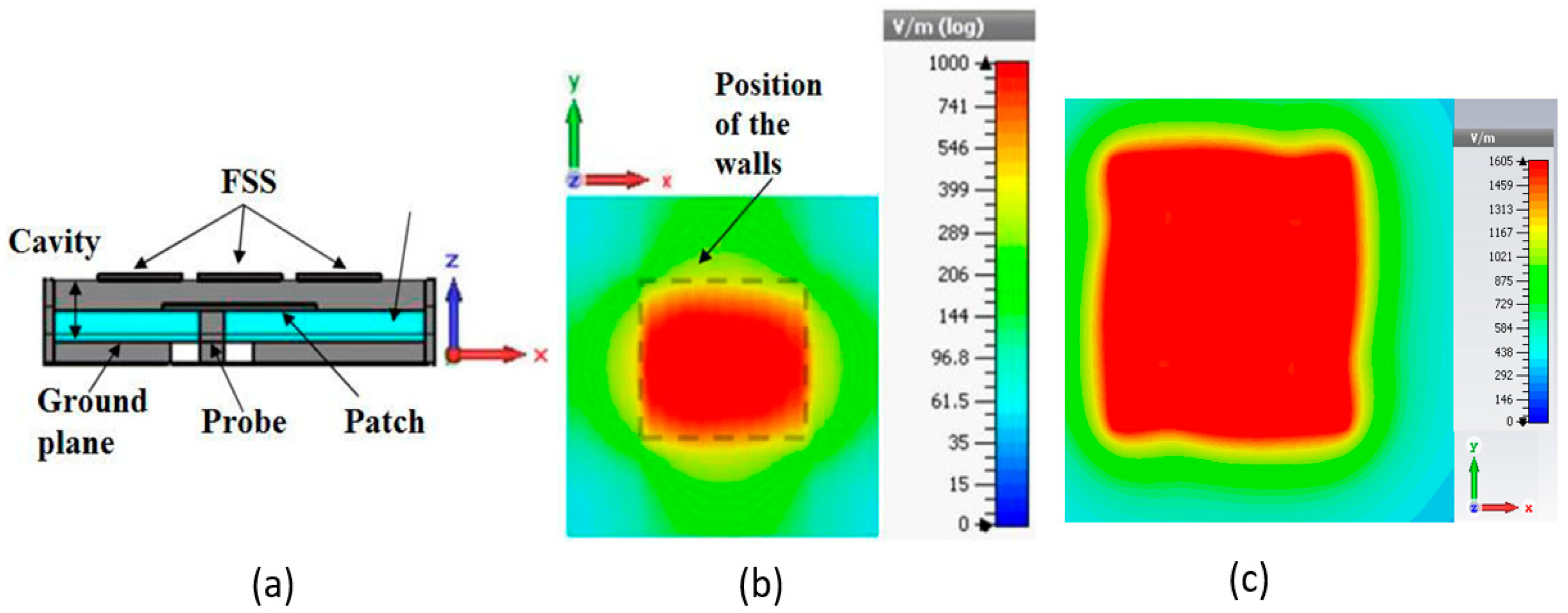
2.3. Manufacturing
2.4. Polarization
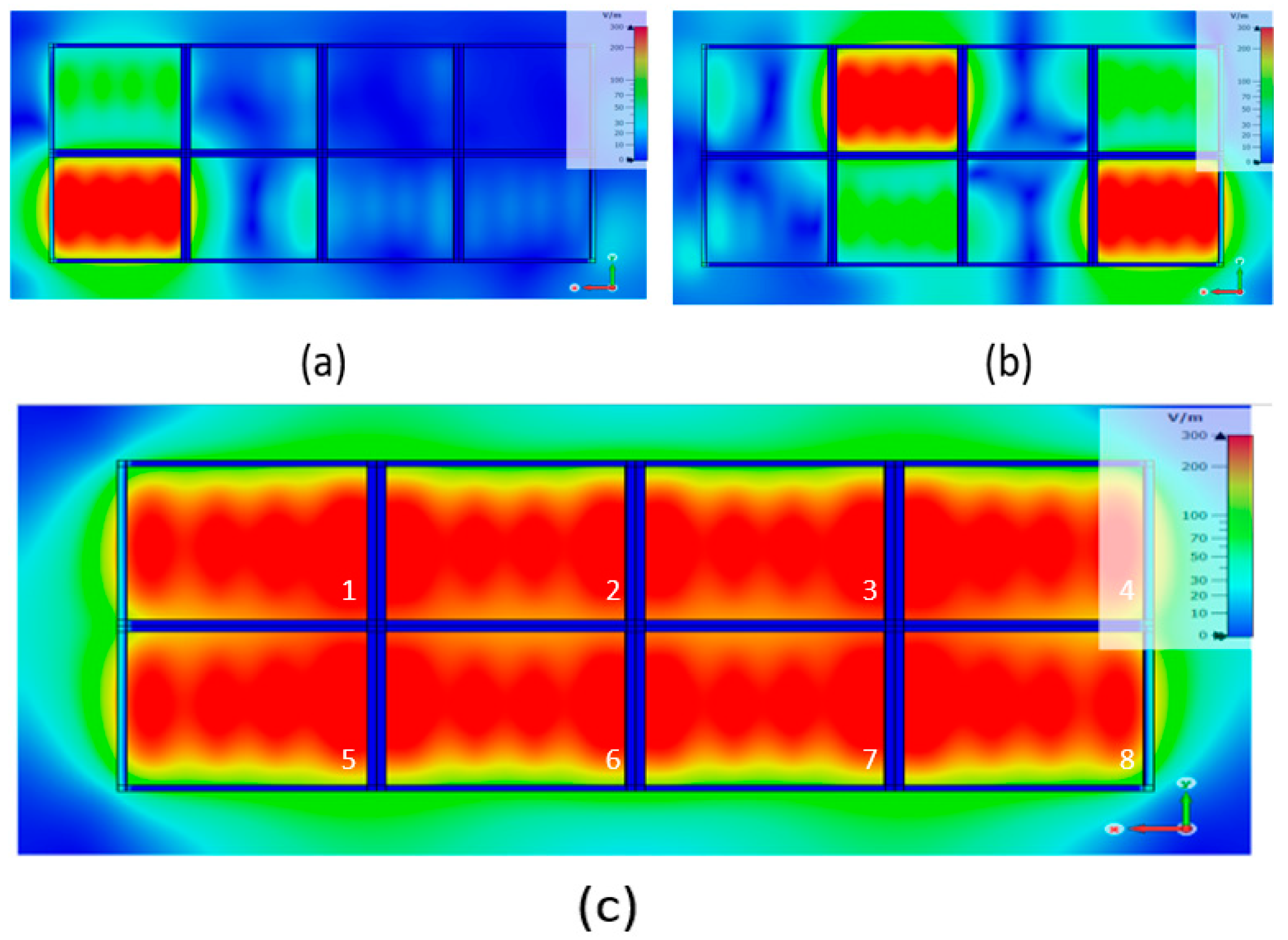
2.5. Pixel Design Theory
2.6. ARMA Construction
3. Some Applications and Comparisons with Phased Arrays
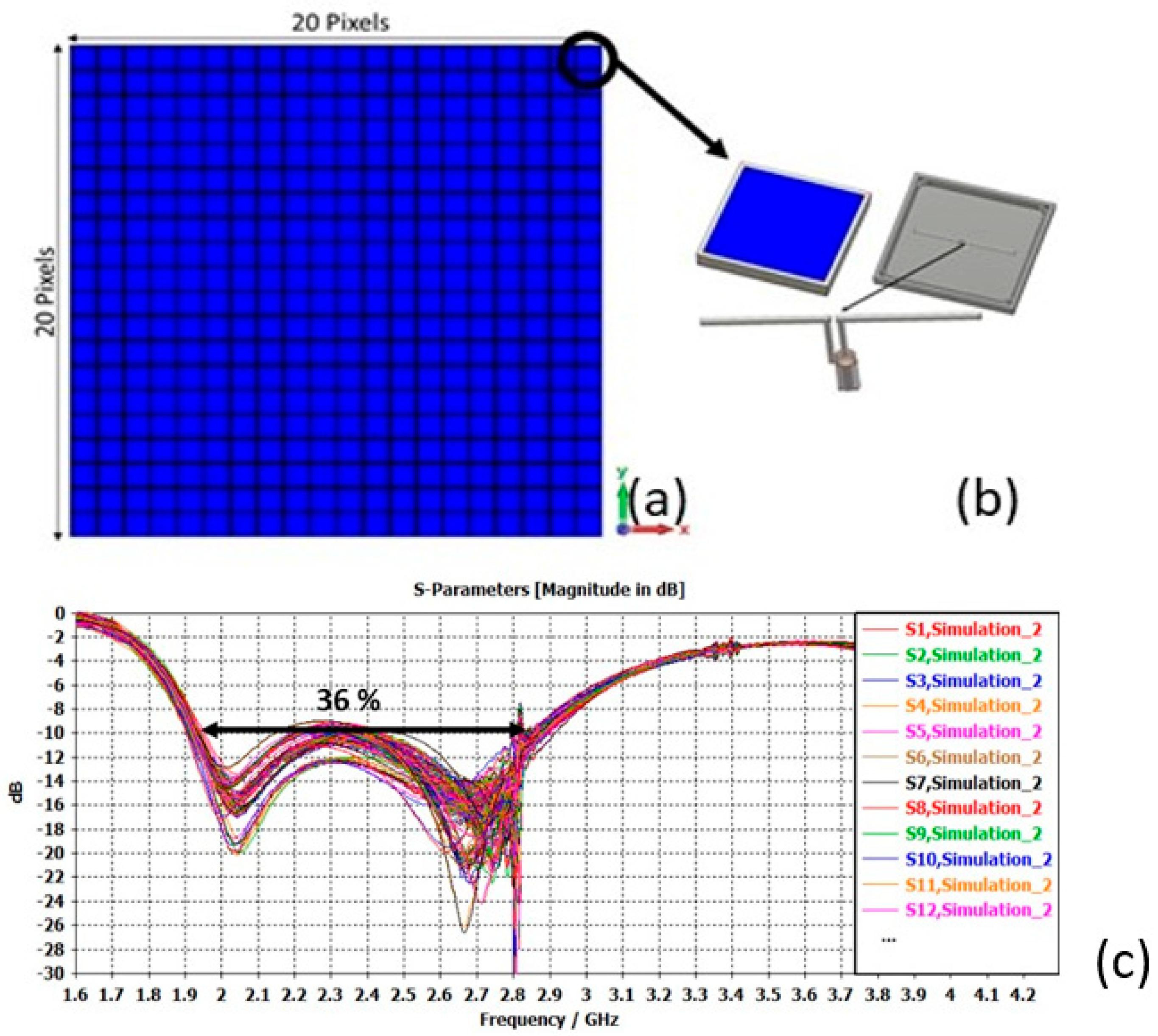
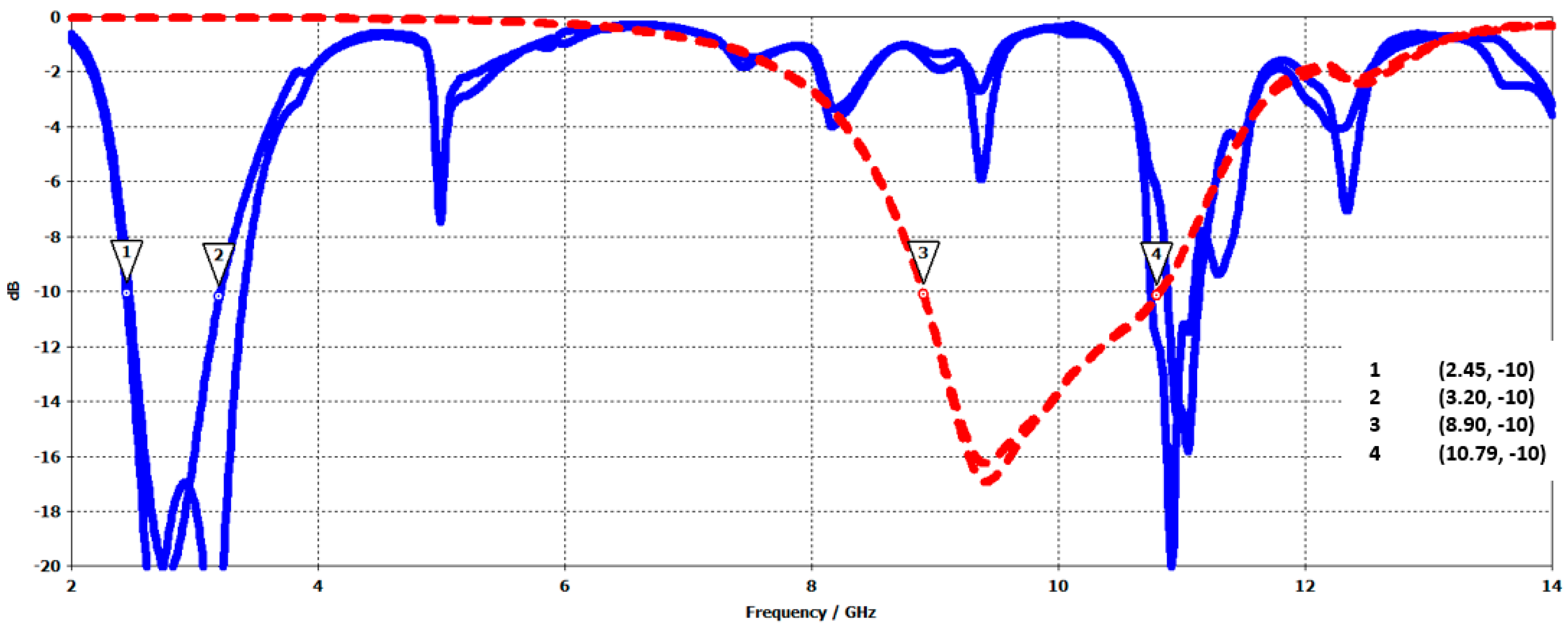
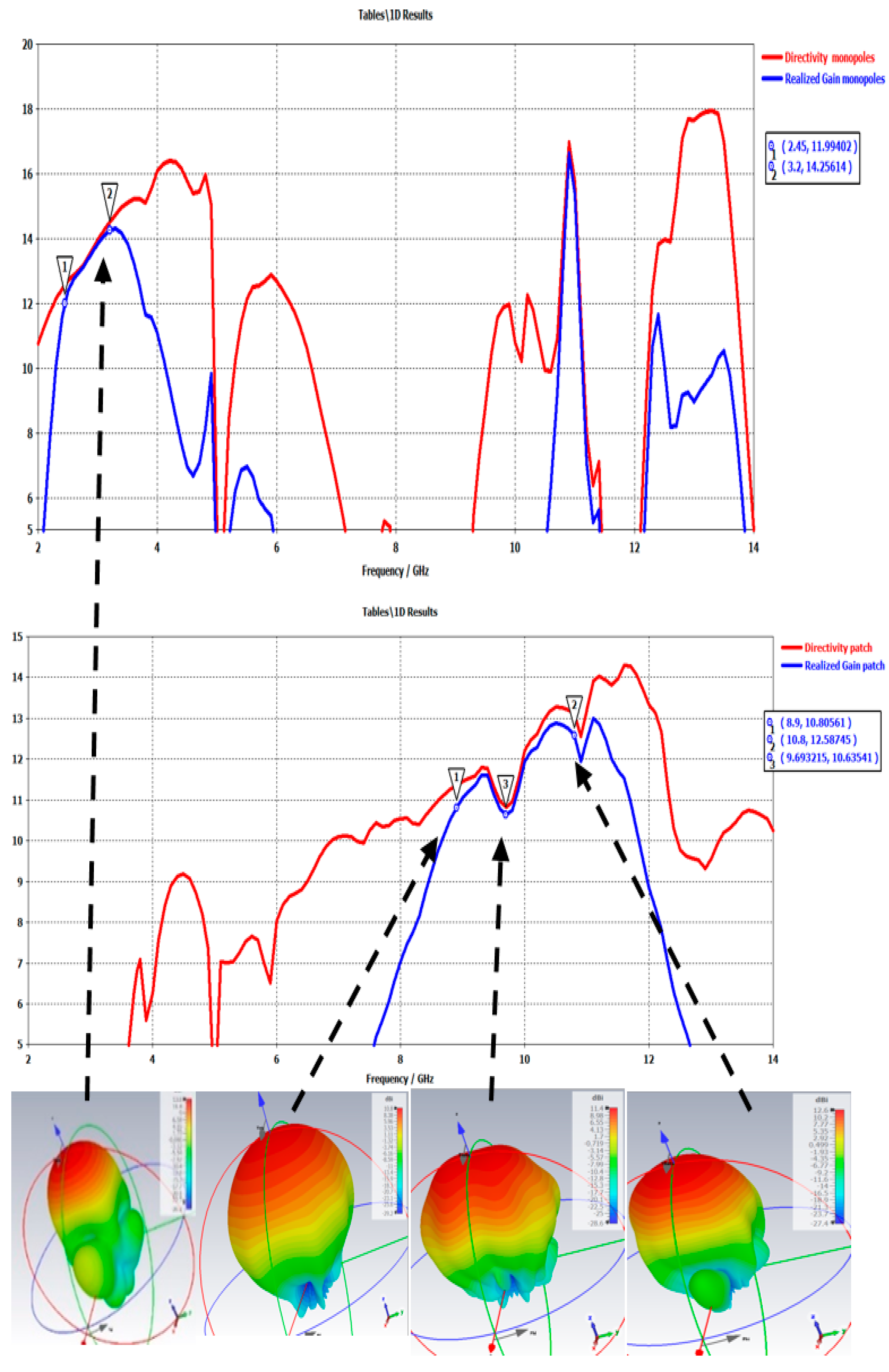
3.1. Large Bandwidth
3.1.1. Principle
3.1.2. Hole Generation in the Large Pixel Band
3.2. Beam Forming
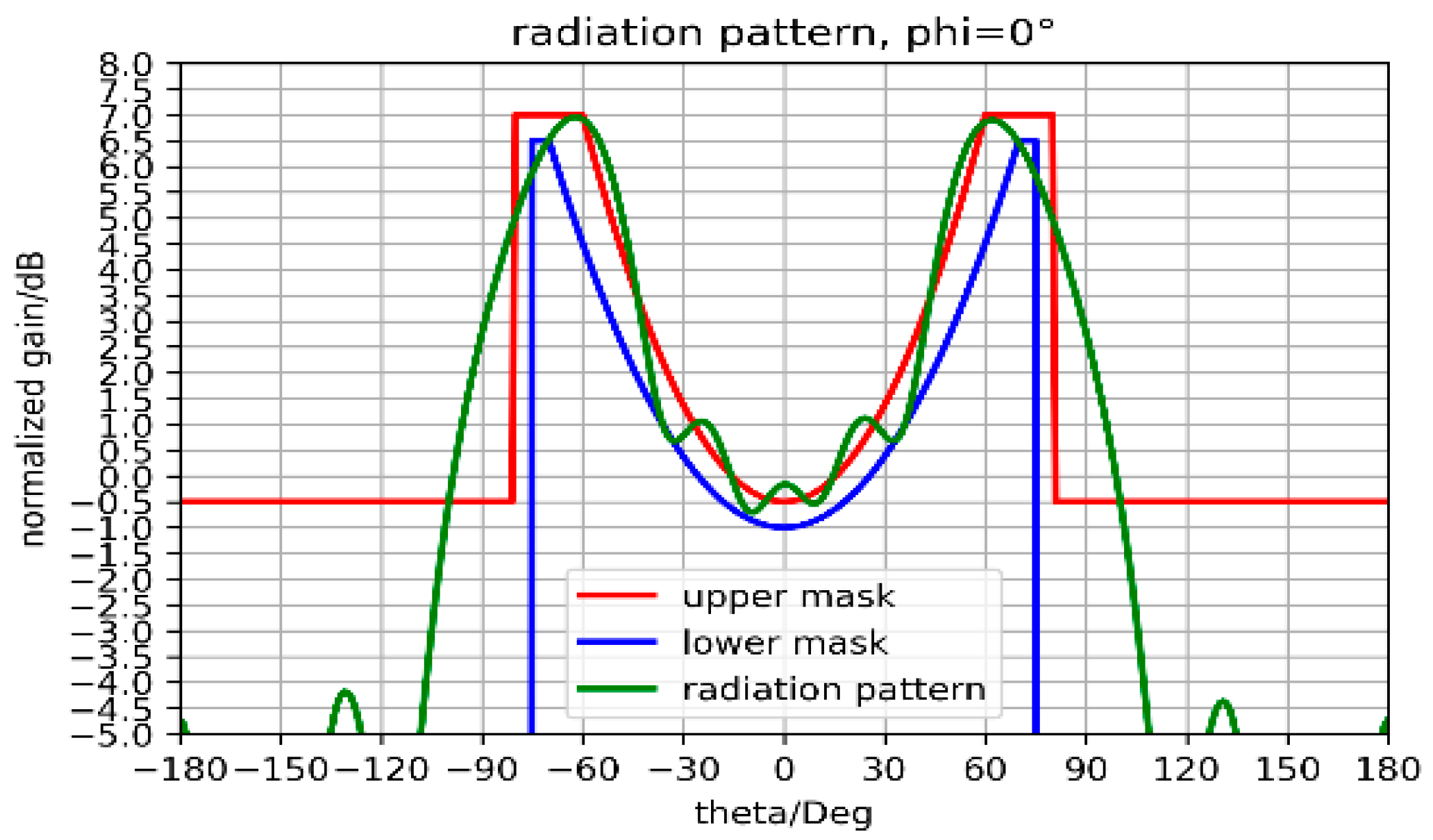
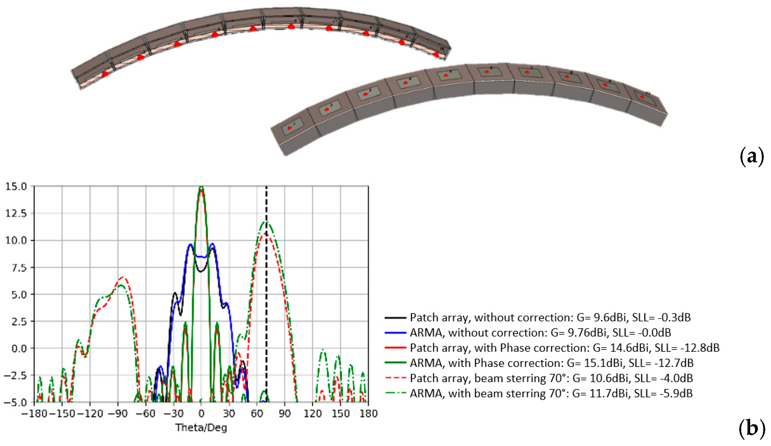
3.3. Beam Steering
- First, in the axial direction, the surface field amplitude of Es on ARMA is more uniform than this one on the array, but this difference has very little influence on the gain evolution as a function of θ.
- Second, in the 70° direction, the results are very different: the maximum gain with ARMA roughly follows the 1 + cos(θ)/2 law of Equation (1), while the maximum gain with AESA drops by around −4 dB.
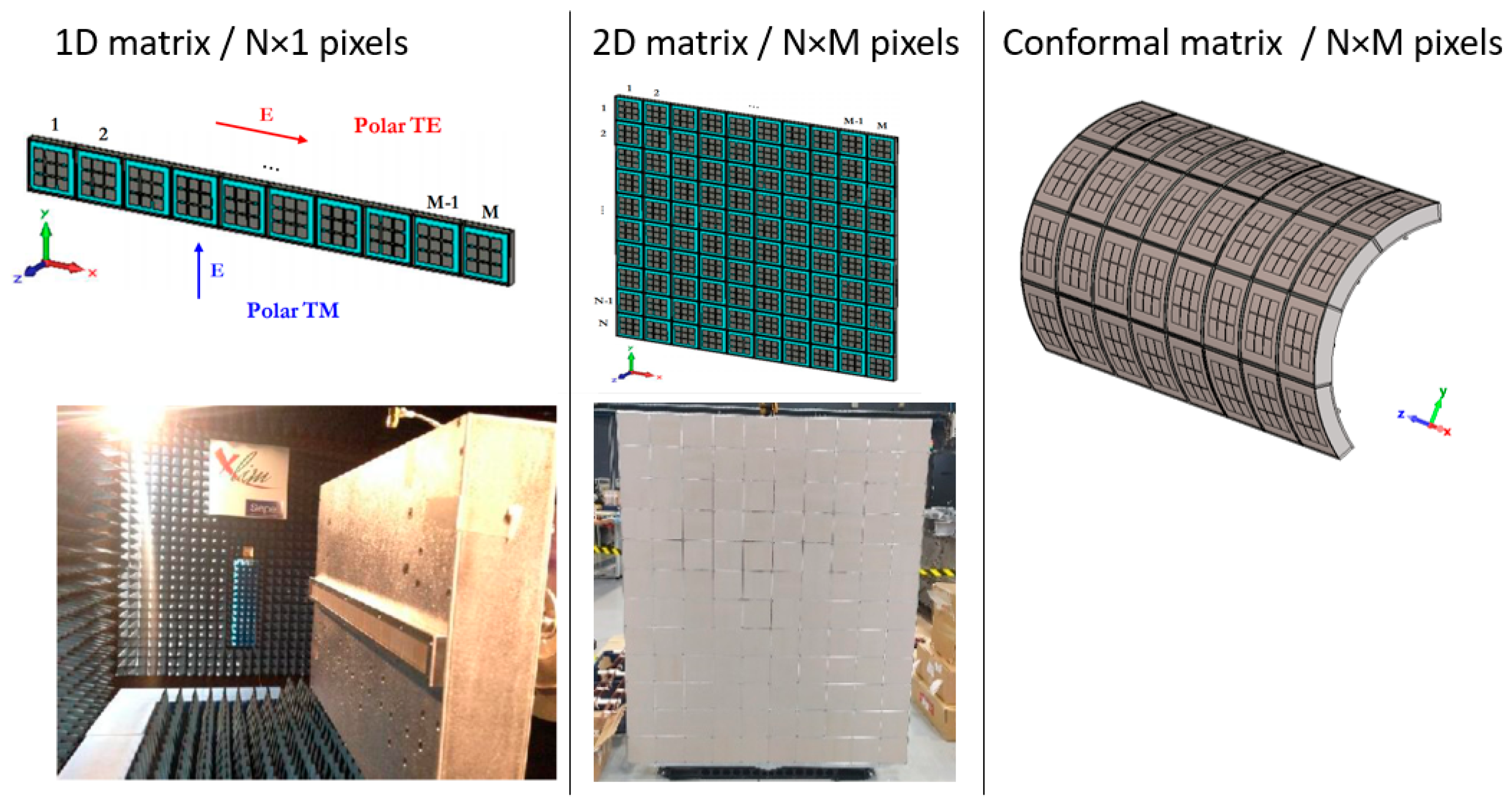
3.4. Conformal Antenna
3.5. Multifunctionality
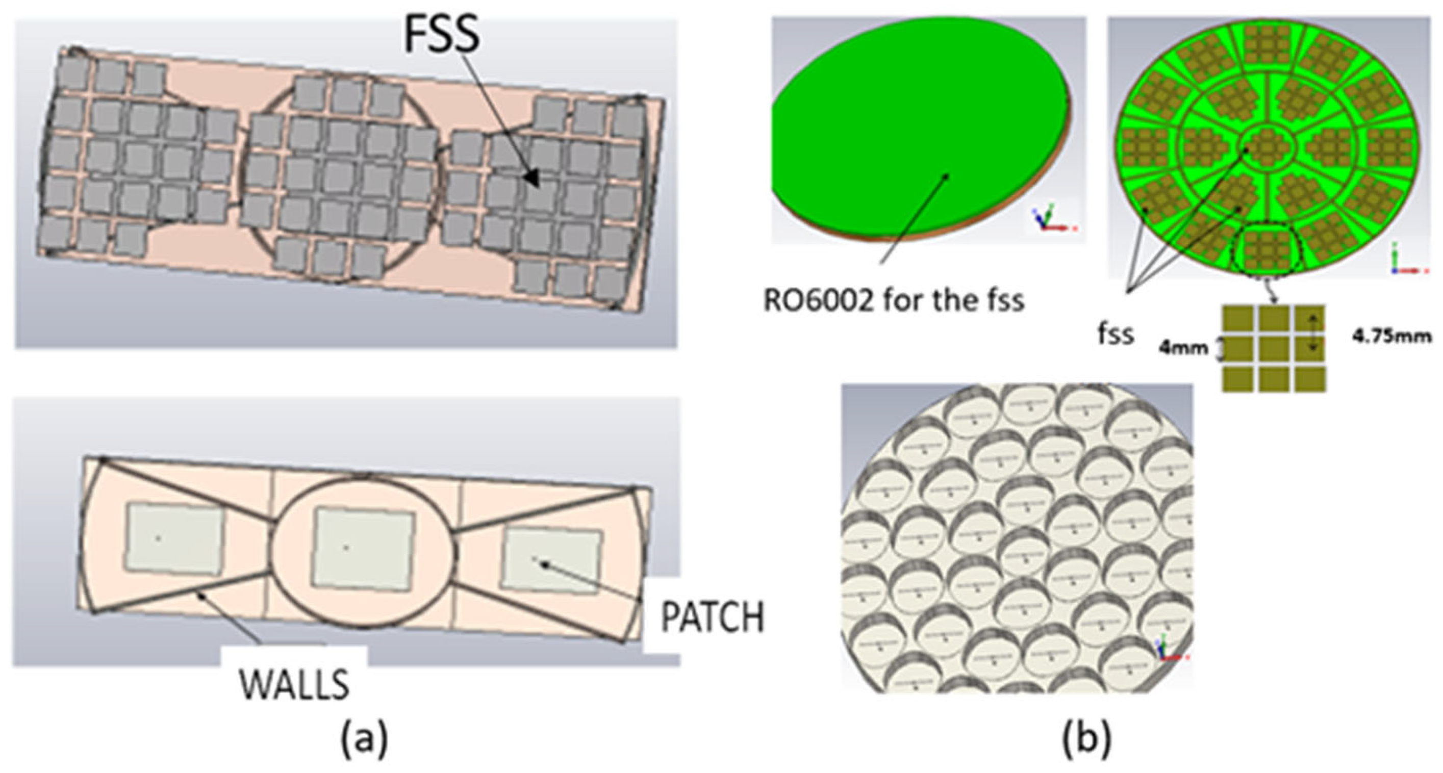
3.5.1. Band Sharing
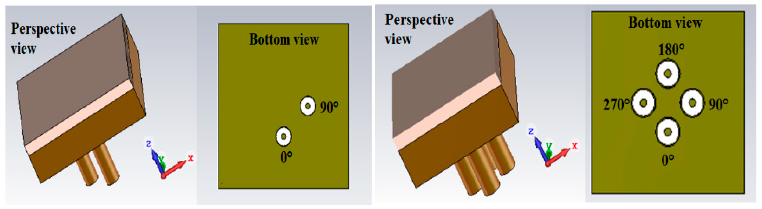
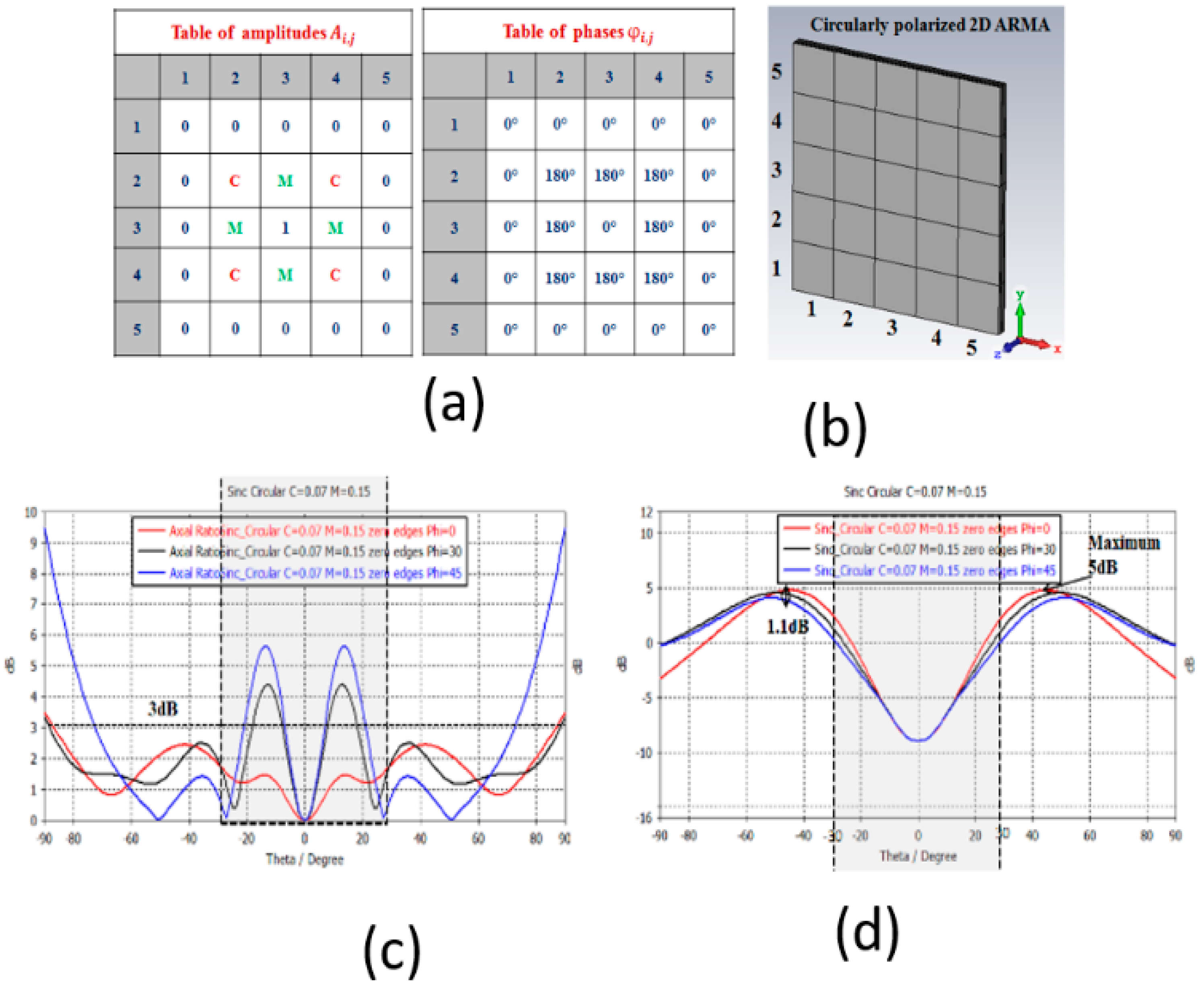
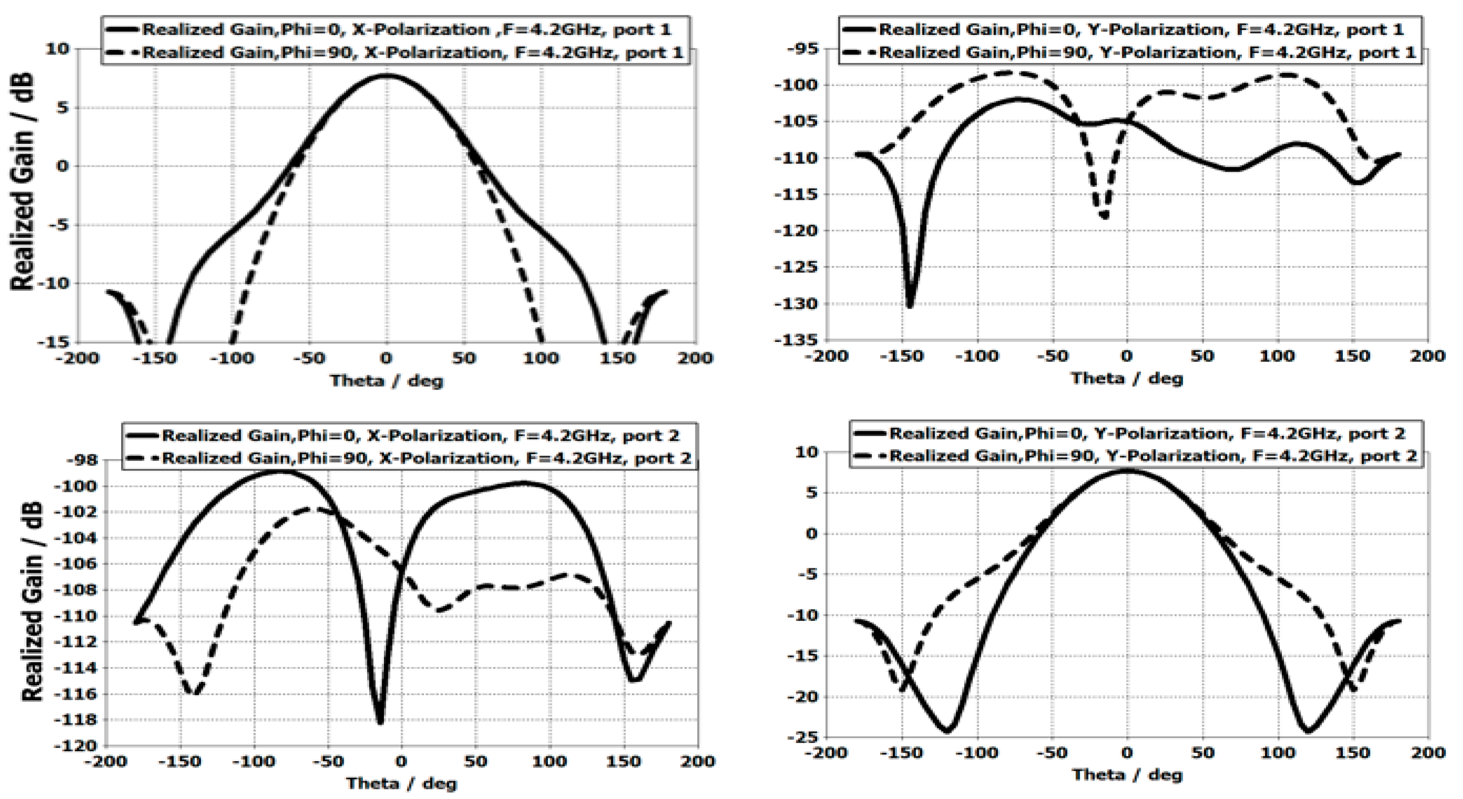
3.5.2. Generation of Orthogonal Polarization (Dual Polarization)
3.5.3. Shared Aperture Antennas
4. Conclusions
Author Contributions
Funding
Conflicts of Interest
Abbreviations
| AESA | agile electronically scanned array |
| ARMA | agile radiating matrix antenna |
| EBG | electromagnetic band gap |
| FSS | frequency selective surface |
| PRS | partially reflecting surface |
References
- Hong, W.; Jiang, Z.H.; Yu, C.; Zhou, J.; Chen, P.; Yu, Z.; Zhang, H.; Yang, B.; Pang, X.; Jiang, M.; et al. Multibeam Antenna Technologies for 5G Wireless Communications. IEEE Trans. Antennas Propag. 2017, 65, 6231–6249. [Google Scholar] [CrossRef]
- Federico, G.; Caratelli, D.; Theis, G.; Smolders, A.B. A Review of Antenna Array Technologies for Point-to-Point and Point-to-Multipoint Wireless Communications at Millimeter-Wave Frequencies. Int. J. Antennas Propag. 2021, 2021, 5559765. [Google Scholar] [CrossRef]
- Goudarzi, A.; Honari, M.M.; Mirzavand, R. Resonant Cavity Antennas for 5G Communication Systems: A Review. Electronics 2020, 9, 1080. [Google Scholar] [CrossRef]
- Mejillones, S.C.; Oldoni, M.; Moscato, S.; Fonte, A.; D’Amico, M. Power Consumption and Radiation Trade-offs in Phased Arrays for 5G Wireless Transport. In Proceedings of the 2020 43rd International Conference on Telecommunications and Signal Processing (TSP), Milan, Italy, 7–9 July 2020; pp. 112–116. [Google Scholar]
- Jecko, B. The ARMA Concept: Comparison of AESA and ARMA technologies for agile antenna design. FERMAT J. 2017, 20, 2. [Google Scholar]
- Roddier, F. Distributions et Transformation de Fourier, à L’usage des Physiciens et des Ingénieurs; Ediscience: Paris, France, 1971. [Google Scholar]
- Darricau, J. Physique et Théorie du Radar. 2015. Available online: https://radars-darricau.fr (accessed on 23 February 2024).
- Menudier, M.; Monediere, T.; Jecko, B. EBG resonator antennas: State of the art and prospects. In Proceedings of the 2007 6th International Conference on Antenna Theory and Techniques, Sevastopol, Ukraine, 17–21 September 2007; IEEE: Sevastopol, Ukraine, 2007; pp. 37–43. [Google Scholar]
- Goudarzi, A.; Movahhedi, M.; Honari, M.M.; Saghlatoon, H.; Mirzavand, R.; Mousavi, P. Wideband High-Gain Circularly Polarized Resonant Cavity Antenna with a Thin Complementary Partially Reflective Surface. IEEE Trans. Antennas Propag. 2021, 69, 532–537. [Google Scholar] [CrossRef]
- Ge, Y.; Esselle, K.P.; Bird, T.S. The Use of Simple Thin Partially Reflective Surfaces With Positive Reflection Phase Gradients to Design Wideband, Low-Profile EBG Resonator Antennas. IEEE Trans. Antennas Propag. 2012, 60, 743–750. [Google Scholar] [CrossRef]
- Hussain, N.; Jeong, M.-J.; Park, J.; Kim, N. A Broadband Circularly Polarized Fabry-Perot Resonant Antenna Using A Single-Layered PRS for 5G MIMO Applications. IEEE Access 2019, 7, 42897–42907. [Google Scholar] [CrossRef]
- Leger, L.; Monediere, T.; Jecko, B. Enhancement of gain and radiation bandwidth for a planar 1-D EBG antenna. IEEE Microw. Wirel. Compon. Lett. 2005, 15, 573–575. [Google Scholar] [CrossRef]
- Siblini, A.; Jecko, B.; Arnaud, E. Multimode reconfigurable nano-satellite antenna for PDTM application. In Proceedings of the 2017 11th European Conference on Antennas and Propagation (EUCAP), Paris, France, 19–24 March 2017; pp. 542–545. [Google Scholar]
- C Band (IEEE). Wikipedia. 29 January 2024. Available online: https://en.wikipedia.org/w/index.php?title=C_band_(IEEE)&oldid=1200625826 (accessed on 23 February 2024).
- Axness, T.A.; Coffman, R.V.; Kopp, B.A.; O’Haver, K.W. Shared Aperture Technology Development. Johns Hopkins APL Tech. Dig. 1996, 17, 285–294. [Google Scholar]
- Pozar, D.M.; Targonski, S.D. A shared-aperture dual-band dual-polarized microstrip array. IEEE Trans. Antennas Propag. 2001, 49, 150–157. [Google Scholar] [CrossRef]


Disclaimer/Publisher’s Note: The statements, opinions and data contained in all publications are solely those of the individual author(s) and contributor(s) and not of MDPI and/or the editor(s). MDPI and/or the editor(s) disclaim responsibility for any injury to people or property resulting from any ideas, methods, instructions or products referred to in the content. |
© 2025 by the authors. Licensee MDPI, Basel, Switzerland. This article is an open access article distributed under the terms and conditions of the Creative Commons Attribution (CC BY) license (https://creativecommons.org/licenses/by/4.0/).
Share and Cite
Jecko, B.; Portalier, P.-E.; Majed, M. A New Prospective Solution to Meet the New Specifications Required on Agile Beam Antennas: ARMA Theory and Applications. Sensors 2025, 25, 3381. https://doi.org/10.3390/s25113381
Jecko B, Portalier P-E, Majed M. A New Prospective Solution to Meet the New Specifications Required on Agile Beam Antennas: ARMA Theory and Applications. Sensors. 2025; 25(11):3381. https://doi.org/10.3390/s25113381
Chicago/Turabian StyleJecko, Bernard, Pierre-Etienne Portalier, and Mohamad Majed. 2025. "A New Prospective Solution to Meet the New Specifications Required on Agile Beam Antennas: ARMA Theory and Applications" Sensors 25, no. 11: 3381. https://doi.org/10.3390/s25113381
APA StyleJecko, B., Portalier, P.-E., & Majed, M. (2025). A New Prospective Solution to Meet the New Specifications Required on Agile Beam Antennas: ARMA Theory and Applications. Sensors, 25(11), 3381. https://doi.org/10.3390/s25113381