
Design of AD Converters in 0.35 µm SiGe BiCMOS Technology for Ultra-Wideband M-Sequence Radar Sensors


Abstract
1. Introduction
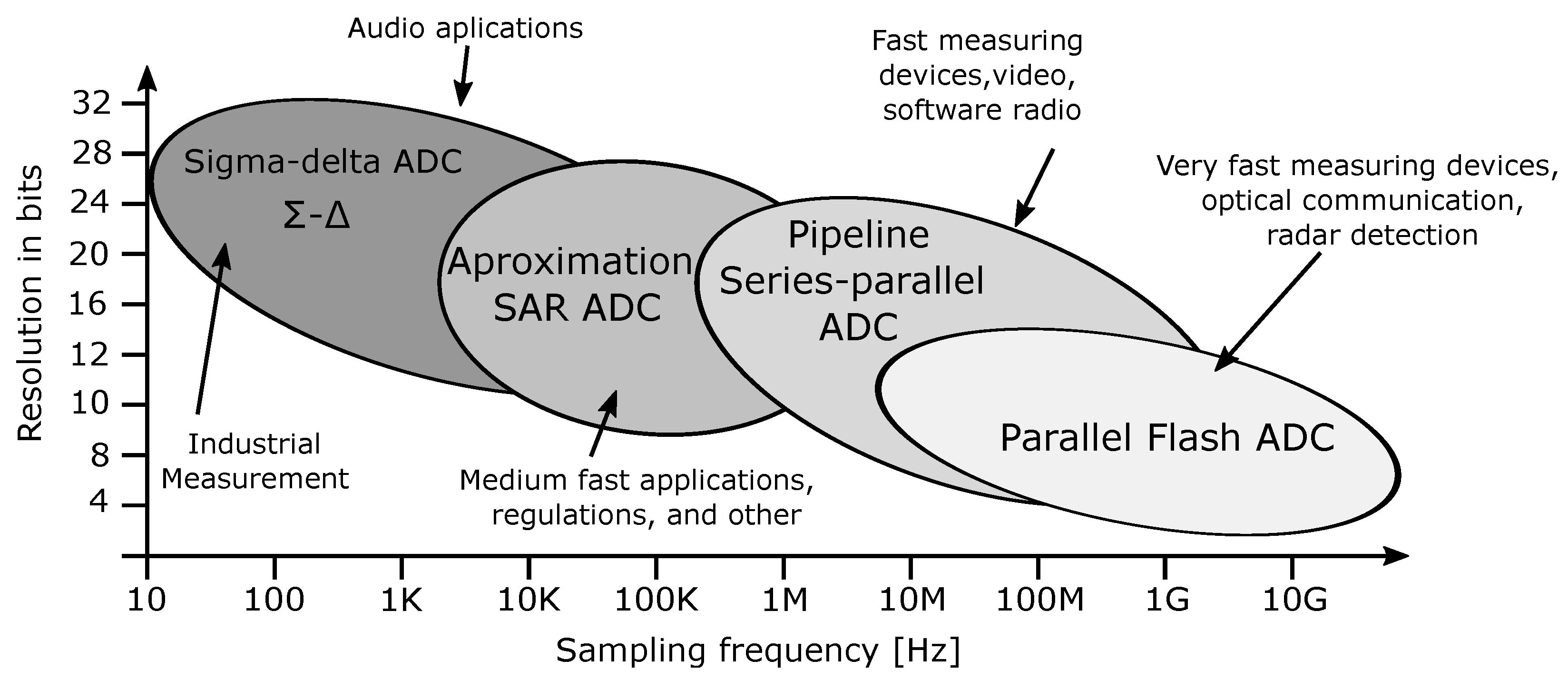
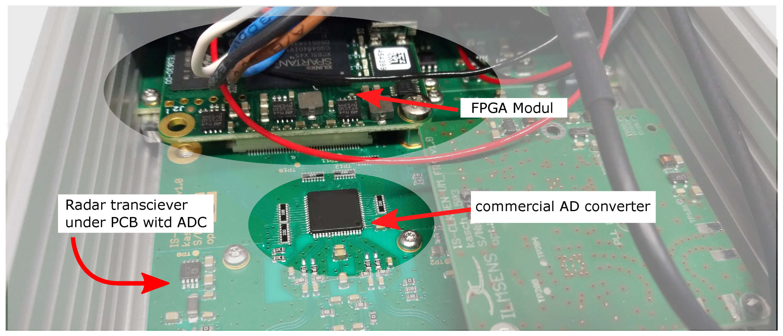
2. Current State of the AD Converter Application in the UWB M-Sequence Sensor System
- Naked die chips of commercial converters are unavailable to package with the existing UWB system, creating a SiP.
- Although it is possible to purchase the mask design of an AD converter from third parties, implemented in some technology, this can either be a new design customized specifically for the customer or a clone of an existing converter core with customized I/O circuits for the existing UWB system to create an SoC. However, the purchase of the license and design of such a converter typically costs hundreds of thousands of Euros.
- The unit cost of a custom converter in semiconductor technology.
- For the already existing analog part of the UWB system, it is possible to customize the input and output circuit levels in the case of a customer-specified converter.
- Customer-specified adjustments of converter timing.
- Easier integration of SiP and SoC.
- Custom compatible chip pinout.
- Implementation and possible design adaptation to other technologies.
- Difficulty and complexity of the customer-specified design, where both analog and digital circuits need to be considered.
- Emphasis on the design of I/O matching to the analog part of the UWB system, while possibly overlooking/neglecting the core of the converter itself and the resulting inferior AD converter parameters, such as resolution and dynamic ranges.
- Time and personnel requirements.
3. Development and Progress of the AD Converter Designs in 0.35 µm SiGe BiCMOS Technology
- Maximum number of bits per chip area, 2 × 2 mm.
- Input voltage range min. 1 Vpp.
- Lowest possible power consumption in parallel structure.
- Power supply compatible with the analog part of the UWB sensor system, −3.3 V.
- Input circuit frequency bandwidth min. 400 MHz.
- Differential inputs.
- Compatible with the analog sampling system part (without sampling circuits).
- Sampling frequency up to 100 MHz.
- Outputs compatible with negative LVCMOS standard [29].
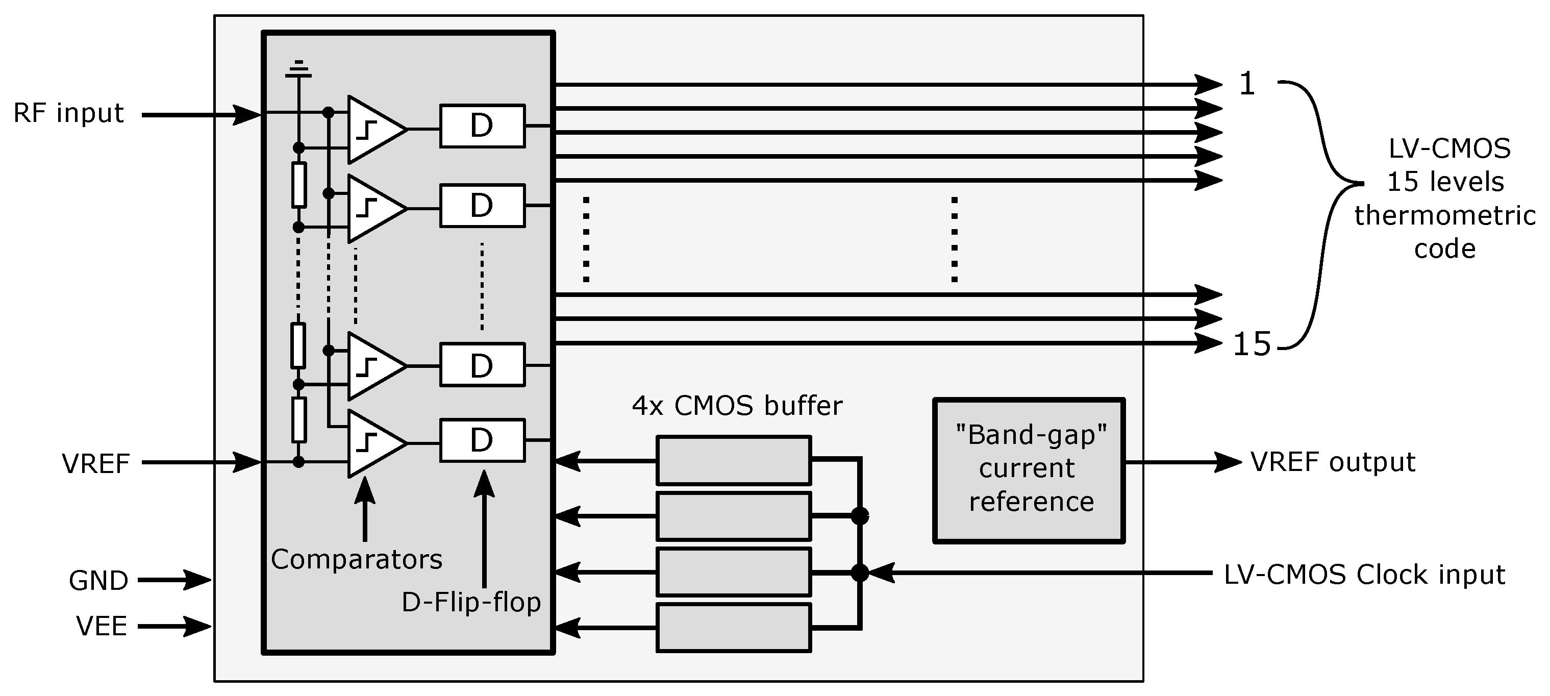
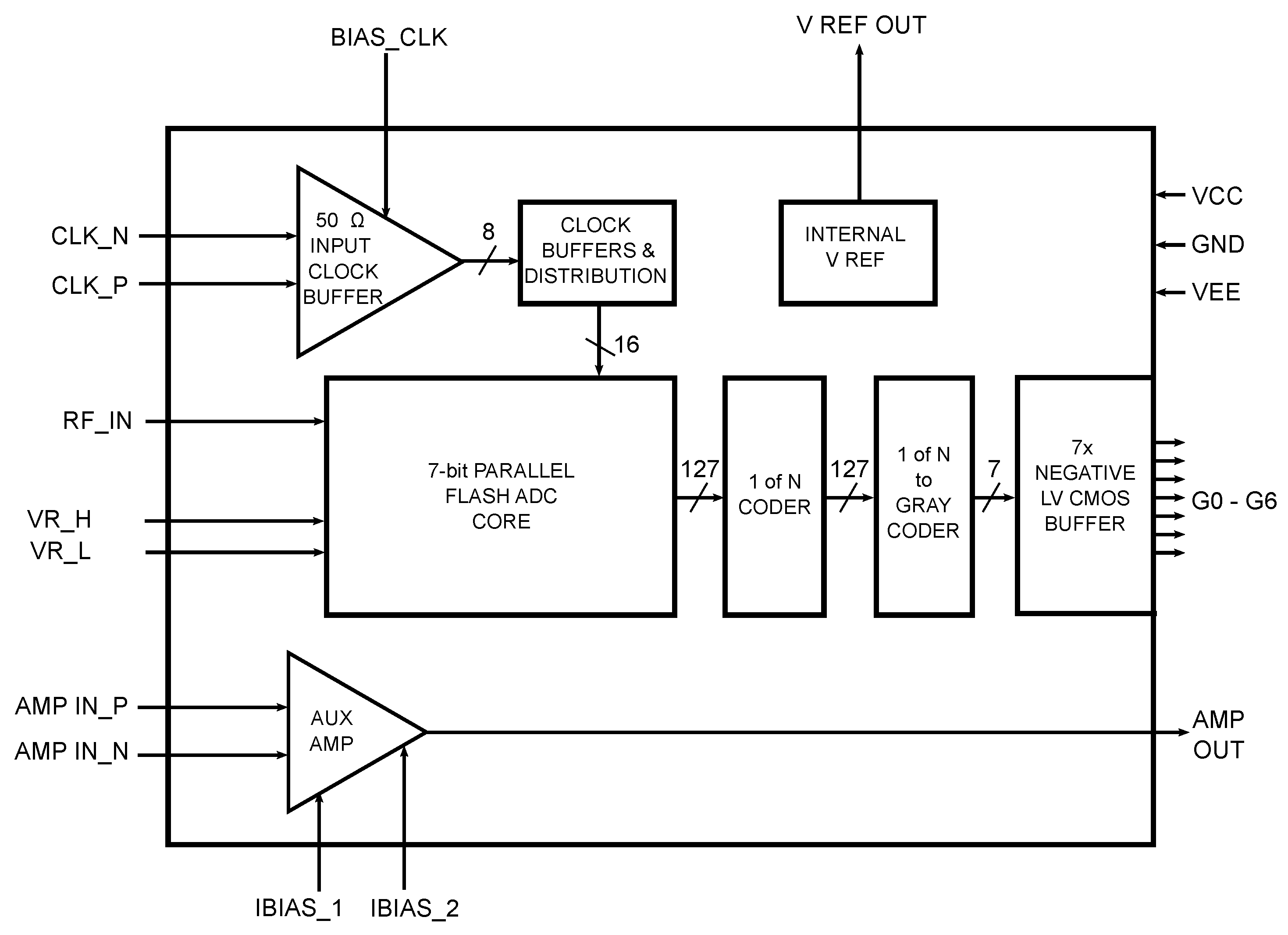
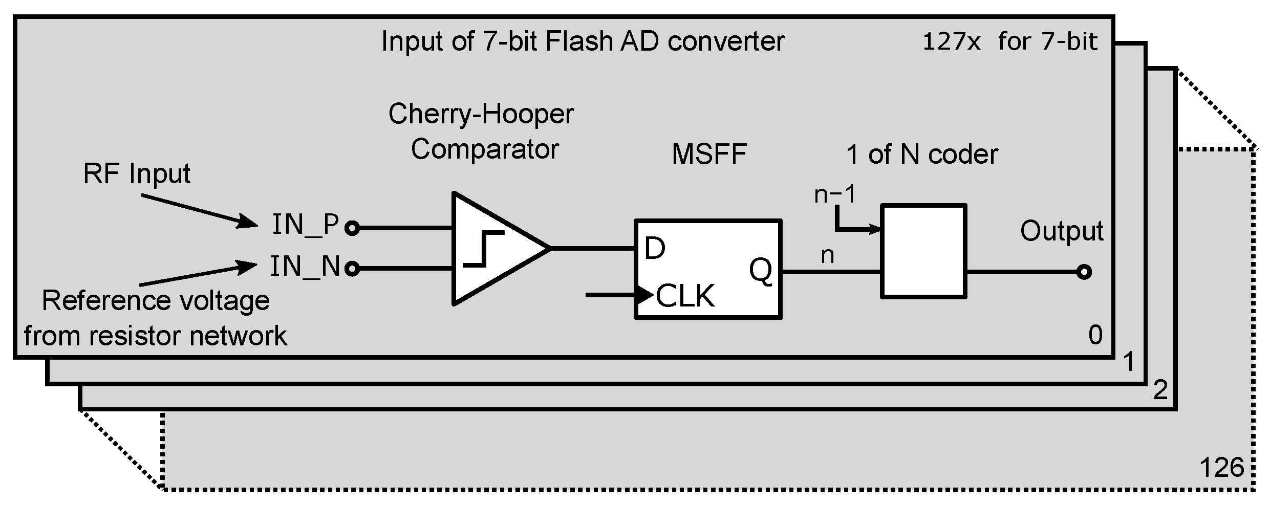
4. Design of the 7-Bit AD Converter Structure
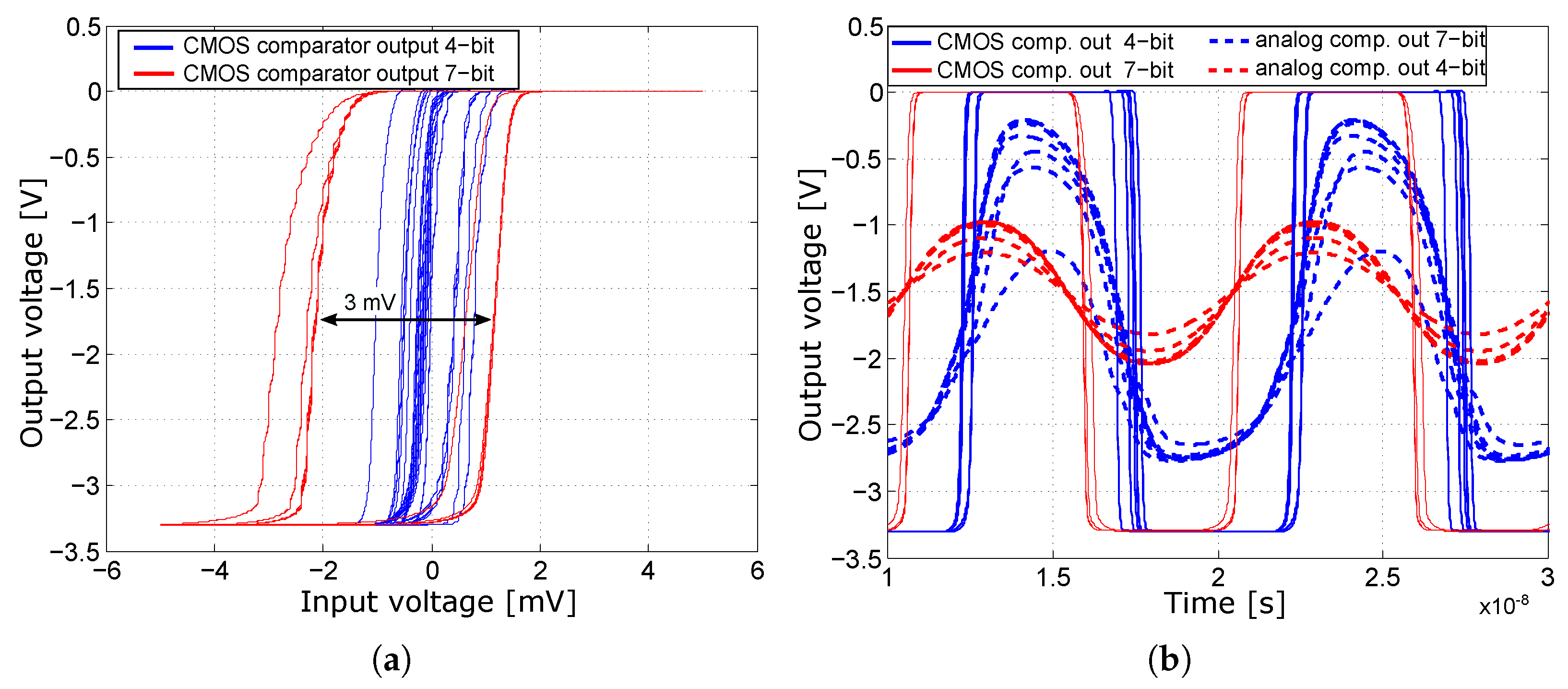
4.1. Input Circuits, Development and Enhancements
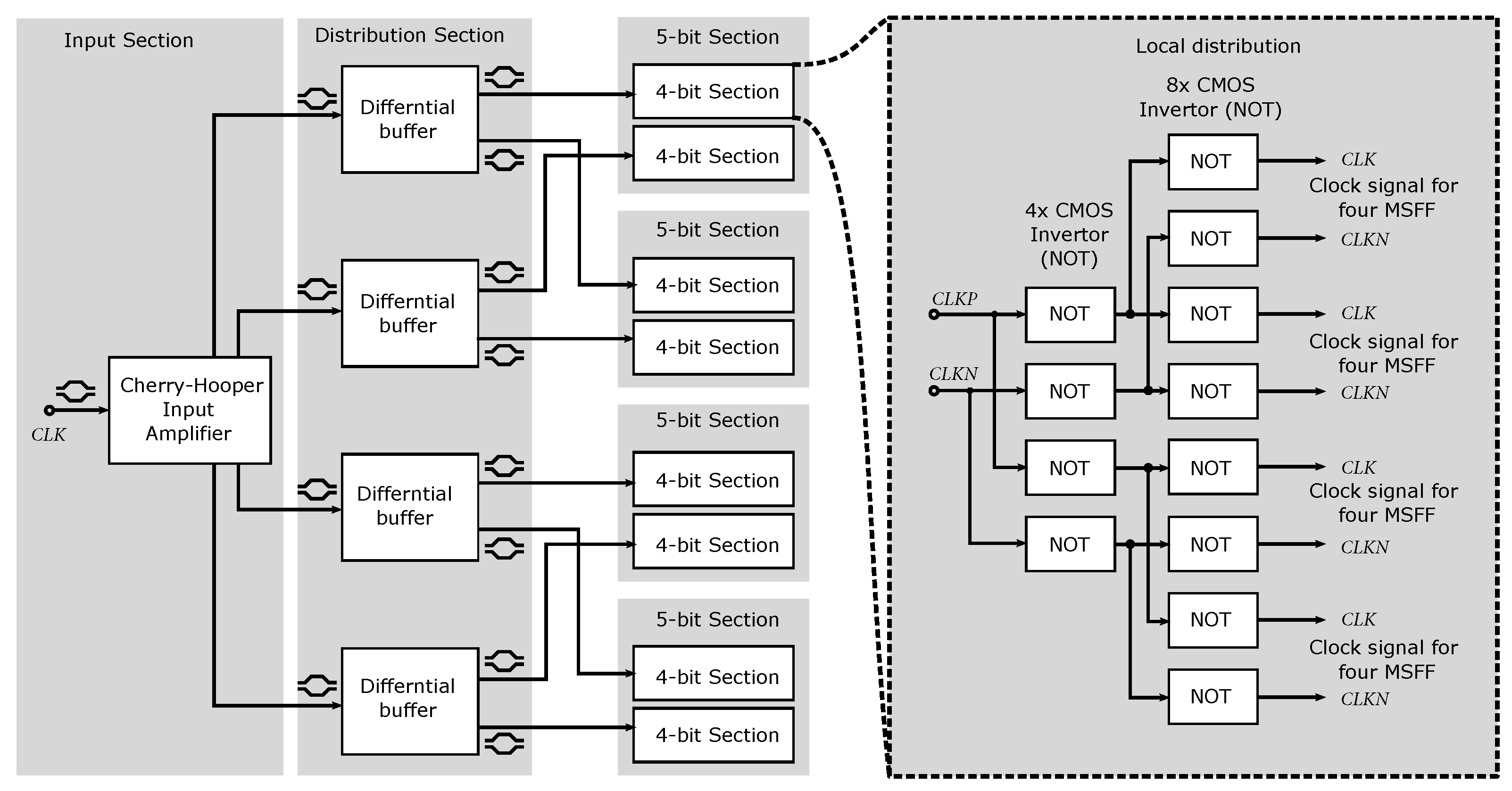
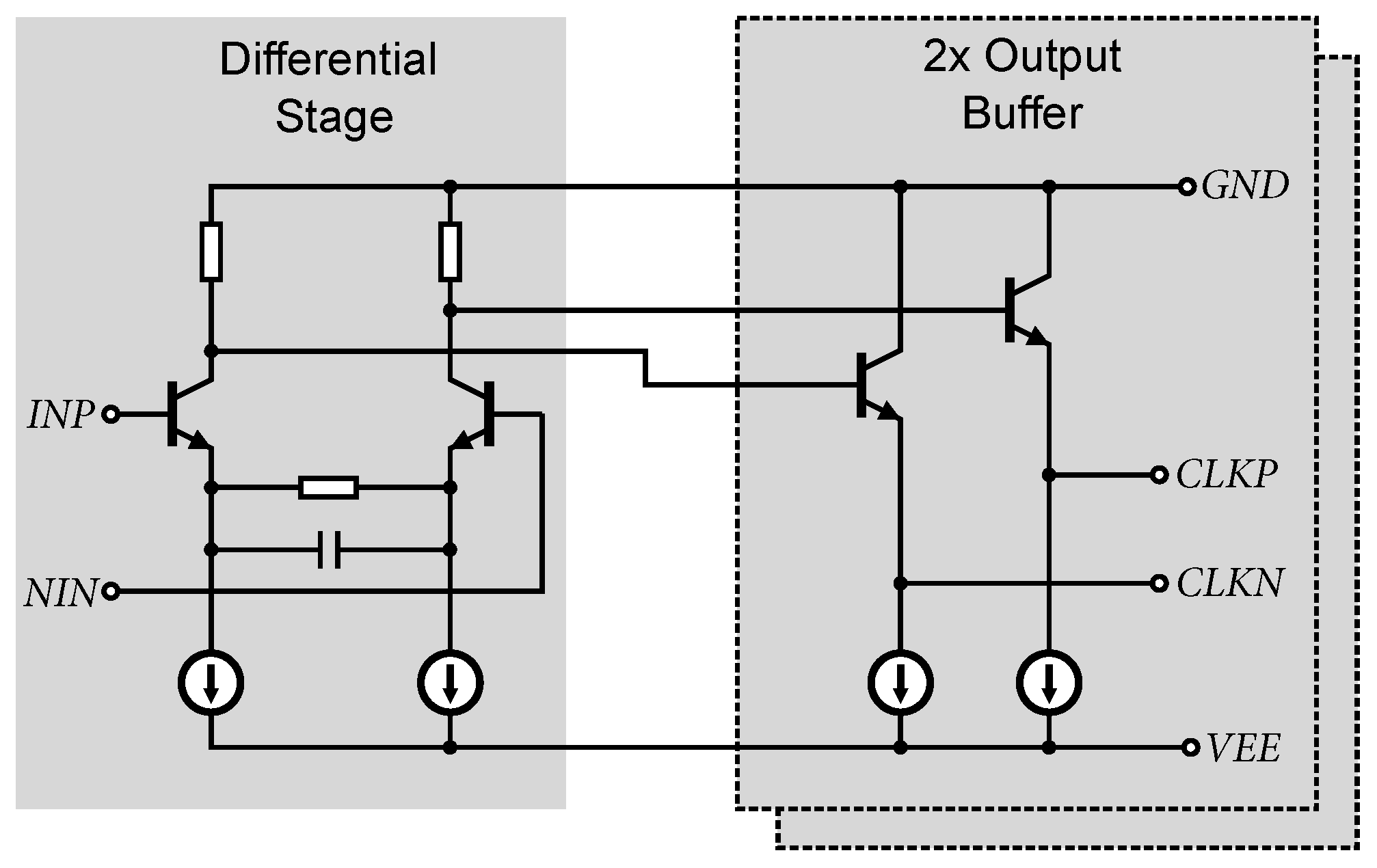
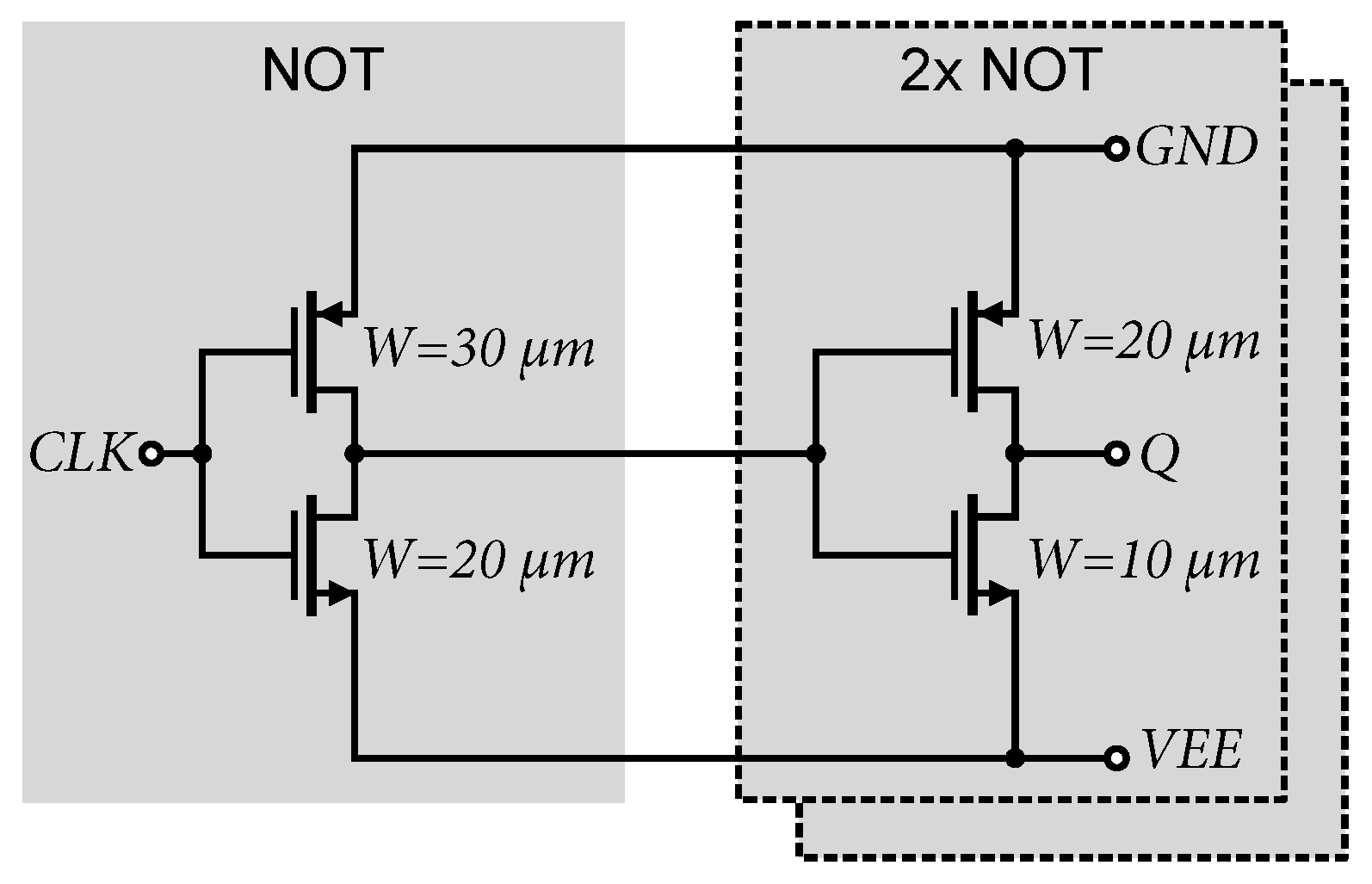
4.2. Clock Signal Distribution
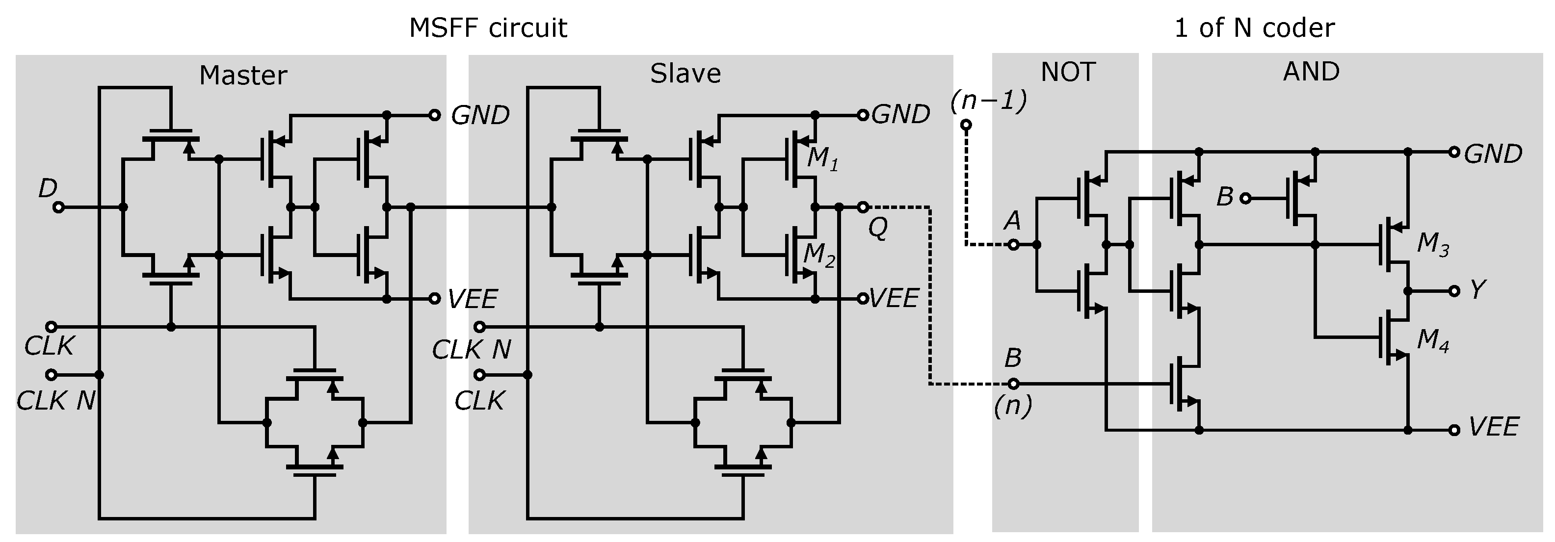
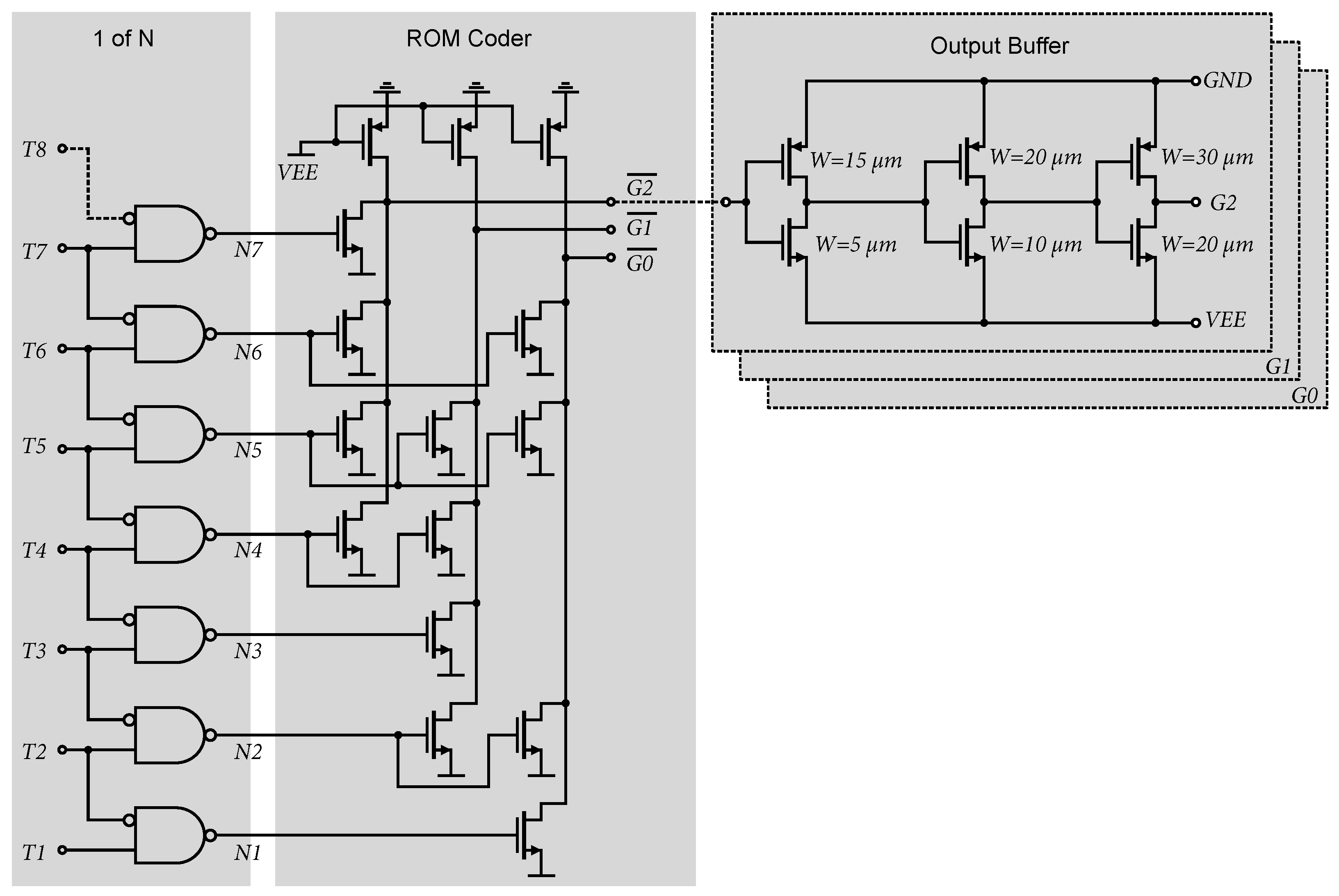
4.3. ROM Encoder and Output Circuits
4.4. Auxiliary Amplifier
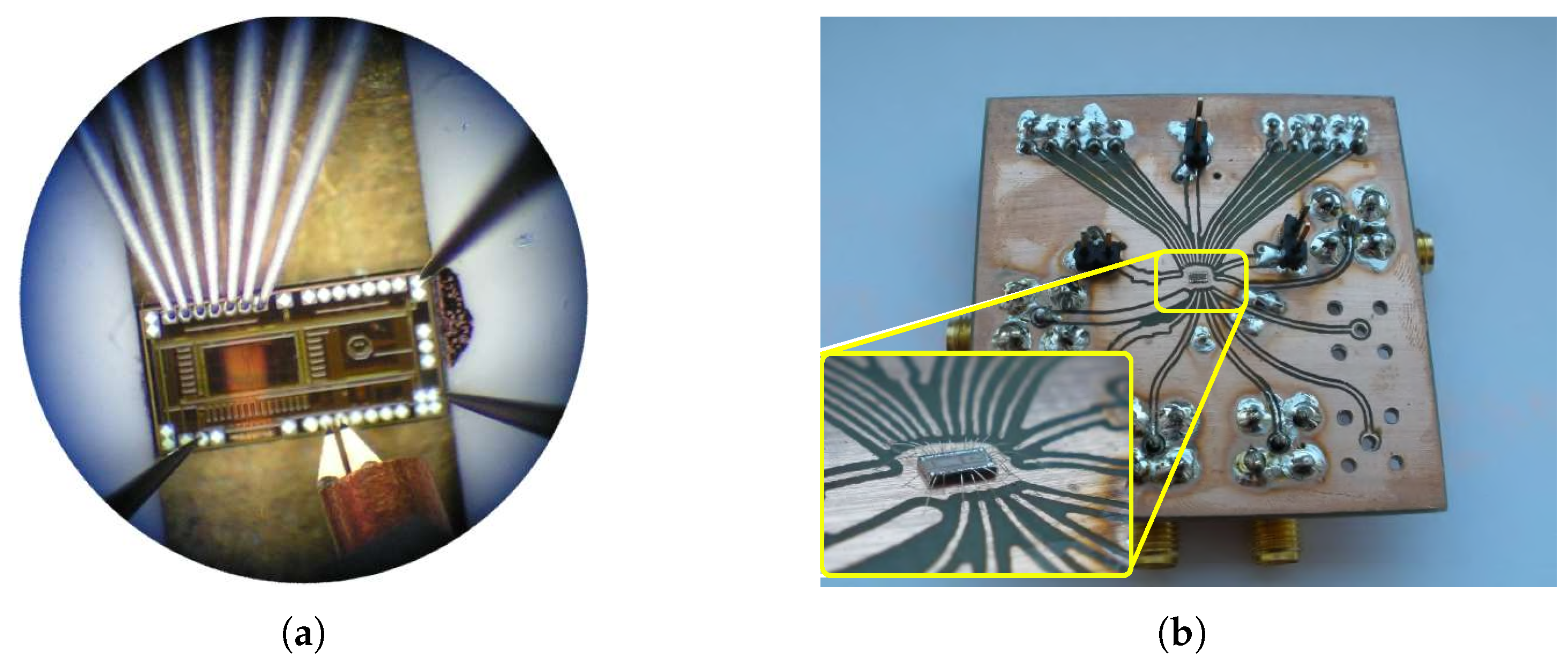
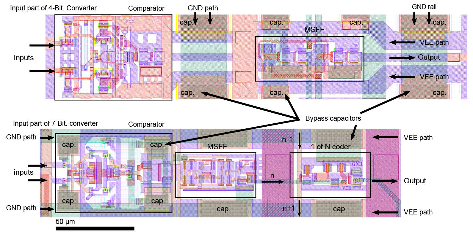
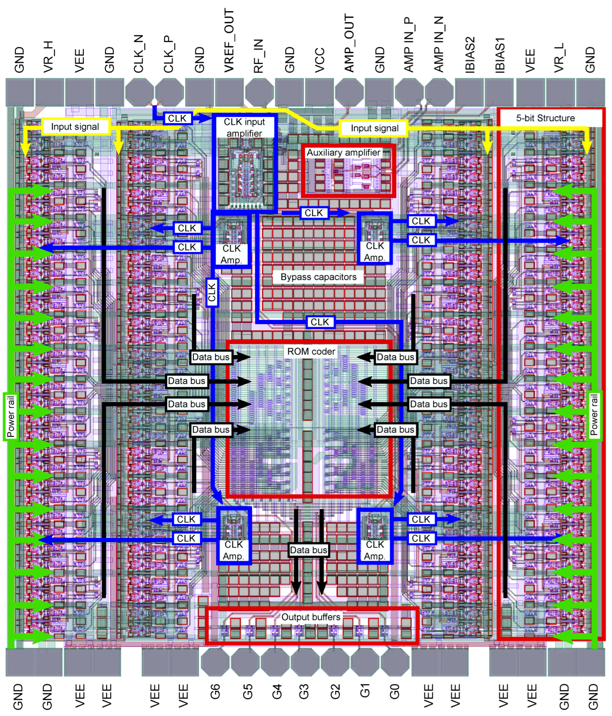
4.5. Chip Layout and Arrangement of the 7-Bit ADC
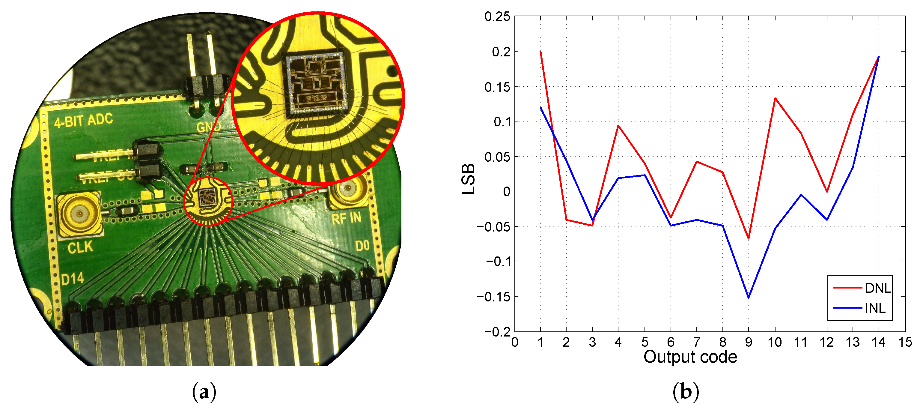
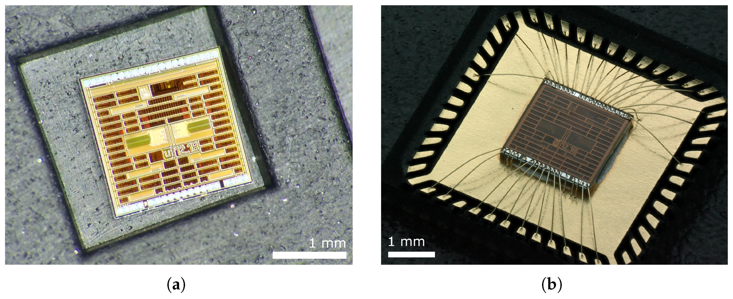
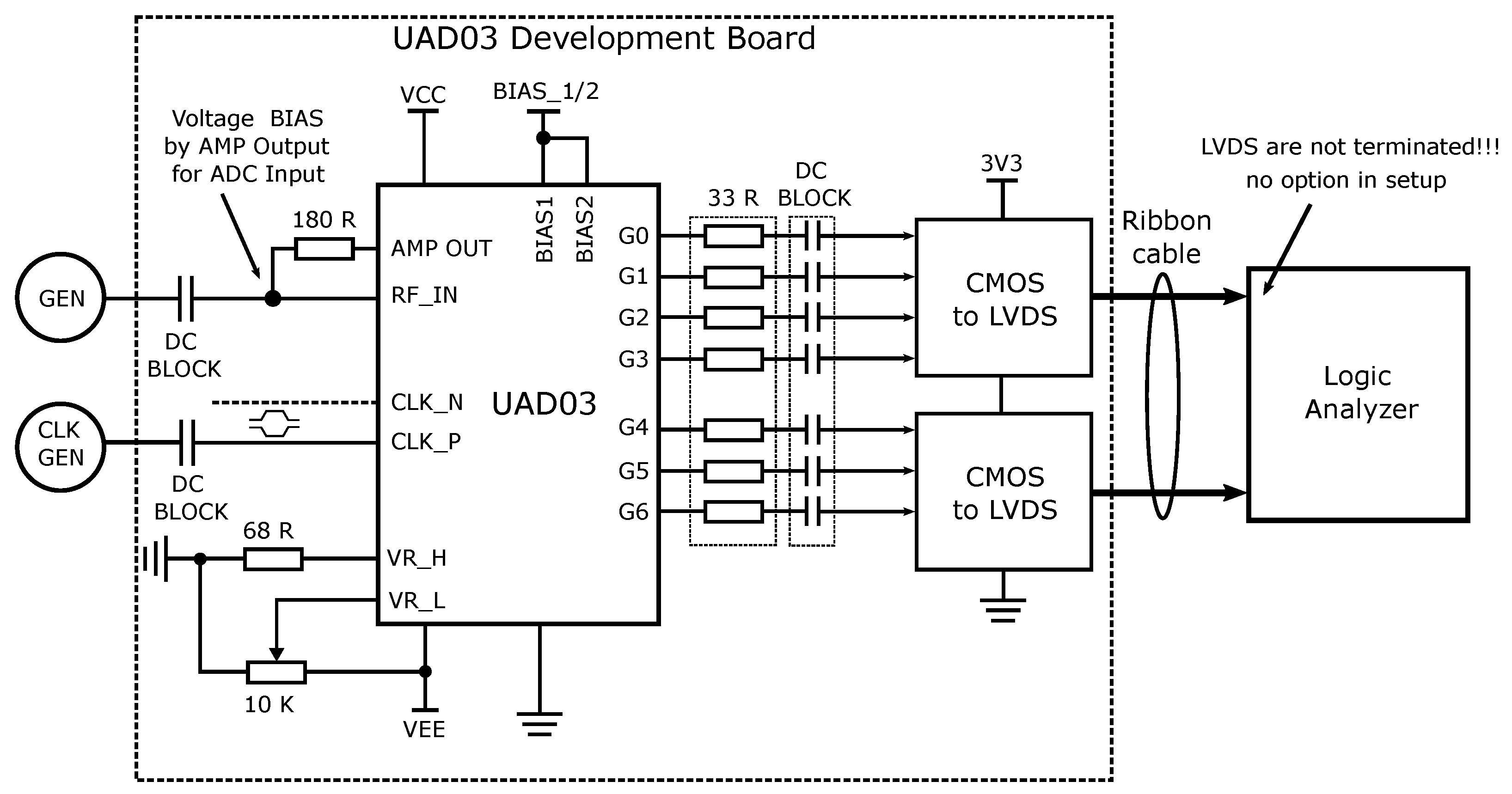
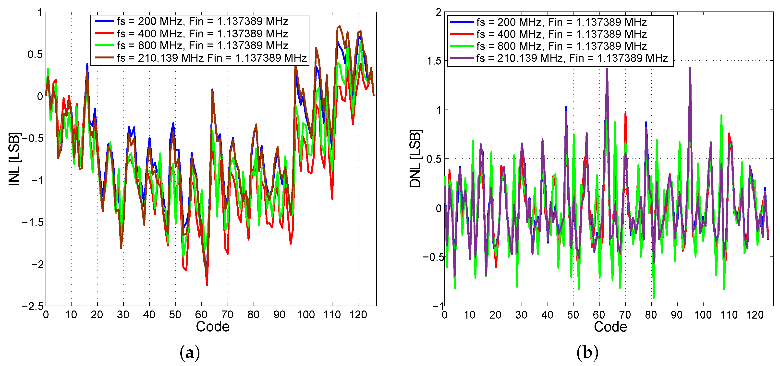
5. Development Board and Measurement
6. Conclusions
Author Contributions
Funding
Institutional Review Board Statement
Informed Consent Statement
Data Availability Statement
Conflicts of Interest
References
- Schonle, P.; Schulthess, F.; Fateh, S.; Ulrich, R.; Huang, F.; Burger, T.; Huang, Q. A DC-connectable multi-channel biomedical data acquisition ASIC with mains frequency cancellation. In Proceedings of the 2013 Proceedings of the IEEE, ESSCIRC (ESSCIRC), Bucharest, Romania, 16–20 September 2013; pp. 149–152. [Google Scholar]
- Xu, J.; Nguyen, A.T.; Wu, T.; Zhao, W.; Luu, D.K.; Yang, Z. A wide dynamic range neural data acquisition system with high-precision delta-sigma ADC and on-chip EC-PC spike processor. IEEE Trans. Biomed. Circuits Syst. 2020, 14, 425–440. [Google Scholar] [CrossRef] [PubMed]
- Kanemoto, D.; Ido, T.; Taniguchi, K. A 7.5 mW 101 dB SNR low-power high-performance audio delta-sigma modulator utilizing opamp sharing technique. In Proceedings of the 2011 International SoC Design Conference, Jeju, Republic of Korea, 17–18 November 2011; pp. 66–69. [Google Scholar] [CrossRef]
- Perez, C.; Quintero, A.; Amaral, P.; Wiesbauer, A.; Hernández, L. A 73 dB-A audio VCO-ADC based on a maximum length sequence generator in 130 nm CMOS. IEEE Trans. Circuits Syst. II Express Briefs 2021, 68, 3194–3198. [Google Scholar]
- Memon, T.R.; Halepoto, I.A.; Memon, T.D. Embedded DAQ System Design for Temperature and Humidity Measurement. Mehran Univ. Res. J. Eng. Technol. 2013, 32, 253–260. [Google Scholar]
- Dhanabalan, G.; Murugan, T. FPGA design of SAR type ADC based analog input module for industrial applications. In Proceedings of the Advances in VLSI and Embedded Systems: Select Proceedings of AVES 2019; Springer: Singapore, 2021; pp. 97–113. [Google Scholar] [CrossRef]
- Li, C.; Vankayalapati, B.; Akin, B. Latency compensation of SD-ADC for high performance motor control and diagnosis. In Proceedings of the 2021 IEEE 13th International Symposium on Diagnostics for Electrical Machines, Power Electronics and Drives (SDEMPED), Dallas, TX, USA, 22–25 August 2021; Volume 1, pp. 289–294. [Google Scholar]
- Mochizuki, K.; Uchino, M.; Morikawa, T. Frequency-stability measurement system using high-speed ADCs and digital signal processing. IEEE Trans. Instrum. Meas. 2007, 56, 1887–1893. [Google Scholar] [CrossRef]
- Wu, Y.; Li, S.; Luo, L.; Ye, F.; Ren, J. An area-power-efficient AFE with NS-SAR ADC for high-frequency ultrasound applications. In Proceedings of the 2020 IEEE Asia Pacific Conference on Circuits and Systems (APCCAS), Ha Long, Vietnam, 8–10 December 2020; pp. 7–10. [Google Scholar]
- Seo, M.W.; Chu, M.; Jung, H.Y.; Kim, S.; Song, J.; Lee, J.; Kim, S.Y.; Lee, J.; Byun, S.J.; Bae, D.; et al. A 2.6 e-rms low-random-noise, 116.2 mW low-power 2-Mp global shutter CMOS image sensor with pixel-level ADC and in-pixel memory. In Proceedings of the IEEE 2021 Symposium on VLSI Technology, Kyoto, Japan, 13–19 June 2021; pp. 1–2. [Google Scholar]
- Rapuano, S.; Daponte, P.; Balestrieri, E.; Vito, L.D.; Tilden, S.J.; Max, S.; Blair, J. ADC parameters and characteristics. IEEE Instrum. Meas. Mag. 2005, 8, 44–54. [Google Scholar] [CrossRef]
- Chen, D.; Cui, X.; Zhang, Q.; Li, D.; Cheng, W.; Fei, C.; Yang, Y. A survey on analog-to-digital converter integrated circuits for miniaturized high resolution ultrasonic imaging system. Micromachines 2022, 13, 114. [Google Scholar] [CrossRef] [PubMed]
- Karpe, A.; Prateek, M. Comparative Analysis of CMOS ADC Topologies with Different Performance Parameters. IOSR J. VLSI Signal Process. 2013, 3, 61–69. [Google Scholar] [CrossRef]
- Mayur, S.; Siddharth, R.; Nithin Kumar, Y.B.; Vasantha, M. Design of Low Power 4-Bit 400 MS/s Standard Cell Based Flash ADC. In Proceedings of the 2017 IEEE Computer Society Annual Symposium on VLSI (ISVLSI), Bochum, Germany, 3–5 July 2017; pp. 600–603. [Google Scholar]
- Zandieh, A.; Schvan, P.; Voinigescu, S.P. A 2x-Oversampling, 128-GS/s 5-bit Flash ADC for 64-GBaud Applications. In Proceedings of the 2018 IEEE BiCMOS and Compound Semiconductor Integrated Circuits and Technology Symposium (BCICTS), San Diego, CA, USA, 15–17 October 2018; pp. 52–55. [Google Scholar] [CrossRef]
- Liptaj, M.; Ziga, M.; Galajda, P. Design of the 5-bit Flash AD Converter for UWB Applications. In Proceedings of the 12th Scientific Conference of Young Researchers, Herlany, Slovakia, 15 May 2012. [Google Scholar]
- Devarajan, S.; Singer, L.; Kelly, D.; Pan, T.; Silva, J.; Brunsilius, J.; Rey-Losada, D.; Murden, F.; Speir, C.; Bray, J.; et al. A 12-b 10-GS/s Interleaved Pipeline ADC in 28-nm CMOS Technology. IEEE J. Solid-State Circuits 2017, 52, 3204–3218. [Google Scholar] [CrossRef]
- Tuite, D. Relate ADC Topologies And Performance To Applications-ENGINEERING ESSENTIALS. Electron. Des. 2012, 60, 38. [Google Scholar]
- Zheng, Y.; Zhao, Y.; Zhou, N.; Wang, H.; Jiang, D. A short review of some analog-to-digital converters resolution enhancement methods. Measurement 2021, 180, 109554. [Google Scholar] [CrossRef]
- Seong, K.; Jung, D.K.; Yoon, D.H.; Han, J.S.; Kim, J.E.; Kim, T.T.H.; Lee, W.; Baek, K.H. Time-interleaved SAR ADC with background timing-skew calibration for UWB wireless communication in IoT systems. Sensors 2020, 20, 2430. [Google Scholar] [CrossRef] [PubMed]
- Tilden, S.J.; Linnenbrink, T.E.; Green, P.J. Overview of IEEE-STD-1241 “standard for terminology and test methods for analog-to-digital converters”. In Proceedings of the IMTC/99. Proceedings of the 16th IEEE Instrumentation and Measurement Technology Conference (Cat. No. 99CH36309), Venice, Italy, 24–26 May 1999; Volume 3, pp. 1498–1503. [Google Scholar]
- Galajda, P.; Pecovsky, M.; Gazda, J.; Drutarovsky, M. Novel M-sequence UWB sensor for ground penetrating radar application. In Proceedings of the 2018 IEEE Asia-Pacific Conference on Antennas and Propagation (APCAP), Auckland, New Zealand, 5–8 August 2018; pp. 110–111. [Google Scholar]
- Pecovsky, M.; Sokol, M.; Galajda, P. 15 th Order M-sequence SoC Radar for Short-Range Sensing. In Proceedings of the IEEE 2020 21st International Radar Symposium (IRS), Warsaw, Poland, 5–8 October 2020; pp. 1–5. [Google Scholar]
- Sachs, J.; Kmec, M.; Fritsch, H.; Helbig, M.; Herrmann, R.; Schilling, K.; Rauschenbach, P. Ultrawideband pseudonoise sensors. Appl. Radio Electron. 2013, 12, 79–88. [Google Scholar]
- Galajda, P.; Galajdova, A.; Slovak, S.; Pecovsky, M.; Drutarovsky, M.; Sukop, M.; Samaneh, I.B. Robot vision ultra-wideband wireless sensor in non-cooperative industrial environments. Int. J. Adv. Robot. Syst. 2018, 15, 1729881418795767. [Google Scholar] [CrossRef]
- Liptaj, M. Design ASIC Circuits for Wideband Aplications. Ph.D. Thesis, Technical University of Košice, Košice, Slovakia, 2012. [Google Scholar]
- Galajda, P.; Slovak, S.; Sokol, M.; Pecovsky, M.; Kmec, M. Integrated M-Sequence Based Transceiver for UWB Sensor Networks. Radioengineering 2019, 28, 175–182. [Google Scholar] [CrossRef]
- Kmec, M.; Helbig, M.; Herrmann, R.; Rauschenbach, P.; Sachs, J.; Schilling, K. M-Sequence-Based Single-Chip UWB-Radar Sensor. In Ultra-Wideband, Short-Pulse Electromagnetics 10; Springer: New York, NY, USA, 2014; pp. 453–461. [Google Scholar]
- JEDEC Standard JESD8C.01; Interface Standard for 3.3V (Normal Range) Power Supply Voltage for Nonterminated Digital Integrated Circuits. JEDEC; JEDEC Solid State Technology Association: Arlington, VA, USA, September 2007.
- Fakhfakh, M. Performance Optimization Techniques in Analog, Mixed-Signal, and Radio-Frequency Circuit Design; IGI Global: Hershey, PA, USA, 2014. [Google Scholar]
- Ajanya, M.; Varghese, G.T. Thermometer code to Binary code Converter for Flash ADC-A Review. In Proceedings of the IEEE 2018 International Conference on Control, Power, Communication and Computing Technologies (ICCPCCT), Kannur, Kerala, 23–24 March 2018; pp. 502–505. [Google Scholar]
- Agrawal, N.; Paily, R. An improved ROM architecture for bubble error suppression in high speed flash ADCs. In Proceedings of the 2008 Annual IEEE Student Paper Conference, Aalaborg, Denmark, 15–26 February 2008; pp. 1–5. [Google Scholar]
- Sokol, M. Aplication of the Differential Stage in Ultra-Wideband Circuits; Dept. of Electronics and Multimedia Communications, FEI TU of Košice: Kosice, Slovakia, 2017. [Google Scholar]
- Razavi, B. Principles of Data Conversion System Design; IEEE Press: New York, NY, USA, 1995; Volume 126. [Google Scholar]
- Gray, P.R.; Hurst, P.; Meyer, R.G.; Lewis, S. Analysis and Design of Analog Integrated Circuits; Wiley: Hoboken, NJ, USA, 2001. [Google Scholar]
- Paulik, G.F.; Mayer, R.P. Differential Amplifier with Current-Mirror Load: Influence of Current Gain, Early Voltage, and Supply Voltage on the DC Output Voltage. IEEE Trans. Educ. 2011, 55, 233–237. [Google Scholar] [CrossRef]
- Ko, U.; Balsara, P.T. High-performance energy-efficient D-flip-flop circuits. IEEE Trans. Very Large Scale Integr. (VLSI) Syst. 2000, 8, 94–98. [Google Scholar]
- Abrishami, H.; Hatami, S.; Amelifard, B.; Pedram, M. NBTI-aware flip-flop characterization and design. In Proceedings of the 18th ACM Great Lakes Symposium on VLSI, Orlando, FL, USA, 4–6 May 2008; pp. 29–34. [Google Scholar]
- Abbas, K. Handbook of Digital CMOS Technology, Circuits, and Systems; Springer Nature: Berlin/Heidelberg, Germany, 2020. [Google Scholar]
- Korhonen, E.; Wegener, C.; Kostamovaara, J. Combining the standard histogram method and a stimulus identification algorithm for A/D converter INL testing with a low-quality sine wave stimulus. IEEE Trans. Circuits Syst. I Regul. Pap. 2009, 57, 1166–1174. [Google Scholar] [CrossRef]
- Sokol, M.; Galajda, P.; Slovak, S.; Pecovsky, M. Design of 4-bit Flash ADC Cell for UWB Sensor Systems. In Proceedings of the 2019 29th International Conference Radioelektronika (RADIOELEKTRONIKA), Pardubice, Czech Republic, 16–18 April 2019; pp. 1–5. [Google Scholar] [CrossRef]
- Austerlitz, H. Data Acquisition Techniques Using PCs; Academic Press: Cambridge, MA, USA, 2002. [Google Scholar]
- Holdsworth, B.; Woods, C. Digital Logic Design; Elsevier: Woburn, MA, USA, 2002. [Google Scholar]
- Crecraft, D.; Gergely, S. Analog Electronics: Circuits, Systems and Signal Processing; Elsevier: Woburn, MA, USA, 2002. [Google Scholar]
- Jun, G.; Yong, L.; Bo, S. Design and analysis of a high-speed comparator. In Proceedings of the 2005 IEEE International Wkshp on Radio-Frequency Integration Technology: Integrated Circuits for Wideband Comm & Wireless Sensor Networks, Singapore, 30 November–2 December 2005; pp. 215–218. [Google Scholar]
- Sheikhaei, S.; Mirabbasi, S.; Ivanov, A. A 0.35 µm CMOS comparator circuit for high-speed ADC applications. In Proceedings of the 2005 IEEE International Symposium on Circuits and Systems, Kobe, Japan, 23–26 May 2005; pp. 6134–6137. [Google Scholar]
- Semmlow, J. Circuits, Signals and Systems for Bioengineers: A MATLAB-Based Introduction; Academic Press: Cambridge, MA, USA, 2017. [Google Scholar]
- Sokol, M.; Galajda, P.; Slovak, S.; Pecovsky, M. Differential Amplifier Based on Cherry-Hooper Topology for UWB M-sequence Radar. In Proceedings of the 2019 IEEE Radar Conference (RadarConf), Boston, MA, USA, 22–26 April 2019; pp. 1–5. [Google Scholar] [CrossRef]
- Sokol, M.; Galajda, P.; Pecovsky, M. Improving Input Circuits for 7-bit Flash AD Converter. In Proceedings of the IEEE 2020 30th International Conference Radioelektronika (RADIOELEKTRONIKA), Bratislava, Slovakia, 15–16 April 2020; pp. 1–5. [Google Scholar]
- Holdenried, C.D.; Lynch, M.W.; Haslett, J.W. Modified CMOS Cherry-Hooper amplifiers with source follower feedback in 0.35 µm technology. In Proceedings of the 29th European IEEE, Solid-State Circuits Conference, ESSCIRC’03, Estoril, Portugal, 16–18 September 2003; pp. 553–556. [Google Scholar]
- Holdenried, C.D.; Haslett, J.W.; Lynch, M.W. Analysis and design of HBT Cherry-Hooper amplifiers with emitter-follower feedback for optical communications. IEEE J. Solid-State Circuits 2004, 39, 1959–1967. [Google Scholar] [CrossRef]
- Sedra, A.S.; Sedra, D.E.A.S.; Smith, K.C.; Smith, K.C. Microelectronic Circuits; Oxford University Press: New York, NY, USA, 1998. [Google Scholar]
- Tangel, A.; Choi, K. “The CMOS Inverter” as a comparator in ADC designs. Analog Integr. Circuits Signal Process. 2004, 39, 147–155. [Google Scholar] [CrossRef]
- Segura, J.; Rossello, J.; Morra, J.; Sigg, H. A variable threshold voltage inverter for CMOS programmable logic circuits. IEEE J. Solid-State Circuits 1998, 33, 1262–1265. [Google Scholar] [CrossRef]
- Doran, R.W. The Gray Code. J. UCS 2007, 13, 1573–1597. [Google Scholar]
- Pereira, P.; Fernandes, J.R.; Silva, M.M. Wallace tree encoding in folding and interpolation ADCs. In Proceedings of the 2002 IEEE International Symposium on Circuits and Systems, Proceedings (Cat. No. 02CH37353), Phoenix-Scottsdale, AZ, USA, 26–29 May 2002; Volume 1, p. I. [Google Scholar]
- Lee, D.; Yoo, J.; Choi, K.; Ghaznavi, J. Fat tree encoder design for ultra-high speed flash A/D converters. In Proceedings of the The 2002 45th Midwest Symposium on Circuits and Systems, MWSCAS-2002, Tulsa, OK, USA, 4–7 August 2002; Volume 2, p. II. [Google Scholar]
- Im Lee, J.; Song, J.I. Flash ADC architecture using multiplexers to reduce a preamplifier and comparator count. In Proceedings of the 2013 IEEE International Conference of IEEE Region 10 (TENCON 2013), Xi’an, China, 22–25 October 2013; pp. 1–4. [Google Scholar]
- Lee, W.T.; Huang, P.H.; Liao, Y.Z.; Hwang, Y.S. A new low power flash ADC using multiple-selection method. In Proceedings of the 2007 IEEE Conference on Electron Devices and Solid-State Circuits, Tainan, Taiwan, 20–22 December 2007; pp. 341–344. [Google Scholar]
- Gupta, Y.; Garg, L.; Khandelwal, S.; Gupta, S.; Saini, S. Design of low power and high speed multiplexer based Thermometer to Gray Encoder. In Proceedings of the 2013 IEEE International Symposium on Intelligent Signal Processing and Communication Systems, Naha, Japan, 12–15 November 2013; pp. 501–504. [Google Scholar]
- Chuang, Y.J.; Ou, H.H.; Liu, B.D. A novel bubble tolerant thermometer-to-binary encoder for flash A/D converter. In Proceedings of the 2005 IEEE VLSI-TSA International Symposium on VLSI Design, Automation and Test, 2005 (VLSI-TSA-DAT), Hsinchu, Taiwan, 27–29 April 2005; pp. 315–318. [Google Scholar]
- Bui, V.H.; Beak, S.; Choi, S.; Seon, J.; Jeong, T.T. Thermometer-to-binary encoder with bubble error correction (BEC) circuit for Flash Analog-to-Digital Converter (FADC). In Proceedings of the IEEE International Conference on Communications and Electronics 2010, Nha Trang, Vietnam, 11–13 August 2010; pp. 102–106. [Google Scholar]
- ROGERS Corp. RO4000® Laminates. 2021. Available online: https://www.rogerscorp.com/advanced-electronics-solutions/ro4000-series-laminates (accessed on 25 February 2024).
- Šaliga, J.; Lipták, J.; Vitkovič, V.; Michaeli, L. ADC test library in LabVIEW. In Proceedings of the 20th IMEKO TC4 International Symposium and 18th International Workshop on ADC Modelling and Testing–Software Session, Benevento, Italy, 15–17 September 2014. [Google Scholar]
- Texas Instruments, ADC07D1520, 7-Bit, Dual 1.5 GSPS or Single 3.0 GSPS A/D Converter. Available online: https://www.ti.com/product/ADC07D1520 (accessed on 25 February 2024).
- Park, S.; Palaskas, Y.; Flynn, M.P. A 4-GS/s 4-bit Flash ADC in 0.18 µm CMOS. IEEE J. Solid-State Circuits 2007, 42, 1865–1872. [Google Scholar] [CrossRef]
- Devices, A. High Speed Multi-Mode 8-Bit 1 GSPS A/D Converter. Available online: https://www.analog.com/en/products/hmcad1511.html (accessed on 25 February 2024).
- Da Silva, B.; Bosse, S.; Barth, S.; Torchinsky, S. A 6-bit 3GS/s Flash ADC in Bipolar 0.25 µm for the radiotelescope SKA. Available online: https://www.imeko.org/index.php/proceedings/4311-a-6-bit-3gs-s-flash-adc-in-bipolar-0-25-um-for-the-radiotelescope-ska (accessed on 1 April 2024).


| Pin Name | Type, Description |
|---|---|
| VCC | DC, positive supply voltage 0.8 V, for auxiliary amplifier |
| GND | DC, common ground |
| VEE | DC, common negative voltage −3.3 V |
| CLK_N, CLK_P | RF, differential clock input, AC or DC coupling |
| BIAS_CLK | DC, setting the operating point of the clock amplifier |
| RF_IN | RF, analog input of AD converter |
| VR_H | DC, high-side reference voltage |
| VR_L | DC, low-side reference voltage |
| G0–G6 | RF, 7-bit parallel output in Gray code |
| AMP_IN_P, AMP_IN_N | RF, differential input of the auxiliary amplifier |
| AMP_OUT | RF, single-ended output of the differential amplifier |
| IBIAS1/IBIAS2 | DC, setting the operating point of the differential amplifier |
| VREF_OUT | DC, current output of the internal band-gap reference |
| Parameter | 4-bit | 7-bit |
|---|---|---|
| Supply voltage | −3.3 V | −3.3 V |
| Power consumption (RMS, 100 MHz) | 4.2 mW | 4.8 mW |
| Gain (DC) | 62 dB | 42 dB |
| Bandwidth (−3 dB) | 33 MHz | 480 MHz |
| Minimum resolution (100 MHz) | 500 µVp | 1 mVp |
| Slew rate | 11.9 V/ns | 14.4 V/ns |
| Input range (V) | 1.6 V | 1.6 V |
| Delay (100 MHz) | 1.2 ns | 623 ps |
| CMRR (100 MHz) | 76 dB | 73 dB |
| Hysteresis (100 MHz) | 1.5 mV | 3 mV |
| Parameter | This Work | ADC07D1520 [65] | [66] | HMCAD1511 [67] | [68] |
|---|---|---|---|---|---|
| Semiconductor | 0.35 µm BiCMOS | N/A | 0.18 µm CMOS | N/A | 0.25 µm SiGeC |
| Supply voltage | –3.3 V | 2 V, 1.2 V | 2.2 V | 1.8 V, 3.3 V | 2 V |
| Max. power consumption | 1280 mW | 1.9 W | 711 mW | 710 mW | 2.6 W |
| Max. sampling frequency | 1.4 Gsps | 3 Gsps | 4 Gsps | 1 Gsps | 3 Gsps |
| Bit resolution | 7-bit | 7-bit | 4-bit | 8-bit | 6-bit |
| Input bandwidth | 480 MHz | 1 GHz | 1.5 GHz | 650 MHz | 1.2 GHz |
| Input impedance, Cin | 750 Ω | 100 Ω | N/A | 11 pF | 100 Ω |
| ENOB | 6.5-bit | 6.8-bit | 3.89-bit | 7.9-bit | 4.5-bit |
| DNL | ±1.5 LSB | ±0.6 LSB | ±0.15 LSB | ±0.2 LSB | 0.6 LSB |
| INL | ±2 LSB | ±0.9 LSB | ±0.2 LSB | ±0.5 LSB | 0.6 LSB |
| Input voltage range | 1.5Vpp | 940 mVpp | 920 mVpp | 2 Vpp | 500 mVpp |
| SFDR | 42 dBc | 45.5 dBc | 36.5 dBc | 49 dBc | 50 dB |
| SINAD | 38 dB | 43 dB | N/A | 45.7 dB | 30 dB |
Disclaimer/Publisher’s Note: The statements, opinions and data contained in all publications are solely those of the individual author(s) and contributor(s) and not of MDPI and/or the editor(s). MDPI and/or the editor(s) disclaim responsibility for any injury to people or property resulting from any ideas, methods, instructions or products referred to in the content. |
© 2024 by the authors. Licensee MDPI, Basel, Switzerland. This article is an open access article distributed under the terms and conditions of the Creative Commons Attribution (CC BY) license (https://creativecommons.org/licenses/by/4.0/).
Share and Cite
Sokol, M.; Galajda, P.; Saliga, J.; Jurik, P. Design of AD Converters in 0.35 µm SiGe BiCMOS Technology for Ultra-Wideband M-Sequence Radar Sensors. Sensors 2024, 24, 2838. https://doi.org/10.3390/s24092838
Sokol M, Galajda P, Saliga J, Jurik P. Design of AD Converters in 0.35 µm SiGe BiCMOS Technology for Ultra-Wideband M-Sequence Radar Sensors. Sensors. 2024; 24(9):2838. https://doi.org/10.3390/s24092838
Chicago/Turabian StyleSokol, Miroslav, Pavol Galajda, Jan Saliga, and Patrik Jurik. 2024. "Design of AD Converters in 0.35 µm SiGe BiCMOS Technology for Ultra-Wideband M-Sequence Radar Sensors" Sensors 24, no. 9: 2838. https://doi.org/10.3390/s24092838
APA StyleSokol, M., Galajda, P., Saliga, J., & Jurik, P. (2024). Design of AD Converters in 0.35 µm SiGe BiCMOS Technology for Ultra-Wideband M-Sequence Radar Sensors. Sensors, 24(9), 2838. https://doi.org/10.3390/s24092838