Article

Piezo-VFETs: Vacuum Field Emission Transistors Controlled by Piezoelectric MEMS Sensors as an Artificial Mechanoreceptor with High Sensitivity and Low Power Consumption

1
The Department of Electrical and Computer Engineering, The University of British Columbia, Vancouver, BC V6T 1Z1, Canada
2
School of Electronic and Information Engineering, Nanjing University of Information Science & Technology, Nanjing 210044, China
*
Authors to whom correspondence should be addressed.
These authors contributed equally to this work.
Sensors 2024, 24(20), 6764; https://doi.org/10.3390/s24206764
Submission received: 17 September 2024 / Revised: 14 October 2024 / Accepted: 17 October 2024 / Published: 21 October 2024
(This article belongs to the Special Issue Advanced Sensors in MEMS: 2nd Edition)

Abstract

:
As one of the most promising electronic devices in the post-Moore era, nanoscale vacuum field emission transistors (VFETs) have garnered significant attention due to their unique electron transport mechanism featuring ballistic transport within vacuum channels. Existing research on these nanoscale vacuum channel devices has primarily focused on structural design for logic circuits. Studies exploring their application potential in other vital fields, such as sensors based on VFET, are more limited. In this study, for the first time, the design of a vacuum field emission transistor (VFET) coupled with a piezoelectric microelectromechanical (MEMS) sensing unit is proposed as the artificial mechanoreceptor for sensing purposes. With a negative threshold voltage similar to an N-channel depletion-mode metal oxide silicon field effect transistor, the proposed VFET has its continuous current tuned by the piezoelectric potential generated by the sensing unit, amplifying the magnitude of signals resulting from electromechanical coupling. Simulations have been conducted to validate the feasibility of such a configuration. As indictable from the simulation results, the proposed piezoelectric VFET exhibits high sensitivity and an electrically adjustable measurement range. Compared to the traditional combination of piezoelectric MEMS sensors and solid-state field effect transistors (FETs), the piezoelectric VFET design has a significantly reduced power consumption thanks to its continuous current that is orders of magnitude smaller. These findings reveal the immense potential of piezoelectric VFET in sensing applications, building up the basis for using VFETs for simple, effective, and low-power pre-amplification of piezoelectric MEMS sensors and broadening the application scope of VFET in general.

1. Introduction

Since their emergence, vacuum electronic devices have found vital applications in critical fields such as national defense, aerospace, radio frequency, and terahertz technologies [1,2,3], owing to their superior performance in high-frequency operation [4,5], immunity to radiation [6], and robustness against harsh environments [7,8]. Traditional vacuum electronic devices have issues such as large size, fragility, high manufacturing cost, and low integration capability, significantly limiting their applications in modern communication and integrated circuits. Nonetheless, the theoretical speed of electron transmission in a vacuum channel can reach approximately 3 × 1010 cm/s, whereas in semiconductor materials, it is limited to 5 × 107 cm/s [5]. This significant difference endows vacuum electronic devices with an inherent advantage in carrier transport mechanisms and high electron energy, making them irreplaceable in critical applications such as X-ray sources [9] and high-resolution electron microscopy [10].
As micromachining technologies rapidly evolve, it becomes more and more economical to manufacture miniaturized vacuum field emission transistors with nanoscale vacuum gaps [4,5,7,11,12,13,14,15,16]. Moreover, with outstanding carrier transport mechanisms comparable to traditional vacuum electronic devices, these nanoscale vacuum electronic devices have increased on-chip integration capabilities, making them one of the most promising next-generation electronic devices. As revealed by existing studies in the field, nanoscale VFETs have diverse structural designs that can be implemented using a wide range of materials [8,12,13,14,17,18,19]. Some nanoscale VFETs are reported to be capable of operating at a voltage below 30 V [5,7,15,17,18,19]. They also exhibit excellent tolerance against high temperatures and intense radiation [6,7,8,17,20].
Motivated by these experimentally validated outstanding characteristics, existing studies have tried to build functional logic circuits with nanoscale VFETs [8,21,22]. One representative achievement in this respect is the development of complementary vacuum field emission transistors (CVFETs) using VFETs and micro/nanoelectromechanical systems (MEMS/NMES) [23,24]. Han et al. have validated that CVFETs combined with MEMS/NEMS actuators can achieve complementary characteristics for functioning inverters [23]. However, the MEMS/NEMS actuators in these CVFETs are gap-varying capacitive actuators with a suspension height at sub-micron levels, inevitably leading to high manufacturing complexity and a prominent risk of failure related to the electrostatic softening of the mechanical spring and the pull-in effect [25,26,27,28].
Regardless of the issues of CVFETs linked with capacitive gap-varying MEMS structures, the philosophy demonstrated by Han et al. enlightens the idea of developing artificial mechanoreceptors for sensing purposes as bionic electronics by combining VFETs with piezoelectric MEMS sensors. Biological mechanoreceptors for sensing purposes can be equivalented to stress-controlled electronics, with their current output tuned by mechanical input [29]. Existing studies on implementing artificial mechanoreceptors have been trying to couple piezoelectric sensing units with field-effect transistors [30,31,32,33,34,35,36,37,38]. The continuous current of the transistors is adjusted by the voltage output of the piezoelectric sensor, imitating the working mechanisms of the mechanically activated ion channels in biological mechanoreceptors and amplifying the signal resulting from the electromechanical coupling. With as simple as a load resistor, the artificial mechanoreceptor based on piezoelectric sensors and N-channel depletion-mode metal oxide semiconductor field effect transistors (MOSFETs) can achieve high sensitivity that is adjustable by tuning drain-source voltage without extra peripheral circuits [30,31,32,33,39]. However, the continuous current of piezo-FETs using field-effect transistors is at the milliampere level, inevitably leading to significant heat and high power consumption.
Supported by relevant theories, one effective way to address the issue related to artificial mechanoreceptors as bionic sensors is to replace field-effect transistors with VFETs. Through proper structure design, VFETs with a negative threshold voltage can be achieved [11,15,18]. Similar to MOSFETs, by interfacing a piezoelectric sensor between the gate and source electrodes of such a VFET, the continuous current of the VFET can also be tuned for sensing purposes. Typical solid-state field-effect transistors (such as MOSFETs) exhibit higher temperature variations, leading to instability in output voltage and affect sensitivity. Moreover, the static current of solid-state field-effect transistors typically reaches milliampere levels (mA), significantly higher than the microampere level (μA) of VFETs, resulting in higher power consumption. Compared to MOSFETs, VFETs exhibit superior temperature stability, and their static current is one to two orders of magnitude lower [11,15], thereby establishing a solid foundation for using VFETs as an alternative to MOSFET for artificial mechanoreceptors with more stable sensitivity and lower power consumptions.
Motivated by the aforementioned potential of VFETs, this study proposes an artificial mechanoreceptor design based on a vacuum field emission transistor with a negative threshold voltage combined with piezoelectric MEMS sensors (piezo-VFETs). The operating principle and feasibility of the piezo-VFETs were verified, and the crucial factors affecting its characteristics were systematically studied through simulations. Finally, the newly proposed artificial mechanoreceptors based on piezo-VFETs are compared with similar devices using solid-state FETs for key performance metrics, demonstrating the potential of the piezo-VFETs in several application scenarios.

2. Structure Design of the VFET and the Piezo-VFETs

2.1. Design and Model of the VFET for the Artificial Mechanoreceptor

Piezo-FETs commonly use depletion MOSFETs primarily because they are typically in the linear region at zero gate-source voltage [30,31,32,33,34,35,36,37,38]. This characteristic allows them to effectively handle the small oscillatory signals generated by piezoelectric MEMS sensors, reducing the need for additional bias voltage and thereby minimizing the overall power consumption of the system. Following this classic design approach, we have similarly designed VFETs with a negative threshold voltage.
Finite element electromagnetic simulation software CST Studio Suite (version 2022) was utilized to model the VFETs, with the particle tracking solver employed to calculate the electric field distribution, electron trajectories, and emission current of the VFETs. The simulation environment was set to a complete vacuum to eliminate the influence of factors such as vacuum level on the simulation results, and the boundary conditions were configured as open boundaries. Since the drain-source potential Vds and gate-source Vgs could only be applied to ideal conductors, the source, drain, and gate were modeled using perfect electric conductor (PEC) materials. The dielectric material between the gate and source, as well as between the drain and gate, was set to silicon dioxide (SiO2) with a dielectric constant of 3.9. A field-induced electron emission model was applied to the emission surface of the source electrode. By adjusting the parameters of CST Studio Suite’s built-in field emission formula (as detailed in Section 5), the field emission characteristics of different materials were defined (in this model, n-type silicon was selected as the emission material), allowing the I-V characteristics of the VFETs to be obtained.
Figure 1a,b show the schematic structure of the proposed VFET. The sharp source design allows the device to have a lower turn-on electric field [11,12,13]. The gate was placed around the source tip and below the source, facilitating enhanced gate regulation and reduced gate trapping of electrons emitted from the source for a low gate current. More details about the structure design parameters are available in the supporting information.
To enhance the drain current of the VFET, the sources can be typically configured in the form of an array [13,17]. Figure 1c illustrates the schematic structure of a VFET array in which the spacing between the source electrodes is 1 μm. Figure 1d depicts the variation curve of the drain current Ids with the growth of the number of source electrodes at Vds = 20 V and Vgs = 5 V. Given that the inter-electrode spacing in the array is sufficiently large, the shielding effect of neighboring fields, which is a consequence of the proximity of the spacings, is effectively reduced, allowing the emitting current of the array VFET to grow linearly with the number of source electrodes, which is consistent with the observation of Han et al. [17]. The following discussions are based on the 3 × 3 VFET array.
Figure 1e,f illustrates the output transfer characteristic curves of the 3 × 3 VFET array. It can be observed that the drain current increases exponentially with a certain external voltage bias, which aligns with the Fowler-Nordheim (F-N) field emission current characteristic [40,41,42,43]. Following the Fowler-Nordheim field emission theory, the field emission current density can be described as follows [44]:
J F N = e 3 E 2 8 π h φ t ( y ) exp 8 π 2 m 1 / 2 φ 3 / 2 3 h e E v ( y )
where JFN is the field emission current density (A/m2), e and m are the charge and mass of the electron, respectively, h is the Planck’s constant, E is the source surface electric field (V/m), φ is the work function of the source, y is a parametric function of E and φ, t(y) and v(y) are approximated constants. Equation (1) can be simplified as:
I F N = A α β 2 E 2 φ exp B φ 3 / 2 β E
where IFN is the emission current, A = 1.54 × 10⁻⁶ and B = 6.83 × 10⁷ are constants [8,18], α is the emission area (m2), and β is the field enhancement factor, which is related to the shape of the source electrode [45]. Since the electric field E acting on the surface of the source is due to the combined effect of the drain-source (Vds) and gate-source voltage (Vgs), E can be expressed as:
E = V g s + λ V d s d
where λ is the coefficient that converts Vds into the equivalent stray potential λVds associated with the shielding of the gate structure [46], and d is the vacuum channel distance (m). Furthermore, as λ is associated with both the external bias of the VFET and its structural parameters, it is frequently challenging to ascertain its value directly. Consequently, it is also possible to determine the value of λ for the fabricated VFET through the use of an amplification factor μ, which describes the impact of Vgs on the emitting current about Vds. It can be expressed as follows [11]:
λ = 1 μ
where μ is:
μ = V d s V g s I d s = c o n s t a n t
The aforementioned μ can be obtained from the experimentally measured Ids-Vds-Vgs characteristics curve.
For VFET, the electrons are transported in the vacuum channel, eventually reaching the drain as the drain-source current Ids. Therefore, Ids can be expressed as:
I d s = k I F N
Here k is the transport factor describing the ratio of drain-source current Ids to total emission current IFN. On the one hand, it is related to the vacuum level of the device’s operating environment, and on the other hand, under the influence of the gate voltage, the gate traps a part of the electrons emitted from the source, which also affects the k value. In the simulations in this paper, we set the VFET in a complete vacuum environment to eliminate the influence of environmental factors. In addition, since the gate of the proposed VFET is located below the tip of the source, the electrons captured by the gate can be negligible, and thus the value of k can be approximated as 1. Eventually, Ids can be expressed by the following equation:
I ds = A α β 2 V g s + V d s μ 2 d 2 φ exp B d φ 3 / 2 β V g s + V d s μ

2.2. Implementation of the Piezo-VFETs

Figure 2a shows the circuit schematic of piezoelectric VFET sensors (piezo-VFETs) consisting of piezoelectric MEMS and a 3 × 3 VFET array. Piezoelectric MEMS sensors are famous for their outstanding capability of measuring dynamic variations of mechanical input [47,48,49,50,51,52,53,54]. The piezoelectric MEMS sensor in Figure 2a is designed as a two-terminal component, with one terminal connected to the source of the proposed VFET and the other terminal connected to the gate of the VFET. A load resistance RL converts the current signal into an output voltage signal, similar to the functionality of a trans-impedance amplifier but with reduced circuit complexity. Unlike directly integrating MEMS/NEMS as part of the VFET structure, piezo-VFETs couple two distinct, discrete components. This approach simplifies the fabrication process and mitigates the risk of irreversible damage to the device due to external factors. Moreover, the fabrication processes for piezoelectric MEMS and VFETs can be carried out separately, ensuring greater control over the manufacturing process and higher yield rates, enhancing both feasibility and efficiency.
For the piezo-VFETs in Figure 2a, an external mechanical input would induce a variation in Vgs (ΔVgs), which further leads to variations in Ids (ΔIds) and Vout (ΔVout) to implement the sensing process. Based on Equation (7), the input-output relationship can be expressed as:
V o u t = V d s = V D D V R = V D D I d s R L = V D D A α β 2 V g s + V d s μ 2 d 2 φ exp B d φ 3 / 2 β V g s + V d s μ × R L
Based on the Ids-Vds-Vgs characteristic curves of the 3 × 3 VFET, as depicted in Figure 1e,f, the calculated μ value is approximately 1.6. By taking the natural logarithm of both sides of Equation (2), a relationship between ln (Ids/E) and −1/E2 can be obtained, forming the F-N plot [55]. From the slope and intercept of the fitted F-N plot, the values of α and β are determined to be 9.81 × 10⁻¹⁹ m2 and 44.72, respectively.
To verify the accuracy of the derived relationship between the load resistance RL and output voltage Vout in the absence of input (i.e., Vgs = 0 V) as given in Equation (8), we extracted the VFET model parameters, parasitic elements such as inter-electrode capacitance, and I-V characteristics from the CST Studio Suite simulation. These were then imported into LTspice (version XVII) to build a circuit model and simulate the relationship between load resistances and output voltages. Figure 2b illustrates the relationship between Vout and RL as derived from Equation (8) and as obtained from simulation under the VDD = 10 V and Vgs = 0 V. The theoretical and simulated curves are mostly consistent, with minor discrepancies attributable to internal errors arising during the extraction of parameters such as inter-electrode capacitance between the multiple simulation tools, as well as the potential inaccuracies in the calculation of μ. This consistency indicates that integrating VFETs with piezoelectric MEMS sensors is theoretically feasible.

3. Characteristics of the Piezo-VFETs as Artificial Mechanoreceptors for Sensing

With the feasibility of the structure configuration validated by the simulation, this section further discusses the characteristics of the piezo-VFETs proposed in Section 2 as artificial mechanoreceptors for sensing purposes.

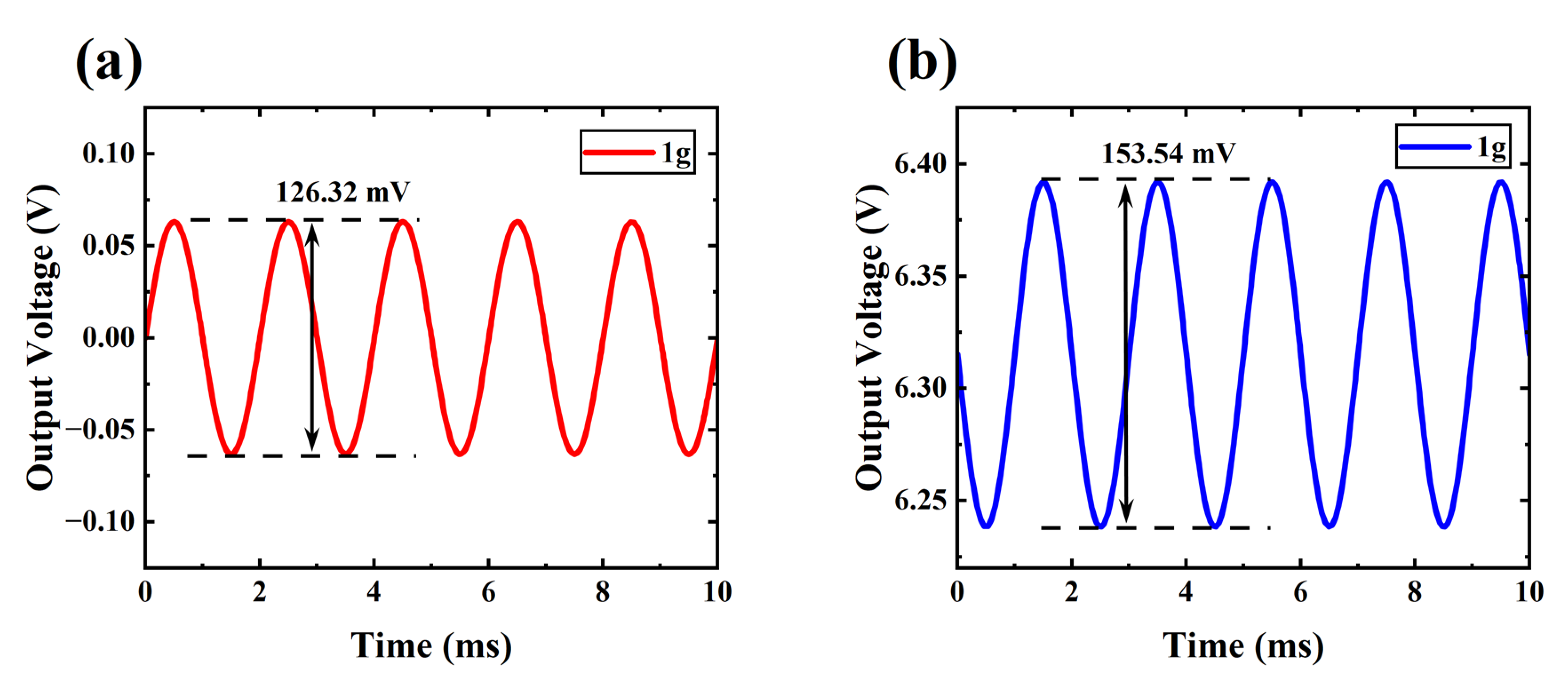
3.1. Sensitivity Adjustment Through Parameter Modifications

As per Equation (8), the output voltage of the piezo-VFETs is a function of VDD and RL, demonstrating the potential controllability over the output voltage of the artificial mechanoreceptor, which could be considered a significant advantage of integrating piezoelectric MEMS sensors with VFETs. In detail, for a given ΔVgs, the amplification ratio of the piezoelectric potential, i.e., ΔVout/ΔVgs, can be optimized by selecting appropriate load resistors RL and external DC power supplies VDD. This amplification ratio can also be referred to as the sensitivity of the piezo-VFETs.
Figure 3 illustrates the sensitivity curves of piezo-VFETs with various VDD and RL. In general, the sensitivity curve of a sensor requires a high degree of linearity. Compared to capacitive MEMS sensors, one of the primary advantages of piezoelectric MEMS sensors is their ability to maintain high linearity while also achieving high sensitivity, which has contributed to their increasing popularity in recent years [47,48,49,54,56]. Both Figure 3a,b can be divided into three distinct segments. The linear fitting of these segments shows that the sensitivity adjustment of the proposed piezo-VFETs by VDD and RL is highly linear.
Figure 3a shows the ratio versus RL with a constant input signal ΔVgs and VDD. The entire curve can be divided into three regions. Initially, before 2.5 MΩ, the curve exhibits a rapid rising phase, where sensitivity to the RL changes significantly. The second region, from 2.5 MΩ to 10 MΩ, represents the sub-saturation zone, where the sensitivity to RL changes gradually diminishes and the trend becomes less pronounced. Finally, beyond 10 MΩ, the sensitivity to RL changes becomes increasingly negligible and stabilizes.
Figure 3b illustrates the sensitivity curve as a function of VDD with a fixed Vgs and RL of 10 MΩ. Similar to Figure 3a, the sensitivity curve exhibits three distinct phases as VDD varies. Firstly, before 2.5 V, the sensitivity curve exhibits a rapid increase, with a significant rise in sensitivity to VDD. In the second region, ranging from 2.5 V to 15 V, the curve enters a sub-saturation zone. Within this range, the sensitivity response to changes in VDD gradually diminishes, and the trend becomes less pronounced. Finally, when VDD exceeds 15 V, the sensitivity to its variations becomes exceedingly minor and stabilizes.
As shown in Figure 3, the variations in VDD and RL have different degrees of impact on the sensitivity, which is reflected by the slope differences between each segment in Figure 3a,b. Across all three segments, the slope of the sensitivity curve concerning RL is consistently greater than that of VDD. Specifically, in the first segment, the slope for RL exceeds that for VDD by approximately 80.56%; in the second segment, it is around 37.5% higher; and in the third segment, it is about 25% greater. This difference suggests that, in practical applications, selecting and optimizing RL is more critical than adjusting VDD to achieve optimal performance and stability of the piezo-VFETs.
Resistive components unavoidably generate Johnson-Nyquist noise [57], which is directly proportional to the resistance value. Consequently, the magnitude of system noise is directly proportional to the system resistance. Additionally, the power consumption of the system, influenced by VDD, must also be taken into consideration. Therefore, in practical applications, it is essential to balance sensitivity, noise, and power consumption by selecting appropriate values of VDD and RL to achieve optimal system performance.

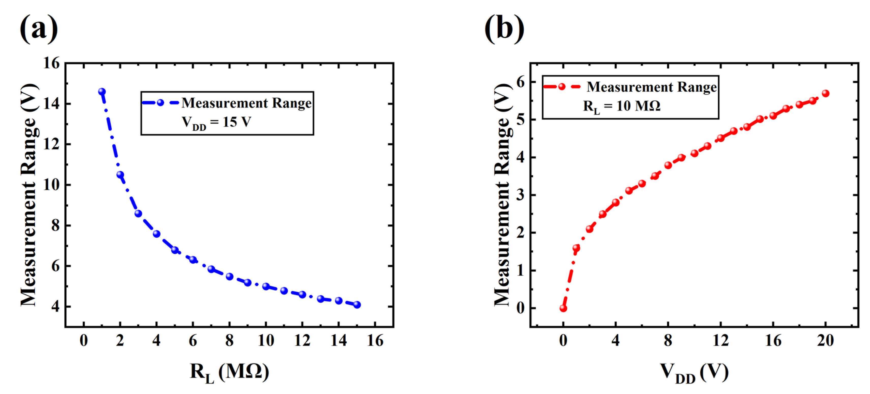
3.2. Measurement Range Adjustable from the Power Supply and Load Resistance

Generally, the linear measurement range is a critical performance parameter for MEMS sensors. The artificial mechanoreceptors based on the piezo-VFETs proposed here work around the static point of Vgs = 0. Its measurement range of mechanical signals is mainly determined by the linearity of the Ids-Vgs curve of the VFET design in Figure 1. In the transfer characteristic curves of the proposed VFET, as shown in Figure 1f, the variation of Ids with Vgs can be broadly divided into two segments with different slopes, where the inflection point between these two segments corresponds not only to the VFET’s threshold voltage but also to the measurement range of the piezo-VFETs. According to Equation (8), a change in Vgs (ΔVgs) results in a corresponding change in Ids (ΔIds). However, since the mechanical signals ΔVgs generated by most piezoelectric MEMS sensors are smaller than Vds [39,47,48,49,51,53,54], the change in Ids due to Vgs is negligible. Consequently, the measurement range of piezo-VFETs can be approximately determined based on Figure 1f. In this figure, different Vds values lead to different inflection points, altering the measurement range of piezo-VFETs.
As inferable from the discussion above, the linear measurement range of an artificial mechanoreceptor proposed in this paper is also affected by RL and VDD, both of which control the detail Vds of the VFET. Figure 4a shows the relationship between the measurement range and RL under a VDD of 15 V, illustrating that the measurement range of piezo-VFETs decreases as RL increases. Additionally, as discussed in Section 3.1, while an increase in RL leads to a rise in sensitivity, it also inevitably causes an increase in the overall noise of the piezo-VFETs. This implies that in practical applications, a balance must be struck between measurement range, noise, and sensitivity to select the appropriate load resistor, thereby maximizing overall performance.
Figure 4b illustrates the measurement range curve as a function of VDD with RL of 10 MΩ. Unlike the influence of RL on measurement range, the measurement range increases with the rise of VDD. Moreover, as noted in the discussion of the relationship between VDD and sensitivity in Section 3.1, increasing VDD can enhance sensitivity within certain limits, but this also inevitably increases the overall power consumption of the system. Therefore, selecting the appropriate RL and VDD based on different application requirements is necessary to achieve optimal performance.

3.3. Impact of VFET Array on the Characteristics of the Piezo-VFETs

As mentioned earlier, forming VFET into arrays can effectively increase the overall operational current. According to Equation (8), for given VDD and RL, (given VDD = 15 V and RL = 10 MΩ), changes in Ids will also affect the output voltage Vout. Figure 5a illustrates the relationship between the number of source electrodes and the sensitivity and measurement range of piezo-VFETs. As shown in Figure 5a, with the increase in the number of source electrodes, the overall output sensitivity of piezo-VFETs also increases, while the measurement range decreases correspondingly. As the number of source electrodes increases, the total current Ids rise under the same external bias conditions, leading to more pronounced changes in output voltage, thereby enhancing sensitivity. This phenomenon occurs because the increase in source electrodes results in each electrode contributing more current. The cumulative effect makes the output signal more responsive to input changes.
Simultaneously, according to Equation (8), when Ids increases, Vout decreases. This voltage drop inhibits further increases in Ids, thereby forming a negative feedback loop, as shown in Figure 5b. In this process, the system automatically adjusts to reach a new equilibrium point for Vout (Vds). A change in this equilibrium point leads to a reduction in the measurement range. This is due to the rapid rise in current Ids with the increase in the number of source electrodes causing Vout to reach equilibrium more quickly, thus limiting the variable range of Vgs. This negative feedback mechanism ensures system stability. It also implies a trade-off between sensitivity and measurement range in practical applications. To achieve optimal performance, the appropriate VFET array configuration must be selected based on specific application requirements. In applications requiring high sensitivity, more electrodes may be needed. In applications requiring a larger measurement range, the number of source electrodes should be carefully controlled.

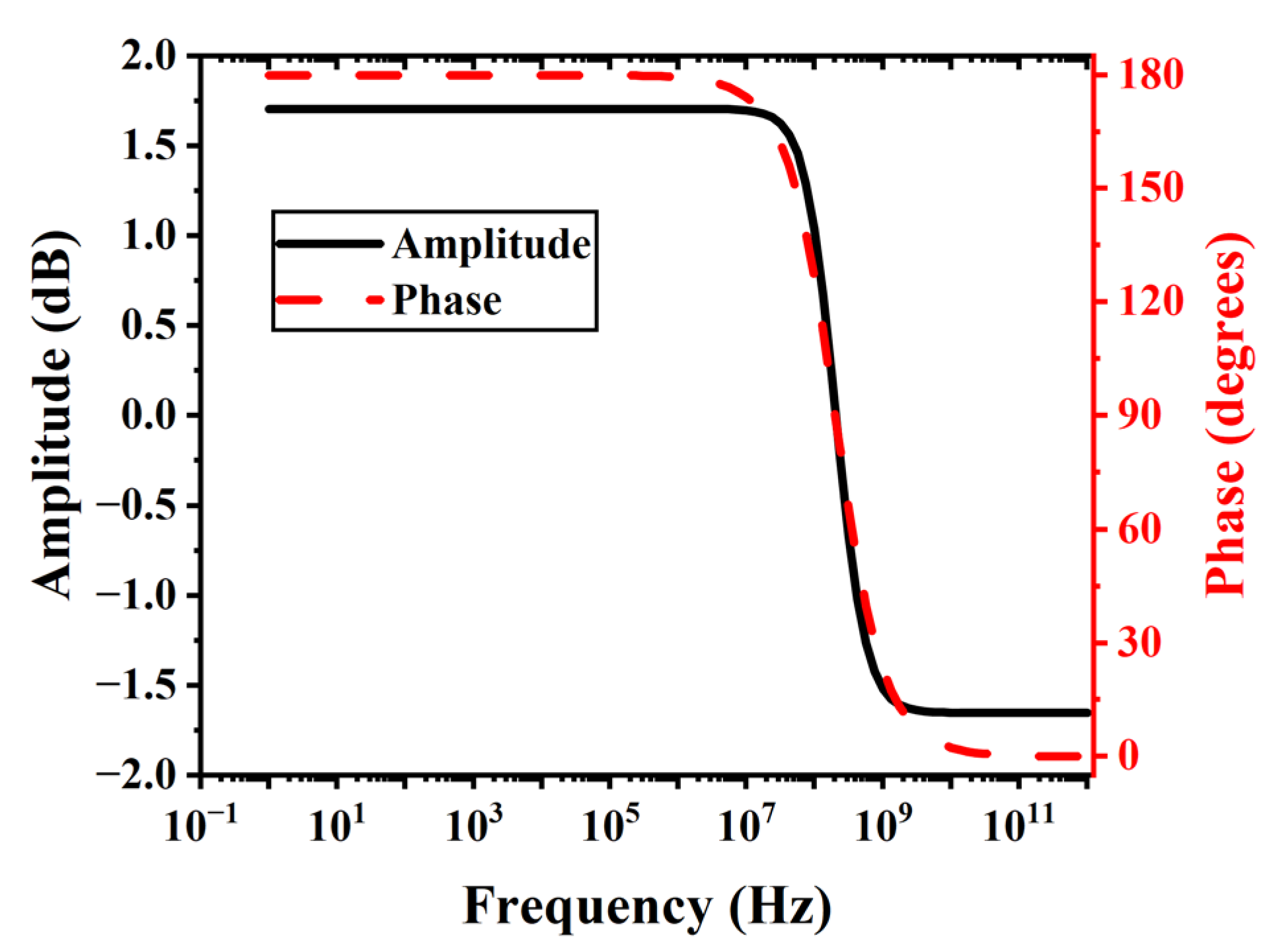
3.4. Bandwidth of the Piezo-VFETs

Due to the ballistic transport of electrons within its internal vacuum channel, VFET exhibits excellent frequency response characteristics [4,5,8,15,21]. When integrated with piezoelectric MEMS sensors to amplify the electrical signal output from piezoelectric MEMS sensors, the frequency response characteristic curve of the VFET circuit determines the bandwidth of the entire system. Ideally, the flat band of the VFET circuit should encompass the mechanical resonance frequency of the piezoelectric MEMS sensors. This ensures that the operational bandwidth of the entire system is not adversely affected by the integration. Figure 6 depicts the simulated frequency response characteristic curve (Bode plot) of the piezo-VFETs at VDD = 15 V and RL = 10 MΩ. It can be seen that the flat band of the VFET circuit covers frequencies below 10 MHz. Table 1 lists the frequency bandwidth of representative piezoelectric MEMS sensors. As inferable from Table 1, the VFET circuit has a flat band encompassing the mechanical resonance frequency of most piezoelectric MEMS sensors, demonstrating that the piezo-VFETs proposed in this paper can be effectively used to couple with piezoelectric MEMS sensors to form artificial mechanoreceptors for sensing purposes [47,48,49,50,51,56,58,59,60].

3.5. Noise of the Piezo-VFETs as an Artificial Mechanoreceptor

For the piezo-VFETs proposed in this paper, the primary noise source is the piezoelectric sensing unit. The noise of the piezoelectric sensing unit can be written as follows [62]:
v n = 4 k B T ω 0 Q T 2 C 2 m Q + η ω C V n = v n Δ f
Here, vn represents the total voltage noise density of the piezoelectric sensing unit (V/√Hz), kB is Boltzmann’s constant (1.38 × 10⁻²³ J/K), T is the absolute temperature (K), ω0 is the angular mechanical resonant frequency, QT is the piezoelectric sensing unit’s charge sensitivity, C is the total capacitance of the piezoelectric sensing unit, m is the mass (kg), Q is the quality factor, η is the dissipation constant of the piezoelectric material, ω is the angular frequency, Vn is the total voltage noise (V), and Δf is the bandwidth in hertz (Hz) over which the noise is measured.
Based on Equation (9), the noise reflected in the Vout of the piezo-VFETs is:
V o u t = V D D A α β 2 V n + V g s + V d s μ 2 d 2 φ exp B d φ 3 / 2 β V n + V g s + V d s μ × R L
The noise generated by the piezoelectric sensing unit is coupled to the VFETs through the input voltage, subsequently affecting the overall output noise level of the piezo-VFETs. This process indicates that the noise performance of the piezoelectric sensing unit directly determines the overall noise behavior of the piezo-VFETs, particularly in high-sensitivity applications where noise amplification effects are more pronounced. To mitigate the noise issue, structural optimization of the piezoelectric sensing unit is crucial. Adjustments in the design and material selection of the piezoelectric unit can reduce intrinsic noise. For instance, improving the uniformity of the piezoelectric material can help minimize noise coupling into the VFETs. Additionally, electromagnetic shielding and incorporating appropriate filtering circuits can further reduce noise in the entire system. In the final integration of the VFETs and piezoelectric sensing unit, the use of appropriate vacuum packaging to place the system in an optimal working environment can further reduce the impact of external environmental noise on the piezo-VFETs, thereby enhancing the overall stability and measurement accuracy of the system.

4. Application Potential of Piezo-VFETs as Artificial Mechanoreceptors for Sensing Purposes

The characteristics of the newly proposed piezo-VFETs revealed in Section 3 indicate its promising potential. For further clarification, this section uses polymeric piezoelectric accelerometers in existing studies as examples to show the significance of the piezo-VFETs proposed in this paper.

4.1. Increment of Sensitivity, Bandwidth, and Degree of Miniaturization

In 2023, Ge et al. proposed a PVDF-based piezoelectric MEMS accelerometer with a voltage sensitivity of 126.32 mV/g (1g = 9.8 m/s2) [47]. If this polymer piezoelectric accelerometer is interfaced with a VFET array in Figure 1 to form an artificial mechanoreceptor based on piezo-VFETs (VDD = 15 V and RL = 10 MΩ), as shown in Figure 7, the voltage output is increased by 1.216 times.
Traditional piezoelectric MEMS sensors have their sensitivity positively related to the planar dimensions of the piezoelectric layers sandwiched by electrodes [47,49,50,58,60]. For polymeric piezoelectric accelerometers such as the ones of Ge et al., due to the inferior piezoelectric properties of polymers, their accelerometers have very limited degrees of miniaturization and bandwidth. As indicated by the sensitivity increment in Figure 7, using such polymeric piezoelectric MEMS sensors in the newly proposed piezo-VFETs allows MEMS devices to achieve further miniaturization and, correspondingly, increased bandwidth while maintaining consistent sensitivity. Moreover, compared with the classic piezoelectric MEMS readout circuit based on charge amplifiers using operational amplifiers, the complexity of the readout circuit of the piezo-VFETs proposed in this paper is also reduced [47,48].

4.2. Reduced Power Consumption than Piezo-FETs

VFETs inherently have a lower continuous current than most solid-state field effect transistors (FETs), which translates to a distinct advantage in power consumption, making the integration of piezoelectric MEMS sensors with VFETs more advantageous than with other solid-state FETs.
For the VFET array combined with the polymer piezoelectric MEMS accelerometers of Ge et al., simulations estimate its static power consumption to be 83.7 μW at VDD = 15 V and RL = 10 MΩ. Table 2 summarizes the continuous current, corresponding power consumption, fabrication complexity, and cost of piezo-FETs as sensors in existing studies [33,34,35,36,37,38,63,64,65,66], with a comparison to our piezo-VFETs, using Ge et al.’s polymer piezoelectric MEMS accelerometers as an example. We evaluate the fabrication complexity based on its compatibility with modern integrated circuits and Complementary Metal-Oxide-Semiconductor (CMOS) processes, as well as the integration difficulty with piezoelectric sensing units. Additionally, the fabrication cost is assessed through the complexity of the fabrication process, the difficulty of large-scale production, and material costs.
As shown in Table 2, although some solid-state FETs fabricated with advanced materials such as graphene exhibit lower power consumption than VFETs, when silicon is used as the semiconductor material, the continuous current of such solid-state FETs is generally in the milliampere range, and their power consumption is in the microwatt range. In contrast, the continuous current of our silicon based VFET is reduced by an order of magnitude, highlighting its advantage in power efficiency. Additionally, solid-state FETs suffer from poor thermal stability, with their continuous current significantly affected by temperature environments. Although directly integrating the piezoelectric sensing unit as part of solid-state FETs, such as using it as the gate of FETs, allows for higher miniaturization, this approach faces more complex fabrication processes and is challenging to achieve large-scale production. Moreover, stability and reliability remain concerns. Separating the fabrication of the piezoelectric sensing unit and VFETs can avoid compatibility issues in the fabrication process, thus improving the stability of piezo-VFETs as artificial mechanoreceptors and reducing manufacturing costs. Overall, this highlights the clear advantages of VFETs in terms of low power consumption. Thermal stability and fabrication cost make them an ideal choice for integration with piezoelectric MEMS sensors.

5. Method

All the data presented in this study were obtained through simulations, using a combined approach with the finite element electromagnetic simulation software CST Studio Suite (version 2022) and the circuit simulation software LTspice (version XVII). First, the particle tracking solver in CST Studio was utilized to design the VFET structure and calculate its electrical characteristics. The simulation environment was set to a complete vacuum to eliminate the influence of the external environment, thereby achieving more accurate results. The Fowler-Nordheim (F-N) field emission model was employed in the CST Studio Suite, and Equation (1) was simplified as follows:
J F N = a F N E 2 exp b F N / E
Based on the field emission parameters of silicon-based material obtained from our previous experiments, the values of aFN = 6.0 × 10⁻⁹ (unit: A/V2) and bFN = 2.56 × 10⁷ (unit: V/m) were used in the simulation. Subsequently, the VFET structure parameters, I-V characteristics, and parasitic parameters such as inter-electrode capacitance was extracted from CST Studio Suite and imported into LTspice to construct the VFET equivalent circuit model. This model facilitated further analysis of the piezo-VFETs’ characteristics.

6. Conclusions

In this paper, a novel vacuum field emission transistor design was proposed. It was customized to integrate piezoelectric MEMS sensors to form piezo-VFETs for artificial mechanoreceptors as bionic electronics. Theoretical studies and simulations were conducted to validate the feasibility of such a configuration and to demonstrate its characteristics. The corresponding results reveal that the sensitivity and measurement range of the newly proposed piezo-VFETs can be optimized by adjusting the load resistance and DC power supply. Additionally, the simulation results indicated that the sensitivity and measurement range of piezo-VFETs can be effectively tuned by varying the number of source electrodes in the VFET array. Moreover, the superior high-frequency performance of the VFET was found to align with the flat-band resonance frequency of the MEMS devices, ensuring that the integration of the two components is not constrained by bandwidth limitations. In a case study based on polymeric piezoelectric MEMS accelerometers interfaced with the classic charge amplifier circuits, it is demonstrated that the sensitivity of piezo-VFETs was increased by approximately 1.2 times compared to the original piezoelectric MEMS sensor with a significantly simplified readout circuit. In addition, the simulation in this paper also demonstrates that, compared to piezo-FETs using field-effect transistors, the piezo-VFETs illustrate a significant advantage in power consumption. This paper underscores the significant potential of piezoelectric VFETs in high-performance sensor applications, laying a solid foundation for the broader integration of piezoelectric VFETs in the future.

Supplementary Materials

The following supporting information can be downloaded at: https://www.mdpi.com/article/10.3390/s24206764/s1, Figure S1: (a) Structure parameters of proposed VFET, highlighting the gate-source distance (dgs), drain-source distance (dds), and gate radius (rg). (b) Transfer characteristic curves with various dgs (Vds = 20 V, and rg = 100 nm). Electric field distribution at source tip for different dgs values: (c)dgs = 100 nm, (d) dgs = 25 nm, (e) dgs = −25 nm, and (f) dgs = −100 nm.; Figure S2: (a) The structure parameters of the proposed VFET highlight the gate-source distance (dgs = 100 nm), drain-source distance (dds = 200 nm), and gate radius. (b) Transfer characteristic curves with various combinations of gate radii (Vds = 20 V, and dgs = 100 nm); Figure S3: Schematics (not to scale) showing the Outlines of the fabrication process of the proposed VFET.

Author Contributions

Conceptualization, C.G. and Y.C.; methodology, C.G. and Y.C.; software, Y.C.; validation, C.G., Y.C. and J.X.; formal analysis, Y.C.; investigation, D.Y.; resources, C.G. and J.X.; data curation, Y.C.; writing—original draft preparation, Y.C. and C.G.; writing—review and editing, C.G., Y.C. and J.X.; visualization, D.Y and Z.L.; supervision, Z.L. and J.X.; project administration, C.G., Y.C. and J.X.; funding acquisition, J.X. All authors have read and agreed to the published version of the manuscript.

Funding

This research was funded by the National Natural Science Foundation of China (Grant No. 92264103, Grant No. 62401399) and in part by the National Key Research and Development Program of China (Grant No. 2022YFB4401301).

Institutional Review Board Statement

Not applicable.

Informed Consent Statement

Not applicable.

Data Availability Statement

All data that support the findings of this study are included within the article (and any Supplementary Materials).

Conflicts of Interest

The authors declare no conflicts of interest.

References

  1. Armstrong, C.M.; Kowalczyk, R.; Zubyk, A.; Berg, K.; Meadows, C.; Chan, D.; Schoemehl, T.; Duggal, R.; Hinch, N.; True, R.B.; et al. A Compact Extremely High Frequency MPM Power Amplifier. IEEE Trans. Electron Devices 2018, 65, 2183–2188. [Google Scholar] [CrossRef]
  2. Pan, P.; Tang, Y.; Bian, X.; Zhang, L.; Lu, Q.; Li, Y.; Feng, Y.; Feng, J. A G-Band Traveling Wave Tube With 20 W Continuous Wave Output Power. IEEE Electron Device Lett. 2020, 41, 1833–1836. [Google Scholar] [CrossRef]
  3. Symons, R.S. Tubes: Still vital after all these years. IEEE Spectrum 1998, 35, 52–63. [Google Scholar] [CrossRef]
  4. De Rose, L.B.; Jones, W.M.; Scherer, A. Lateral nanoscale field emission comb for frequency mixing. Appl. Phys. Lett. 2023, 123, 013505. [Google Scholar] [CrossRef]
  5. Han, J.-W.; Oh, J.S.; Meyyappan, M. Vacuum nanoelectronics: Back to the future?—Gate insulated nanoscale vacuum channel transistor. Appl. Phys. Lett. 2012, 100, 213505. [Google Scholar] [CrossRef]
  6. Fan, L.; Zhao, B.; Chen, B.; Ma, Y.; Bi, J.; Zhao, F. Radiation Immune-Planar Two-Terminal Nanoscale Air Channel Devices toward Space Applications. ACS Appl. Nano Mater. 2023, 6, 22080–22087. [Google Scholar] [CrossRef]
  7. Han, J.-W.; Moon, D.-I.; Meyyappan, M. Nanoscale Vacuum Channel Transistor. Nano Lett. 2017, 17, 2146–2151. [Google Scholar] [CrossRef]
  8. Wei, Y.; Chen, F.; Huang, R.; Zhao, J.; Zhao, H.; Wang, J.; Li, M.; Zhang, J. Fast Response GaN Nanoscale Air Channel Diodes with Highly Stable 10 mA Output Current toward Wafer-Scale Fabrication. Adv. Sci. 2023, 10, 2206385. [Google Scholar] [CrossRef]
  9. Stoner, B.R.; Glass, J.T. Nothing is like a vacuum. Nat. Nanotechnol. 2012, 7, 485–487. [Google Scholar] [CrossRef]
  10. de Heer, W.A.; Châtelain, A.; Ugarte, D. A Carbon Nanotube Field-Emission Electron Source. Science 1995, 270, 1179–1180. [Google Scholar] [CrossRef]
  11. Hsu, S.H.; Kang, W.P.; Raina, S.; Huang, J.H. Nanodiamond vacuum field emission device with gate modulated triode characteristics. Appl. Phys. Lett. 2013, 102, 203105. [Google Scholar] [CrossRef]
  12. Nirantar, S.; Patil, B.; Tripathi, D.C.; Sethu, N.; Narayanan, R.V.; Tian, J.; Bhaskaran, M.; Walia, S.; Sriram, S. Metal-Air Field Emission Devices—Nano Electrode Geometries Comparison of Performance and Stability. Small 2022, 18, 2203234. [Google Scholar] [CrossRef] [PubMed]
  13. Shih, P.-C.; Perozek, J.; Akinwande, A.I.; Palacios, T. Anode-Integrated GaN Field Emitter Arrays for Compact Vacuum Transistors. IEEE Electron Device Lett. 2023, 44, 1895–1898. [Google Scholar] [CrossRef]
  14. Wang, X.; Zheng, C.; Xue, T.; Shen, Z.; Long, M.; Wu, S. Nanoscale Vacuum Field Emission Triode with a Double Gate Structure. IEEE Electron Device Lett. 2022, 43, 292–295. [Google Scholar] [CrossRef]
  15. Xu, J.; Hu, H.; Yang, W.; Li, C.; Shi, Y.; Shi, Y.; Wang, Q.; Zhang, X. Nanoscale vacuum channel transistor with in-plane collection structure. Nanotechnology 2020, 31, 065202. [Google Scholar] [CrossRef]
  16. Zhang, Y.; Zhang, G.; Zhan, F.; He, Y. Planar nanoscale vacuum channel transistors based on resistive switching. Nanotechnology 2024, 35, 215205. [Google Scholar] [CrossRef]
  17. Han, J.-W.; Seol, M.-L.; Moon, D.-I.; Hunter, G.; Meyyappan, M. Nanoscale vacuum channel transistors fabricated on silicon carbide wafers. Nat. Electron. 2019, 2, 405–411. [Google Scholar] [CrossRef]
  18. Nirantar, S.; Ahmed, T.; Ren, G.; Gutruf, P.; Xu, C.; Bhaskaran, M.; Walia, S.; Sriram, S. Metal–Air Transistors: Semiconductor-Free Field-Emission Air-Channel Nanoelectronics. Nano Lett. 2018, 18, 7478–7484. [Google Scholar] [CrossRef]
  19. Wu, G.; Wei, X.; Zhang, Z.; Chen, Q.; Peng, L. A Graphene-Based Vacuum Transistor with a High ON/OFF Current Ratio. Adv. Funct. Mater. 2015, 25, 5972–5978. [Google Scholar] [CrossRef]
  20. Heo, S.J.; Shin, J.H.; Jun, B.O.; Jang, J.E. Vacuum Tunneling Transistor with Nano Vacuum Chamber for Harsh Environments. ACS Nano 2023, 17, 19696–19708. [Google Scholar] [CrossRef]
  21. Xu, J.; Qin, Y.; Shi, Y.; Shi, Y.; Yang, Y.; Zhang, X. Design and circuit simulation of nanoscale vacuum channel transistors. Nanoscale Adv. 2020, 2, 3582–3587. [Google Scholar] [CrossRef] [PubMed]
  22. Chang, W.-T.; Cheng, M.-C.; Chuang, T.-Y.; Tsai, M.-Y. Field Emission Air-Channel Devices as a Voltage Adder. Nanomaterials 2020, 10, 2378. [Google Scholar] [CrossRef] [PubMed]
  23. Han, J.-W.; Seol, M.-L.; Kim, J.; Meyyappan, M. Nanoscale Complementary Vacuum Field Emission Transistor. ACS Appl. Nano Mater. 2020, 3, 11481–11488. [Google Scholar] [CrossRef]
  24. Bhattacharya, R.; Han, J.W.; Browning, J.; Meyyappan, M. Complementary Vacuum Field Emission Transistor. IEEE Trans. Electron. Devices 2021, 68, 5244–5249. [Google Scholar] [CrossRef]
  25. Zhu, J.; Yao, K.; Dong, X.S.; Huang, Q.W.; Liu, R.H. Pull-in behavior of electrostatically actuated stepped microbeams. Int. J. Mod. Phys. B 2018, 32, 1850180. [Google Scholar] [CrossRef]
  26. Chen, Y.B.; Yan, Z. Investigation of pull-in behaviors of a nanoswitch tuned by piezoelectric and flexoelectric effects. Int. J. Mech. Sci. 2019, 161, 105032. [Google Scholar] [CrossRef]
  27. Cai, T.; Fang, Y.M.; Fang, Y.L.; Li, R.Z.; Yu, Y.; Huang, M.Y. Electrostatic pull-in application in flexible devices: A review. Beilstein J. Nanotechnol. 2022, 13, 390–403. [Google Scholar] [CrossRef]
  28. Dehkordi, M.F.; Beni, Y.T.; Dashtaki, P.M.; Vanani, S.M.F. Effect of flexoelectricity on the Pull-in instability of beam-type NEMS. Eng. Anal. Bound. Elem. 2023, 155, 87–107. [Google Scholar] [CrossRef]
  29. French, A.S.; Torkkeli, P.H. Chapter 36—Sensory Receptors and Mechanotransduction. In Cell Physiology Source Book, 4th ed.; Sperelakis, N., Ed.; Academic Press: San Diego, CA, USA, 2012; pp. 633–647. [Google Scholar]
  30. Yogeswaran, N.; Hosseini, E.S.; Dahiya, R. Graphene Based Low Voltage Field Effect Transistor Coupled with Biodegradable Piezoelectric Material Based Dynamic Pressure Sensor. ACS Appl. Mater. Interfaces 2020, 12, 54035–54040. [Google Scholar] [CrossRef]
  31. Wang, J.C.; Jiang, Y.P.; Lin, C.H.; Chan, S.H.; Wu, M.C. Enhanced piezoelectric tactile sensing behaviors of high-density and low-damage CF4-plasma-treated IGZO thin-film transistors coated by P(VDF-TrFE) copolymers. Sens. Actuator A Phys. 2020, 304, 9. [Google Scholar] [CrossRef]
  32. Wang, J.; Jiang, J.F.; Zhang, C.C.; Sun, M.Y.; Han, S.W.; Zhang, R.T.; Liang, N.; Sun, D.H.; Liu, H. Energy-efficient, fully flexible, high-performance tactile sensor based on piezotronic effect: Piezoelectric signal amplified with organic field-effect transistors. Nano Energy 2020, 76, 8. [Google Scholar] [CrossRef]
  33. Wang, F.L.; Jiang, J.F.; Liu, Q.L.; Zhang, Y.; Wang, J.J.; Wang, S.H.; Han, L.; Liu, H.; Sang, Y.H. Piezopotential gated two-dimensional InSe field-effect transistor for designing a pressure sensor based on piezotronic effect. Nano Energy 2020, 70, 8. [Google Scholar] [CrossRef]
  34. Meng, Z.M.; Zhang, H.; Zhu, M.; Wei, X.Y.; Cao, J.P.; Murtaza, I.; Ali, M.U.; Meng, H.; Xu, J.Y. Lead Zirconate Titanate (a piezoelectric ceramic)-Based thermal and tactile bimodal organic transistor sensors. Org. Electron. 2020, 80, 5. [Google Scholar] [CrossRef]
  35. Zhu, M.J.; Inomata, N.; Adachi, N.; Sakurai, A.; Nomura, M.; Ono, T. High-Gauge Factor Strain Sensor Based on Piezoelectric Aluminum Nitride Coupled to MOSFET. IEEE Sens. J. 2019, 19, 3626–3632. [Google Scholar] [CrossRef]
  36. Sung, M.; Shin, K.; Moon, W. A micro-machined hydrophone employing a piezoelectric body combined on the gate of a field-effect transistor. Sens. Actuator A Phys. 2016, 237, 155–166. [Google Scholar] [CrossRef]
  37. Ueda, M.; Kaneko, Y.; Nishitani, Y.; Omote, A. Battery-less shock-recording device consisting of a piezoelectric sensor and a ferroelectric-gate field-effect transistor. Sens. Actuator A Phys. 2015, 232, 75–83. [Google Scholar] [CrossRef]
  38. Sung, M.; Shin, K.; Moon, W. A new transduction mechanism for hydrophones employing piezoelectricity and a field-effect transistor. Sens. Actuator A Phys. 2015, 233, 557–568. [Google Scholar] [CrossRef]
  39. Ai, C.P.; Zhao, X.F.; Wen, D.Z. Characteristics Research of a High Sensitivity Piezoelectric MOSFET Acceleration Sensor. Sensors 2020, 20, 14. [Google Scholar] [CrossRef]
  40. Ellis, R.K. Fowler-Nordheim emission from non-planar surfaces. IEEE Electron Device Lett. 1982, 3, 330–332. [Google Scholar] [CrossRef]
  41. Forbes, R.G.; Deane, J.H.B. Reformulation of the standard theory of Fowler–Nordheim tunnelling and cold field electron emission. Proc. R. Soc. A. 2007, 463, 2907–2927. [Google Scholar] [CrossRef]
  42. Kosmahl, H.G. Analytic evaluation of field emission enhancement factors for ellipsoidal cones and elliptic cross-section wedges. IEEE Trans. Electron Devices 1991, 38, 1534–1537. [Google Scholar] [CrossRef]
  43. Lenzlinger, M.; Snow, E.H. Fowler-Nordheim Tunneling into Thermally Grown SiO2. J. Appl. Phys. 1969, 40, 278–283. [Google Scholar] [CrossRef]
  44. Fowler, R.H.; Nordheim, L. Electron Emission in Intense Electric Fields. Proc. R. Soc. Lond. Ser. A Contain. Pap. A Math. Phys. Character 1928, 119, 173–181. [Google Scholar]
  45. Han, J.W.; Oh, J.S.; Meyyappan, M. Cofabrication of Vacuum Field Emission Transistor (VFET) and MOSFET. IEEE Trans. Nanotechnol. 2014, 13, 464–468. [Google Scholar] [CrossRef]
  46. Wisitsora-At, A.; Kang, W.P.; Davidson, J.L.; Li, C.; Kerns, D.V.; Howell, M. Modeling of the transistor characteristics of a monolithic diamond vacuum triode. J. Vac. Sci. Technol. B Microelectron. Nanometer Struct. Process. Meas. Phenom. 2003, 21, 1665–1670. [Google Scholar] [CrossRef]
  47. Ge, C.; Cretu, E. A polymeric piezoelectric MEMS accelerometer with high sensitivity, low noise density, and an innovative manufacturing approach. Microsyst. Nanoeng. 2023, 9, 151. [Google Scholar] [CrossRef]
  48. Ge, C.; Cretu, E. Polymeric piezoelectric accelerometers with high sensitivity, broad bandwidth, and low noise density for organic electronics and wearable microsystems. Microsyst. Nanoeng. 2024, 10, 61. [Google Scholar] [CrossRef]
  49. Gong, X.; Kuo, Y.-C.; Zhou, G.; Wu, W.-J.; Liao, W.-H. An aerosol deposition based MEMS piezoelectric accelerometer for low noise measurement. Microsyst. Nanoeng. 2023, 9, 23. [Google Scholar] [CrossRef]
  50. Hewa-Kasakarage, N.N.; Kim, D.; Kuntzman, M.L.; Hall, N.A. Micromachined Piezoelectric Accelerometers via Epitaxial Silicon Cantilevers and Bulk Silicon Proof Masses. J. Microelectromech. Syst. 2013, 22, 1438–1446. [Google Scholar] [CrossRef]
  51. Lee, Y.-C.; Tsai, C.-C.; Li, C.-Y.; Liou, Y.-C.; Hong, C.-S.; Chu, S.-Y. Fabrication and function examination of PZT-based MEMS accelerometers. Ceram. Int. 2021, 47, 24458–24465. [Google Scholar] [CrossRef]
  52. Liu, Y.; Hu, B.; Cai, Y.; Liu, W.; Tovstopyat, A.; Sun, C. A Novel Tri-Axial Piezoelectric MEMS Accelerometer with Folded Beams. Sensors 2021, 21, 453. [Google Scholar] [CrossRef] [PubMed]
  53. Udvardi, P.; Radó, J.; Straszner, A.; Ferencz, J.; Hajnal, Z.; Soleimani, S.; Schneider, M.; Schmid, U.; Révész, P.; Volk, J. Spiral-Shaped Piezoelectric MEMS Cantilever Array for Fully Implantable Hearing Systems. Micromachines 2017, 8, 311. [Google Scholar] [CrossRef] [PubMed]
  54. Yang, C.; Hu, B.; Lu, L.; Wang, Z.; Liu, W.; Sun, C. A Miniaturized Piezoelectric MEMS Accelerometer with Polygon Topological Cantilever Structure. Micromachines 2022, 13, 1608. [Google Scholar] [CrossRef] [PubMed]
  55. Pogorelov, E.G.; Zhbanov, A.; Chang, Y.-C.J.U. Field enhancement factor and field emission from a hemi-ellipsoidal metallic needle. Ultramicroscopy 2008, 109, 373–378. [Google Scholar] [CrossRef]
  56. Debnath, B.; Kumar, R. Single-axis low acceleration sensing using an enhanced piezoelectric vibration energy harvester. Microsyst. Technol. 2021, 27, 3171–3181. [Google Scholar] [CrossRef]
  57. Nyquist, H. Thermal Agitation of Electric Charge in Conductors. Phys. Rev. 1928, 32, 110–113. [Google Scholar] [CrossRef]
  58. Yang, T.; Wang, Q.; Zhang, Z.; Liao, Z.; Zhao, Y.; Li, Y.; Zang, J.; Gao, R.; Cui, D.; Xue, C. Design and Implementation of 6 × 6 Array Piezoelectric AlN Hydrophone with High Sensitivity. IEEE Sens. J. 2021, 21, 26615–26623. [Google Scholar] [CrossRef]
  59. Minh, L.V.; Hara, M.; Kuwano, H. Lead-Free (K,Na)NbO3 Impact-Induced-Oscillation Microenergy Harvester. J. Microelectromech. Syst. 2015, 24, 1887–1895. [Google Scholar] [CrossRef]
  60. Ali, W.R.; Prasad, M. Piezoelectric Based MEMS Acoustic Sensor for Wide Frequency Applications. IEEE Sens. J. 2021, 21, 27352–27360. [Google Scholar] [CrossRef]
  61. Prasad, M.; Aditi; Khanna, V.K. Development of MEMS Acoustic Sensor with Microtunnel for High SPL Measurement. IEEE Trans. Ind. Electron. 2022, 69, 3142–3150. [Google Scholar] [CrossRef]
  62. Levinzon, F.A. Fundamental noise limit of piezoelectric accelerometer. IEEE Sens. J. 2004, 4, 108–111. [Google Scholar] [CrossRef]
  63. Dahiya, R.S.; Metta, G.; Valle, M.; Adami, A.; Lorenzelli, L. Piezoelectric Oxide Semiconductor Field Effect Transistor Touch Sensing Devices. Appl. Phys. Lett. 2009, 95, 3. [Google Scholar] [CrossRef]
  64. Maita, F.; Maiolo, L.; Minotti, A.; Pecora, A.; Ricci, D.; Metta, G.; Scandurra, G.; Giusi, G.; Ciofi, C.; Fortunato, G. Ultraflexible Tactile Piezoelectric Sensor Based on Low-Temperature Polycrystalline Silicon Thin-Film Transistor Technology. IEEE Sens. J. 2015, 15, 3819–3826. [Google Scholar] [CrossRef]
  65. Viola, F.A.; Spanu, A.; Ricci, P.C.; Bonfiglio, A.; Cosseddu, P. Ultrathin, Flexible and Multimodal Tactile Sensors Based on Organic Field-Effect Transistors. Sci. Rep. 2018, 8, 8. [Google Scholar] [CrossRef] [PubMed]
  66. Hsu, Y.J.; Jia, Z.; Kymissis, I. A Locally Amplified Strain Sensor Based on A Piezoelectric Polymer and Organic Field-Effect Transistors. IEEE Trans. Electron Devices 2011, 58, 910–917. [Google Scholar] [CrossRef]
Figure 1. Schematic structure of the proposed VFET: (a) overall view; (b) cross-sectional view with structural parameters; (c) schematic structure of the VFET array; (d) the drains current increases linearly with the number of source electrodes. Electrical characteristics of the 3 × 3 VFET array; (e) output characteristic curves; and (f) transfer characteristic curves.
Sensors 24 06764 g001
Figure 2. (a) Circuit schematic of piezoelectric VFET sensors (piezo-VFETs); and (b) the relationship between Vout and RL as derived from Equation (8) and as obtained from simulation (VDD = 10 V and Vgs = 0 V).
Sensors 24 06764 g002
Figure 3. (a) Sensitivity as a function of load resistance (RL) with a DC power supply voltage (VDD) of 20 V; and (b) sensitivity as a function of VDD with RL set to 10 MΩ.
Sensors 24 06764 g003
Figure 4. (a) Measurement range as functions of RL with VDD set at 15 V; and (b) measurement range as functions of VDD with and RL fixed at 10 MΩ.
Sensors 24 06764 g004
Figure 5. (a) Curves depicting sensitivity and measurement range vs. number of source electrodes (VDD = 15 V, RL = 10 MΩ); and (b) negative feedback loop (An arrow up refers to rise in current or voltage, while an arrow down refers to a fall in current or voltage.).
Sensors 24 06764 g005
Figure 6. Frequency response characteristic curve (Bode plot) of the piezo-VFETs.
Sensors 24 06764 g006
Figure 7. The output characteristic of PVDF-based piezoelectric MEMS accelerometers (a) piezo-VFETs; and (b) under a 1g acceleration (VDD = 15 V, RL = 10 MΩ).
Sensors 24 06764 g007
Table 1. The frequency bandwidth of representative piezoelectric MEMS sensors.
ResearchPiezoelectric
Material
Sensor
Types
BandwidthResonance
Frequency
Ali et al. [60]ZnOAcoustic sensor15 kHz78 kHz
Prasad et al. [61]ZnOAcoustic sensor8 kHz42.875 kHz
Minh et al. [59](K, Na) NbO3Energy harvester150 Hz3.094 kHz
Ge et al. [47]PVDFAccelerometer58.6 Hz128.95 Hz
Gong et al. [49]PZTAccelerometer200 Hz857.4 Hz
Yang et al. [58]AlNHydrophone2 kHz479 kHz
Table 2. The continuous current, corresponding power consumption, fabrication complexity, and cost of piezo-FETs as sensors in existing studies with a comparison to our piezo-VFETs.
ResearchersSensor
Types
Semiconductor MaterialContinuous
Current
SensitivityOperating
Voltage
Power
Consumption
Fabrication ComplexityCost
Dahiya et al. [63]TactileSilicon3~4 mA50 mV/N (Load: 100 kΩ)VSS = −5 V15~20 mWMiddleLow
Maita et al. [64]TactileSilicon~40 µA430 mV/N (Load: 270 kΩ)VDD = 20 V,
VG = 9 V
~0.8 mWMiddleLow
Viola et al. [65]TactilePolyethylene naphthalene (PEN)−3~−4 µA0.15 nA/kPaVDD = VG =
−2 V
6~8 µWEasyLow
Wang et al. [33]TactileInSe~1 mA0.1 mA/NVds = 1 V~1 mWDifficultHigh
Wang et al. [32]TactilePentacene1~2 µA21 nA/NVds = −40 V40~80 µWMiddleHigh
Yogeswaran et al. [30]TactileGraphene8~10 µA2.7 × 10−4 kPa−1 (ΔI/I0)Vds = 50 mV0.4 µWDifficultHigh
Hsu et al. [66]Strain gaugePentacene~100 nA0.182 µA/strainVds = 35 V3.5 µWEasyLow
Zhu et al. [35]Strain gaugeSilicon~1 mA1340 ppmVds = 3 V,
VG = 3.15 V
~3 mWMiddleMiddle
Ueda et al. [37]InertialZnO~10 µAN/AVds = 0.1 V~1 µWEasyLow
Ai et al. [39]InertialSilicon~100 mA2.05 V/gVDD = 5 V500 mWEasyLow
This workInertialSilicon~5.58 µA1.216 V/gVDD = 15 V83.7 µWEasyMiddle
Disclaimer/Publisher’s Note: The statements, opinions and data contained in all publications are solely those of the individual author(s) and contributor(s) and not of MDPI and/or the editor(s). MDPI and/or the editor(s) disclaim responsibility for any injury to people or property resulting from any ideas, methods, instructions or products referred to in the content.

