Article

0.5-V 281-nW Versatile Mixed-Mode Filter Using Multiple-Input/Output Differential Difference Transconductance Amplifiers

1
Department of Microelectronics, Brno University of Technology, Technická 10, 601 90 Brno, Czech Republic
2
Faculty of Biomedical Engineering, Czech Technical University in Prague, nám. Sítná 3105, 272 01 Kladno, Czech Republic
3
Department of Electrical Engineering, Brno University of Defence, Kounicova 65, 662 10 Brno, Czech Republic
4
Department of Telecommunications Engineering, School of Engineering, King Mongkut’s Institute of Technology Ladkrabang, Bangkok 10520, Thailand
5
Department of Electrical Engineering, Czestochowa University of Technology, 42-201 Czestochowa, Poland
*
Author to whom correspondence should be addressed.
Sensors 2024, 24(1), 32; https://doi.org/10.3390/s24010032
Submission received: 17 November 2023 / Revised: 12 December 2023 / Accepted: 18 December 2023 / Published: 20 December 2023
(This article belongs to the Section Electronic Sensors)

Abstract

:
This paper presents a new low-voltage versatile mixed-mode filter which uses a multiple-input/output differential difference transconductance amplifier (MIMO-DDTA). The multiple-input of the DDTA is realized using a multiple-input bulk-driven MOS transistor (MI-BD-MOST) technique to maintain a single differential pair, thereby achieving simple structure with minimal power consumption. In a single topology, the proposed filter can provide five standard filtering functions (low-pass, high-pass, band-pass, band-stop, and all-pass) in four modes: voltage (VM), current (CM), transadmittance (TAM), and transimpedance (TIM). This provides the full capability of a mixed-mode filter (i.e., twenty filter functions). Moreover, the VM filter offers high-input and low-output impedances and the CM filter offers high-output impedance; therefore, no buffer circuit is needed. The natural frequency of all filtering functions can be electronically controlled by a setting current. The voltage supply is 0.5 V and for a 4 nA setting current, the power consumption of the filter was 281 nW. The filter is suitable for low-frequency biomedical and sensor applications that require extremely low supply voltages and nano-watt power consumption. For the VM low-pass filter, the dynamic range was 58.23 dB @ 1% total harmonic distortion. The proposed filter was designed and simulated in the Cadence Virtuoso System Design Platform using the 0.18 µm TSMC CMOS technology.

1. Introduction

Active analog blocks, such as the operational amplifier (OA) or the transconductance amplifier (TA), are essential components for electronic devices, communication systems, and sensor interfaces. These blocks typically use the standard two inputs (i.e., a single differential stage). However, it has been confirmed that the use of a block with multiple inputs can reduce the number of components, silicon area, and power dissipation of some applications by a factor of approximately k, where k is the number of TA inputs [1]. Several applications based on this concept have been presented in [1,2,3,4]. Some other examples of multiple-input blocks are the differential difference amplifier (DDA) [5,6,7,8,9], differential difference current conveyor (DDCC) [10,11], differential difference operational floating amplifier (DDOFA) [12], differential difference transconductance amplifier (DDTA) [13,14], and many others. All these blocks allow for more arithmetic operations due to their multiple-input capabilities and are therefore widely used in instrumentation amplifiers, signal conditioning, differential amplification, filters, and many other applications. Although these blocks can reduce an application’s complexity and the number of blocks utilized, their internal structure is more complex than that of a standard two-input block. This is primarily due to the increased number of differential stages that are required to increase the number of inputs. The multiple-input MOS transistor (MI-MOST) provides a solution to avoid this problem and maintain a single differential stage [15,16,17]. It can be used in any standard CMOS technology without constraints. The first experimental results of MI-MOST are presented in [15,16,17] and various applications based on MI-MOST are presented in [18,19,20,21,22,23,24].
Filters play an important role in electronic, telecommunication and control systems. They can be used to reduce harmonics and filter noise in an electronic system, to separate or select desired signals, to remove unwanted signals in telecommunication systems, or to reduce the noise component of measurement signals in a control system. There are five common filtering functions that can be classified, namely the low-pass filter (LPF), high-pass filter (HPF), band-pass filter (BPF), band-stop filter (BSF), and all-pass filter (APF). These filtering functions can be designed using passive and active components, called passive filters or active filters, respectively. Second-order filters (or biquad filters) can be used to realize high-order filters applied to a high-fidelity three-ways crossover loudspeaker network and to a phase-locked loop.
Using active device-based filters, second-order LPF, HPF, BPF, BSF and APF (five filter functions) can be provided in a single topology, creating the so-called universal filter. Circuits that can provide voltage-mode (VM) (input and output as voltage), current-mode (CM) (input and output as current), transadmittance-mode (TAM) (input as voltage and output as current) and transimpedance-mode (TIM) (input as current and output as voltage) transfer functions in the same circuit are classified as mixed-mode universal filters. In a perfect mixed-mode universal filter, each mode of the transfer function should provide five filter functions, therefore obtaining twenty filter functions in a single topology. In addition, perfect universal filters should have high input impedance and low output impedance if the input and output are in voltage forms and low input and high output impedance if the input and output are in current forms.
There are many mixed-mode universal filters available in the literature [25,26,27,28,29,30,31,32,33,34,35,36,37,38,39,40,41,42,43,44,45,46,47,48,49,50,51,52,53,54,55,56,57,58,59,60,61]. The circuits in [25,26,27,28,29,30,31,32,33,34,35,36,37,38] realize a mixed-mode universal filter using variant active devices such as current conveyors [25,26,27,28,29,30,31,32,33,34], the CFOA (current feedback operational amplifier) [35,36,37], the FTFN (four terminal floating nullor) [38]; however, these filters lack electronic tuning capabilities. The circuits in [39,40,41] use current-controlled current conveyor-based filters to offer electronic tuning capability, but the circuits in [39,40,42] do not provide twenty transfer functions and the circuits in [41,42] require input matching conditions.
To obtain electronic tuning capability, the circuits in [43,44,45,46] use the CCTA (current conveyor transconductance amplifier), the circuit in [47] uses the VDTA (voltage differencing transconductance amplifier), the circuits in [48,49] use the VD-DVCC (voltage differencing differential voltage current conveyor), and the circuits in [50,51] use the VDBA (voltage differencing buffered amplifier). However, the circuits in [43,46,47] do not offer twenty transfer functions, the circuits in [48,49] require active/passive component matching conditions, and the circuits in [50,51] apply input voltage signals via a passive capacitor and/or resistor.
The OTA (operational transconductance amplifier) has been used to realize mixed-mode universal filters [52,53,54,55,56,57,58,59,60]. However, the circuits in [52,54,59] require passive or active components, the circuits in [53,56,57] do not provide twenty transfer functions, and the circuits in [52,53,58,60] require inverted input signals. It should be noted that the structure of active devices used in [25,26,27,28,29,30,31,32,33,34,35,36,37,38,39,40,41,42,43,44,45,46,47,48,49,50,51,52,53,54,55,56,57,58,59,60] is not designed for low-voltage low-power filters. Filters for such applications are in high demand, especially for biosignal and sensor signal processing. Many filters based on multiple-input DDTA have been presented [61,62,63,64,65,66,67,68].
This paper presents a versatile mixed-mode filter using MIMO-DDTAs. The circuit has six input voltages, three input currents, three output voltages, and two output currents; as such, it offers 61 transfer functions of LPF, BPF, HPF, BSF, and APF in the same topology. The six input voltage terminals possess a high-impedance level, and the three output voltage nodes possess a low-impedance level, which is ideal for voltage-mode circuits. The two output current terminals also possess a high-impedance level which can be connected directly to loads without buffer circuit requirements. The natural frequency of the filters can also be controlled electronically. The proposed versatile mixed-mode filter uses a supply voltage of 0.5 V and 281 nW of power consumption.
The paper is organized as follows: Section 2 describes the multiple-input/output DDTA. Section 3 describes the application of the versatile mixed-mode filter and non-ideality analysis. Section 4 presents the simulation results. Finally, the conclusion is given in Section 5.

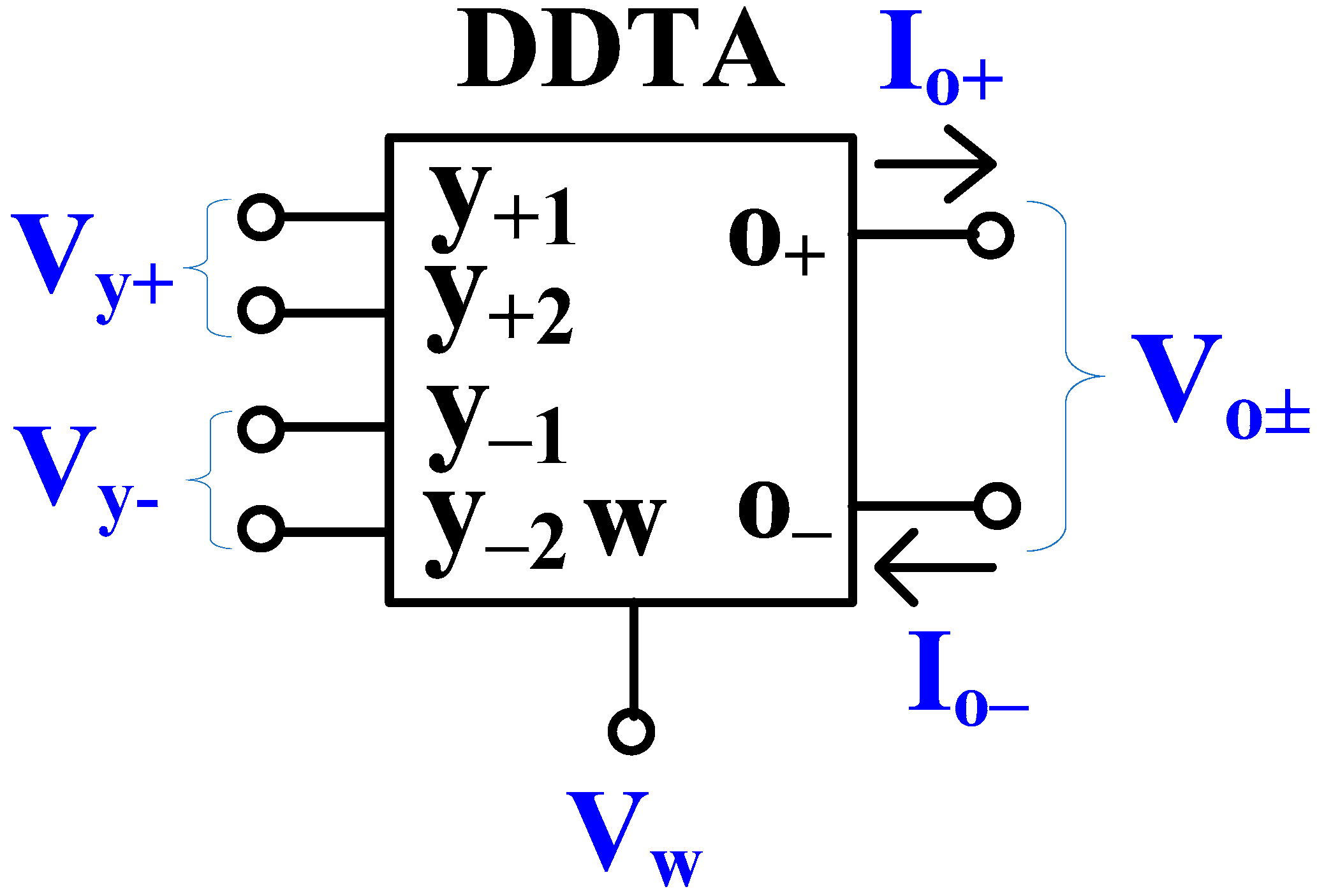
2. Proposed DDTA Circuit with Multiple-Input and Multiple-Output

The electrical symbol of the proposed multiple-input/output differential-difference transconductance amplifier is shown in Figure 1. Its performance, in an ideal case, is described by Equation (1). The circuit possesses one low-impedance output w, which provides a difference of the sums of the voltages Vy+ and Vy, applied to its non-inverting and inverting terminals, respectively. It further has a high-impedance output o, which provides a current, proportional to the voltage Vw appearing at the w terminal.
V w = V y + 1 + V y + 2 V y 1 V y 2 I o ± = ± g m V w
The CMOS structure of the proposed circuit is shown in Figure 2. The circuit consists of two blocks, a multiple-input differential-difference amplifier (MI-DDA) and a multiple-output transconductance amplifier (MO-TA).
The MI-DDA can be seen as a two-stage internal OTA, operating in a unity-gain feedback configuration. The first gain stage is formed by the transistors M1–M12, M14, M15, while the second stage is formed by the transistors M13 and M16. The capacitance CC is used for frequency compensation. The first stage can be seen as a current-mirror OTA, with a differential amplifier M1–M10 and a set of current mirrors M5–M12, M6–M11, M14–M15, acting as a differential to a single output converter.
The input stage is based on a non-tailed bulk-driven differential pair M1-M4, which behaves as a differential amplifier with high CMRR and PSRR performances, while also being able to operate at extremely low supply voltages [69], even lower than the threshold voltages of the used MOS transistors. In order to increase the voltage gain, a partial positive feedback (PPF) is applied. The PPF is created by two cross-coupled transistor pairs: M7–M8 and M9–M10. The cross-coupled pairs generate negative conductances that partially compensate for the conductances of the diode-connected transistors M2A,B for the “upper” pair, and M5, M6 for the “lower” pair. Therefore, the resulting conductances increase at the drains of these transistors, and, consequently, the first stage transconductance and voltage gain also increase. In particular, the upper pair increases the voltage gain from the bulk terminals to the gates of M1A,B [70], while the lower pair increases the current gains of the current mirrors M5–M12 and M6–M11 [71]. The combination of two PPF circuits decreases the overall sensitivity of the transconductance gain of the first stage to transistor mismatch [63]. This achieves a larger voltage gain while maintaining relatively low sensitivity of the input stage and avoiding problems with frequency compensation of the DDA.
In order to realize a differential to difference function without duplicating the input stage, the multiple inputs were realized using the so-called multiple-input BD MOS transistors [15]. The symbol and the implementation of the devices are shown in Figure 3a,b, respectively. A passive capacitive voltage divider is applied to the bulk terminal of the MOS transistor, thus creating a multiple-input device. The large resistors RMOSi, used to bias the bulk terminal for DC, are realized using two minimum-size MOS transistors operating in a cut-off region, as shown in Figure 3c.
Assuming 1/ωCBi << RMOSi, the voltage Vb at the bulk terminal of the MI-BD-MOS transistor can be expressed as:
V b = i = 1 n β i V i
where n is the number of inputs and βi is the voltage gain of the input capacitive divider:
β i = C B i i = 1 n C B i
Note that with equal CBi, βi = 1/n.
The open-loop voltage gain of the DDA can be expressed as:
A v o = β 2 g m b 1 r d s 15 | | r d s 12 g m 16 r d s 16 | | r d s 13 1 m 1 1 m 2
where the coefficients m1 and m2 are the ratios of the absolute values of the negative and positive conductances in a lower and upper PPF circuit, respectively [62]:
m 1 = g m 9,10 g m 5,6 + g d s 2 + g d s 3,4 + g d s 7,8 g m 9,10 g m 5,6
m 2 = g m 7,8 g m 2 + g d s 1 + g d s 5,6 + g d s 9,10 g m 7,8 g m 2
Note that the above coefficients should always be lower than unity to maintain circuit stability. In the proposed design, m1 = m2 = 0.5. This increased the voltage gain by 12 dB, thus compensating for the gain loss introduced by the input capacitive divider (approximately 10 dB) while maintaining the overall circuit sensitivity to transistor mismatch at a relatively low level.
The second block creating the MIMO-DDTA is the multiple output transconductance amplifier. The circuit can be seen as a current-mirror linear OTA. Note that a version of the MI-TA with one positive output was presented and verified experimentally in [18]. Here, a second, inverting output has been added, thus increasing the circuit universality. Transistors M1, M2 and M11, M12 realize an input differential stage. The transistors M11 and M12 operate in a triode region and extend the linear range of the structure. The circuit can be seen as a BD version of the Krummenacher and Joehl transconductor [72], operating in weak inversion. Thanks to the BD approach, the linear range of the circuit is extended η = gm1,2/gmb1,2 times, as compared with its gate-driven (GD) counterpart. In order to obtain optimum linearity, the following condition should be met [18]:
k = W / L 11,12 W / L 1,2 = 0.5
where W and L are the MOS transistor channel width and length, respectively.
Assuming unity current gain of all current mirrors, the circuit transconductance is given by:
g m = η 4 k 4 k + 1 · I s e t n p U T
where np is the subthreshold slope factor, UT is the thermal potential and Iset is the biasing current. Note that the circuit transconductance is proportional to this current.
In order to increase the DC voltage gain of the structure while not limiting its output voltage range, all current mirrors are based on self-cascode transistors. Consequently, the DC voltage gain from the input to the differential output is equal to:
A V O 2 g m [ g m 9 r d s 9 r d s 9 c | | g m 6 r d s 6 r d s 6 c ]
Thanks to the self-cascode technique, it is possible to compensate for the gain loss associated with the application of the BD technique. In practice, a voltage gain of around 40 dB can be obtained.

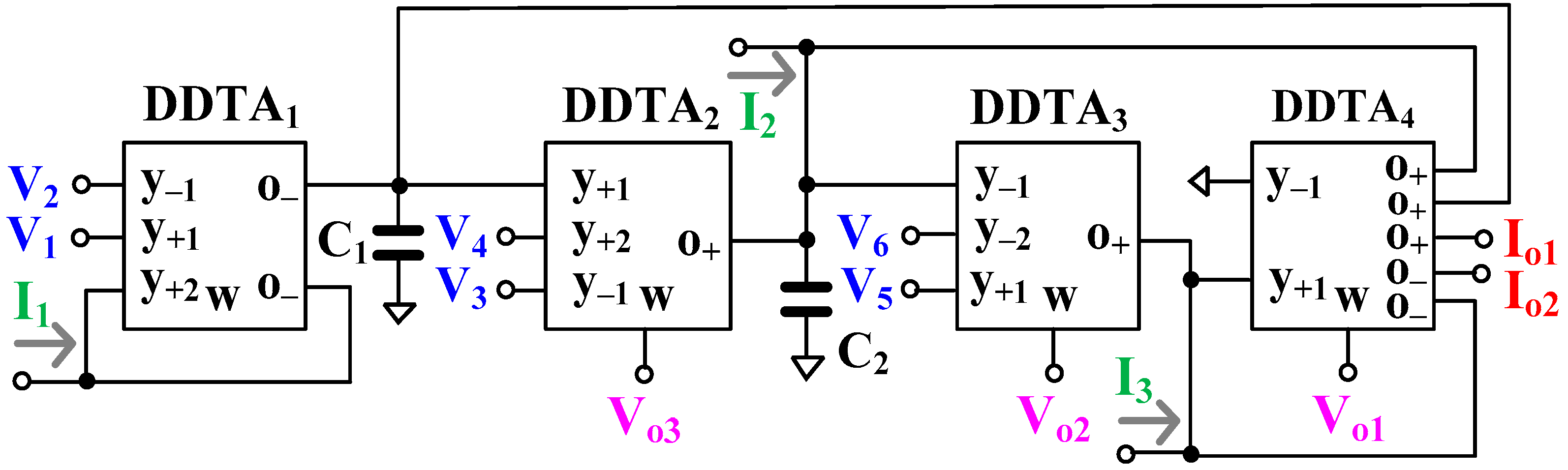
3. Versatile Mixed-Mode Filter

Figure 4 shows the proposed versatile mixed-mode universal filter employing four MIMO-DDTAs and two grounded capacitors. Using (1) and nodal analysis, the output voltages Vo1, Vo2, Vo3 and the output currents Io1, Io2 can be given by:
V o 1 = g m 3 g m 4 · s 2 C 1 C 2 V 5 V 6 + s C 1 g m 2 V 3 V 4 + g m 1 g m 2 V 1 V 2 s 2 C 1 C 2 + s C 1 g m 3 + g m 2 g m 3
V o 2 = s 2 C 1 C 2 V 5 V 6 + s C 1 g m 2 V 3 V 4 + g m 1 g m 2 V 1 V 2 s 2 C 1 C 2 + s C 1 g m 3 + g m 2 g m 3
V o 3 = s C 2 g m 3 V 5 V 6 + s 2 C 1 C 2 + s C 2 g m 3 V 3 V 4 + s C 2 g m 3 + g m 1 g m 3 V 1 V 2 s 2 C 1 C 2 + s C 1 g m 3 + g m 2 g m 3
I o 1 = g m 3 · s 2 C 1 C 2 V 5 V 6 + s C 1 g m 2 V 3 V 4 + g m 1 g m 2 V 1 V 2 s 2 C 1 C 2 + s C 1 g m 3 + g m 2 g m 3
I o 1 = s 2 C 1 C 2 I 3 + s C 1 g m 3 I 2 g m 2 g m 3 I 1 s 2 C 1 C 2 + s C 1 g m 3 + g m 2 g m 3
I o 2 = s 2 C 1 C 2 I 3 s C 1 g m 3 I 2 + g m 2 g m 3 I 1 s 2 C 1 C 2 + s C 1 g m 3 + g m 2 g m 3
V o 1 = 1 g m 4 · s 2 C 1 C 2 I 3 + s C 1 g m 3 I 2 g m 2 g m 3 I 1 s 2 C 1 C 2 + s C 1 g m 3 + g m 2 g m 3
From (10)–(16), the variant filtering functions can be determined and are shown in Table 1. The proposed mixed-mode universal filter can offer LP, HP, BP, BS, and AP filtering functions of VM, CM, TAM, and TIM in the same topology. Thanks to the multiple inputs of the DDTA, the VM, CM, and TIM can offer non-inverting and inverting transfer functions of LP, HP, BP, BS, and AP filters, and the VM and TAM can also offer differential transfer functions of LP, HP, BP, BS, and AP filters. Thus, the proposed mixed-mode filter can provide 61 transfer functions in a single topology. Thanks to the multiple outputs of the DDTA, such as DDTA4, the proposed filter utilizes a minimum number of used DDTAs while offering inverting and non-inverting transfer functions of LP, HP, BP, BS, and AP filters of CM. The input signals V1 to V6 are connected to the high-impedance terminals of the DDTA; thus, the voltage signals can be applied without any buffer circuit requirements. The output signals Vo1 to Vo3 are connected to the low-impedance terminals of the DDTA, which offers a cascadable output for the voltage-mode filter structures. The output signals Io1 and Io2 are connected to the high-impedance terminals of the DDTA, which offers a cascadable output for the current-mode filter structures. However, in the case of CM, the inputs I1 to I3 require additional circuits, such as multiple-output current followers or multiple-output current mirrors, to create three identical current signals from the single original current signal. It is clear that the proposed filter is exempt from inverting-type input signal and input matching conditions for realizing all filtering functions both in the case of voltage and current signals.
The voltage gain gm3/gm4 of the filtering functions can be obtained if the output Vo1 is used. In the case of TAM, the inputs V1 to V6 are converted to output currents by gm3; in the case of TIM, the input currents I1 to I3 are converted to output voltages by gm4.
The natural frequency (ωo) and the quality factor (Q) can be given by:
ω o = g m 2 g m 3 C 1 C 2
Q = C 2 g m 2 C 1 g m 3
It should be noted that the parameter ωo can be controlled electronically by gm2 and gm3 and the parameter Q can be given by C2/C1.

Non-Ideality Analysis

Taking the tracking errors and the non-ideal transconductance of the MIMO-DDTA into account, the characteristics of the MIMO-DDTA can be rewritten as:
V w = α j + V y + 1 + α j + V y + 2 α j V y + α j V y 2 I o = g m n j V w
where αj+ =1–εj+v and εj+v (|εj+v |≪ 1) denote the voltage tracking error from non-inverting terminals (i.e., Vy+1, Vy+2) to the w-terminal (i.e., Vw) of the j-th DDTA, αj =1–εj-v and εj-v (|εj-v|≪ 1) denote the voltage tracking error from inverting terminals (i.e., Vy−1, Vy−2) to the w-terminal (i.e., Vw) of the j-th DDTA, and gmnj is the non-ideal transconductance gain of the j-th DDTA. The non-ideal transconductance gmnj of the j-th DDTA at a frequency near the cut-off frequency can be expressed by [59]:
g m n j s g m j 1 μ j s
where μj= 1⁄ωgmj, ωgmj denotes the first pole frequency of the j-th gm.
Using (19), the denominator of (10)–(16) can be modified as:
s 2 C 1 C 2 + s C 1 g m n 3 α 3 + g m n 2 g m n 3 α 2 + α 3
Using (20), (21) becomes:
s 2 C 1 C 2 1 C 1 g m 3 μ 3 α 3 g m 2 g m 3 α 2 + α 3 μ 2 μ 3 C 1 C 2 + s C 1 g m 3 α 3 1 g m 2 g m 3 α 2 + α 3 μ 2 + μ 3 C 1 g m 3 α 3 + g m 2 g m 3 α 2 + α 3
The tracking errors and the non-ideal effect of the transconductance of the DDTA can be made negligible by satisfying the following condition:
g m 2 g m 3 α 2 + α 3 μ 2 + μ 3 C 1 g m 3 α 3 1 C 1 g m 3 μ 3 α 3 g m 2 g m 3 α 2 + α 3 μ 2 μ 3 C 1 C 2 1
The modified natural frequency (ωon) and the modified quality factor (Qn) can be expressed as:
ω o n = g m 2 g m 3 C 1 C 2 · α 2 + α 3
Q n = C 2 g m 2 C 1 g m 3 · α 2 + α 3
To consider the parasitic impedances that affect the proposed mixed-mode filter, the parasitic capacitance Co and parasitic conductance go (go = 1/Ro, Ro is the output resistance) at the o-terminal of the DDTA are considered while the parasitic impedances at the y- and w-terminals are neglected. Considering Figure 4, the parasitic capacitances Co1, Co4 and parasitic conductances go1, go4 are parallel with C1 and the parasitic capacitances Co2, Co4, and parasitic conductances go2, go4 are parallel with C2. Co1, Co2, Co4 are, respectively, the parasitic capacitances at the o-terminal of DDTA1, DDTA2, DDTA4, and go1, go2, go4 are, respectively, the parasitic conductances at the o-terminal of DDTA1, DDTA2, DDTA4. The parasitic capacitances can be neglected by appropriately choosing values such that C1Co4 + Co4, C2Co2 + Co4, gm2go1 + go4, and gm3go2 + go4.

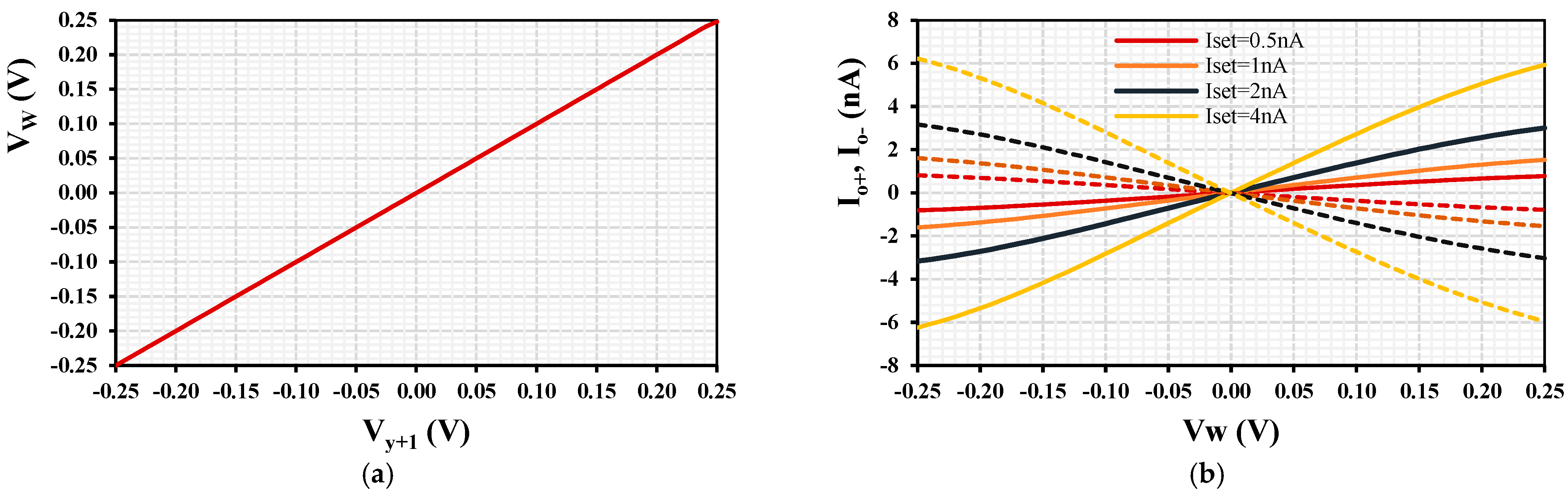
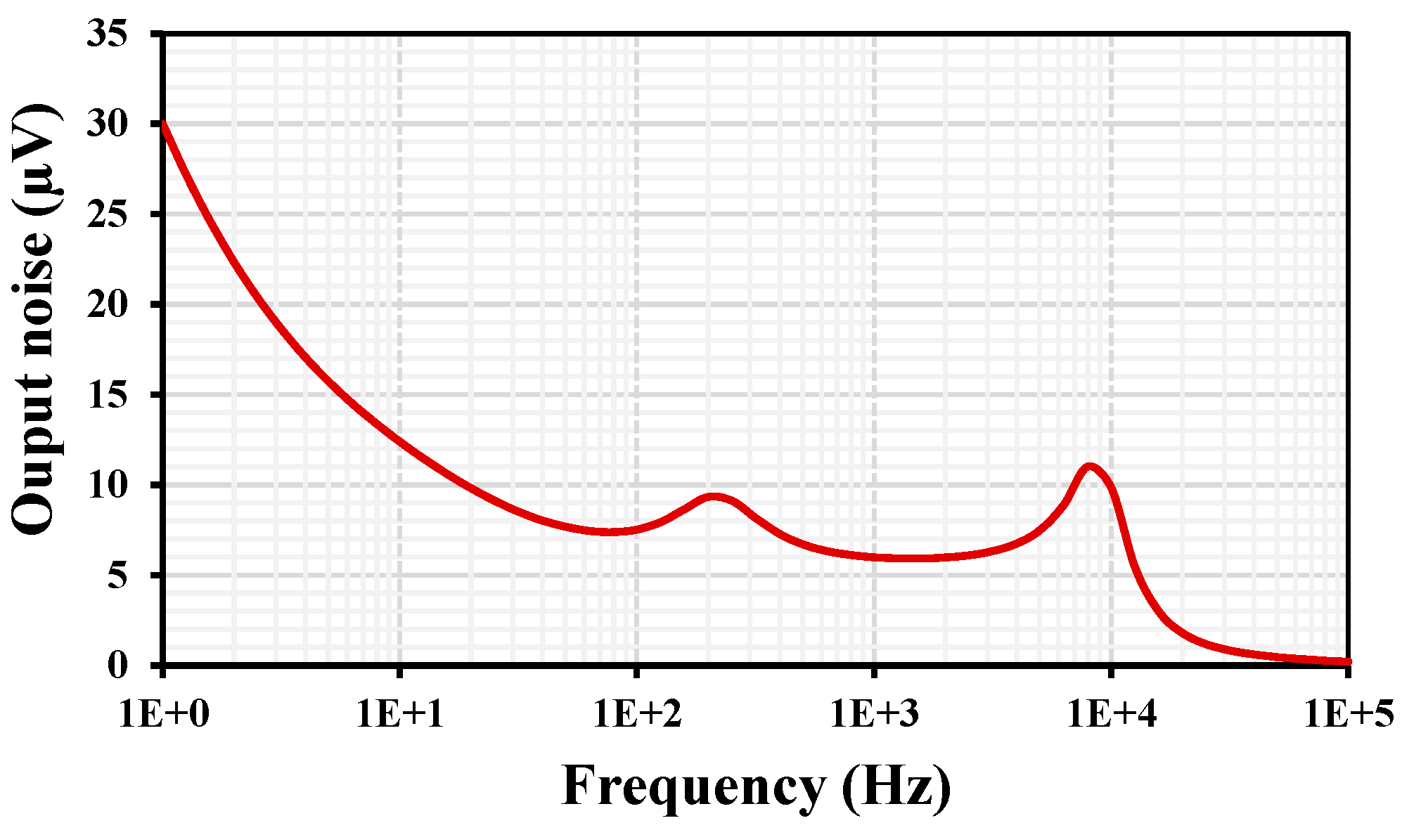
4. Simulation Results

The circuit was designed and simulated using the Cadence Virtuoso System Design Platform using 0.18 µm CMOS technology from TSMC. The voltage supply was ±250 mV (0.5 V) and the bias voltage VB1 = −100 mV. The transistor aspect ratios are included in Table 2. It is worth noting that the only increase in chip area is due to the input capacitor CB = 0.5 pF, so the total input capacitance of the proposed MIMO-DDTA is 3 pF. This value is acceptable for integration.
Selected simulation results for the MIMO-DDTA are shown in Figure 5 and Figure 6. Figure 5 shows the simulated results of the DC transfer characteristic of the MI-DDA Vw versus Vy+1 and of the MO-TA Io+, Io versus Vw with various Iset. The extended linearity of operation despite the low supply voltage is observed.
Figure 6 shows the impedances frequency characteristics of the MIMO-DDTA with Iset = 4 nA: (a) Zy, Zo+, Zo− and (b) ZW. At low frequency, the impedance of Zy = 29.5 GΩ, Zo+ =Zo− = 2.1 GΩ and Zw = 876 Ω. All these values are suitable for the proposed filter application.
For the filter application, for cutoff frequency 220 Hz and for Iset = 4 nA (gm = 27.7 nS) the Equation (17) has been used to calculate the value of capacitors C1 = C2 = 20 pF. The frequency responses of the gain and phase for the differential input VM, non-inverting CM, TAM and TIM filter with Iset1–4 = 4 nA are shown in Figure 7. The simulated cutoff frequency was 211 Hz, which is closed to the calculated one. This slight deviation in the cutoff frequency can be easily corrected by adjusting the setting current. The power consumption of the filter was 281 nW.
The frequency responses of LP, HP, BP, BS, and AP gains and phases for VM are shown in Figure 8. The wide tunability of the filter is achieved by varying the setting current Iset1–4 = (0.5, 1, 2, 4) nA, where the cutoff frequency was (28, 56, 112, 211) Hz, respectively.
Monte Carlo (MC) analysis was used to perform the statistical analysis to estimate the parametric yield and generate information about the performance characteristics of the differential input VM filter. The gains frequency responses of LP, HP, BP, BS, and AP with 200 runs MC are shown in Figure 9. The curves are overlapping or close to each other.
The process, voltage, and temperature (PVT) corners were also used to confirm the robustness of the design. The process transistor corners were fast–fast, fast–slow, slow–fast, and slow–slow. The process MIM capacitor corners were fast–fast and slow–slow. The voltage supply corners were = ±10% (VDD-VSS) and the temperature corners were −20 °C and 70 °C. The results for the gains frequency responses of LP, HP, BP, BS, and AP with PVT are shown in Figure 10. The curves are again overlapping or close to each other, which confirms the robustness of the filter design. In addition, thanks to the tunability of the filter, any deviation in the cutoff frequency can be easily adjusted by the setting current.
The transient response of the VM LPF with an applied input sinusoidal signal Vin-pp = 200 mV@10 Hz is shown in Figure 11a. The spectrum of the output signal is shown in Figure 11b, where the total harmonic distortion (THD) of 0.23% is indicated.
The THD for the VM LPF with different peak-to-peak input signal values @ 10 Hz is shown in Figure 12. The 1% THD is achieved for Vin-pp = 300 mV. The output voltage noise for the VM LPF is shown in Figure 13. The root-mean-square (RMS) output noise integrated in the bandwidth of 1 to 211 Hz was 130 μV; thus, the dynamic range (DR) of the VM LPF filter is 58.23 dB @ 1% THD.
The proposed versatile mixed-mode filter was compared with the previously reported filters in [29,32,45,51,59,60,61] as shown in Table 3. Compared with these previous works, the proposed filter offers the most transfer functions of the five standard filtering functions and the lowest voltage supply. Compared with [29,32], the proposed filter offers electronic tuning capability of the natural frequency; compared with [59,60,61], the proposed filter uses fewer active devices. The filters in [32,45,51] apply the input signal via capacitor and/or resistor, the structure in [45] does not provide five standard filtering functions of VM, CM, TAM, and TIM, and the filters in [45,51] require input matching conditions for realizing some filtering functions.

5. Conclusions

This paper presents a 0.5 V, 281 nW versatile mixed-mode universal filter using MIMO-DDTAs. The MIMO-DDTA is used to realize a versatile mixed-mode universal filter that offers many transfer functions in the same topology. To realize variant transfer functions such as LPF, HPF, BPF, BSF, and APF of VM, CM, TAM, and TIM, inverted input signal requirement is absent. The natural frequency can be electronically controlled. The VM filter offers high-input impedance and low-output impedance, and the CM filter offers high-output impedance. For the VM LP filter, the dynamic range was 58.23 dB @ 1% total harmonic distortion. The proposed filter was designed and simulated in the Cadence Virtuoso System Design Platform using the 0.18 µm CMOS technology from TSMC. The simulation results, including Monte-Carlo and PVT corners, confirm the functionality of the design.

Author Contributions

Conceptualization, F.K., M.K. and T.K.; methodology, M.K. and F.K.; software, F.K.; validation, F.K. and T.K.; formal analysis, T.K., M.K. and F.K., investigation, F.K. and M.K.; resources, F.K. and M.K.; writing—original draft preparation, M.K., F.K. and T.K.; writing—review and editing, F.K. and T.K.; visualization, F.K., T.K. and M.K.; supervision, F.K.; project administration, F.K.; funding acquisition, F.K. and M.K. All authors have read and agreed to the published version of the manuscript.

Funding

This work was supported by the University of Defence within the Organization Development Project VAROPS.

Institutional Review Board Statement

Not applicable.

Informed Consent Statement

Not applicable.

Data Availability Statement

Data are contained within the article.

Conflicts of Interest

The authors declare no conflict of interest.

References

  1. Wyszynski, A.; Schaumann, R. Using multiple-input transconductors to reduce number of components in OTA-C filter design. Electron. Lett. 1992, 28, 217–220. [Google Scholar] [CrossRef]
  2. Chiang, D.H.; Schaumann, R. A CMOS fully-balanced continuous-time IFLF filter design for read/write channels. In Proceedings of the 1996 IEEE International Symposium on Circuits and Systems, Circuits and Systems Connecting the World, ISCAS 96, Atlanta, GA, USA, 15 May 1996; Volume 1, pp. 167–170. [Google Scholar] [CrossRef]
  3. Gopinathan, V.; Tsividis, Y.P.; Tan, K.S.; Hester, R.K. Design considerations for high-frequency continuous-time filters and implementation of an antialiasing filter for digital video. IEEE J. Solid State Circuits 1990, 25, 1368–1378. [Google Scholar] [CrossRef]
  4. Glinianowicz, J.; Jakusz, J.; Szczepanski, S.; Sun, Y. High-frequency two-input CMOS OTA for continuous-time filter applications. IEEE Proc. Circuits Devices Syst. 2000, 147, 13. [Google Scholar] [CrossRef]
  5. Sackinger, E.; Guggenbuhl, W. A versatile building block: The CMOS differential difference amplifier. IEEE J. Solid State Circuits 1987, 22, 287–294. [Google Scholar] [CrossRef]
  6. Huang, S.C.; Ismail, M.; Zarabadi, S.R. A wide range differential difference amplifier: A basic block for analog signal processing in MOS technology. IEEE Trans. Circuits Syst. II Analog. Digit. Signal Process. 1993, 40, 289–301. [Google Scholar] [CrossRef]
  7. Zarabadi, S.R.; Larsen, F.; Ismail, M. A reconfigurable op-amp/DDA CMOS amplifier architecture. IEEE Trans. Circuits Syst. I Fundam. Theory Appl. 1992, 39, 484–487. [Google Scholar] [CrossRef]
  8. Czarnul, Z.; Takagi, S.; Fujii, N. Common-mode feedback circuit with differential-difference amplifier. IEEE Trans. Circuits Syst. I Fundam. Theory Appl. 1994, 41, 243–246. [Google Scholar] [CrossRef]
  9. Duque-Carrillo, J.F.; Torelli, G.; Perez-Aloe, R.; Valverde, J.M.; Maloberti, F. Fully differential basic building blocks based on fully differential difference amplifiers with unity-gain difference feedback. IEEE Trans. Circuits Syst. I Fundam. Theory Appl. 1995, 42, 190–192. [Google Scholar] [CrossRef]
  10. Chiu, W.; Liu, S.I.; Tsao, H.W.; Chen, J.J. CMOS differential difference current conveyors and their applications. IEEE Proc. Circuits Devices Syst. 1996, 143, 91–96. [Google Scholar] [CrossRef]
  11. Elwan, H.O.; Soliman, A.M. Novel CMOS differential voltage current conveyor and its applications. IEEE Proc. Circuits Devices Syst. 1997, 144, 195–200. [Google Scholar] [CrossRef]
  12. Mahmoud, S.A.; Soliman, A.M. The differential difference operational floating amplifier: A new block for analog signal processing in MOS technology. IEEE Trans. Circuits Syst. II Analog. Digit. Signal Process. 1998, 45, 148–158. [Google Scholar] [CrossRef]
  13. Kumngern, M. CMOS differential difference voltage follower transconductance amplifier. In Proceedings of the 2015 IEEE International Circuits and Systems Symposium (ICSyS), Langkawi, Malaysia, 2–4 September 2015; pp. 133–136. [Google Scholar] [CrossRef]
  14. Rana, P.; Ranjan, A. Odd- and even-order electronically controlled wave active filter employing differential difference trans-conductance amplifier (DDTA). Int. J. Electron. 2021, 108, 1623–1651. [Google Scholar] [CrossRef]
  15. Khateb, F.; Kulej, T.; Kumngern, M.; Psychalinos, C. Multiple-Input Bulk-Driven MOS Transistor for Low-Voltage Low-Frequency Applications. Circuits Syst. Signal Process. 2019, 38, 2829–2845. [Google Scholar] [CrossRef]
  16. Khateb, F.; Kulej, T.; Veldandi, H.; Jaikla, W. Multiple-input bulk-driven quasi-floating-gate MOS transistor for low-voltage low-power integrated circuits. AEU Int. J. Electron. Commun. 2019, 100, 32–38. [Google Scholar] [CrossRef]
  17. Khateb, F.; Kulej, T.; Kumngern, M.; Jaikla, W.; Ranjan, R.K. Comparative performance study of multiple-input bulk-driven and multiple-input bulk-driven quasi-floating-gate DDCCs. AEU Int. J. Electron. Commun. 2019, 108, 19–28. [Google Scholar] [CrossRef]
  18. Khateb, F.; Kulej, T.; Akbari, M.; Tang, K.T. A 0.5-V Multiple-Input Bulk-Driven OTA in 0.18-μm CMOS. IEEE Trans. Very Large Scale Integr. Syst. 2022, 30, 1739–1747. [Google Scholar] [CrossRef]
  19. Khateb, F.; Kumngern, M.; Kulej, T.; Akbari, M.; Stopjakova, V. 0.5 V, nW-Range Universal Filter Based on Multiple-Input Transconductor for Biosignals Processing. Sensors 2022, 22, 8619. [Google Scholar] [CrossRef]
  20. Khateb, F.; Kumngern, M.; Kulej, T.; Yavari, M. 0.5-V Nano-Power Shadow Sinusoidal Oscillator Using Bulk-Driven Multiple-Input Operational Transconductance Amplifier. Sensors 2023, 23, 2146. [Google Scholar] [CrossRef]
  21. Khateb, F.; Kumngern, M.; Kulej, T. 0.5-V Nano-Power Voltage-Mode First-Order Universal Filter Based on Multiple-Input OTA. IEEE Access 2023, 11, 49806–49818. [Google Scholar] [CrossRef]
  22. Kumngern, M.; Khateb, F.; Kulej, T. Extremely low-voltage low-power differential difference current conveyor using multiple-input bulk-driven technique. AEU Int. J. Electron. Commun. 2020, 123, 153310. [Google Scholar] [CrossRef]
  23. Kumngern, M.; Khateb, F.; Kulej, T. 0.3 V Differential Difference Current Conveyor Using Multiple-Input Bulk-Driven Technique. Circuits Syst. Signal Process. 2020, 39, 3189–3205. [Google Scholar] [CrossRef]
  24. Khateb, F.; Kumngern, M.; Kulej, T.; Psychalinos, C. 0.5 V Universal Filter Based on Multiple-Input FDDAs. Circuits Syst. Signal Process. 2019, 38, 5896–5907. [Google Scholar] [CrossRef]
  25. Abuelma’Atti, M.T.; Bentrcia, A.; Al-Shahrani, S.M. A novel mixed-mode current-conveyor-based filter. Int. J. Electron. 2004, 91, 191–197. [Google Scholar] [CrossRef]
  26. Abuelma’Atti, M.T.; Bentrcia, A. A Novel Mixed-Mode CCII-Based Filter. Act. Passiv. Electron. Components 2004, 27, 197–205. [Google Scholar] [CrossRef]
  27. Lee, C.-N.; Chang, C.-M. Single FDCCII-based mixed-mode biquad filter with eight outputs. AEU Int. J. Electron. Commun. 2008, 63, 736–742. [Google Scholar] [CrossRef]
  28. Minaei, S.; Ibrahim, M.A. A mixed-mode KHN-biquad using DVCC and grounded passive elements suitable for direct cascading. Int. J. Circuit Theory Appl. 2008, 37, 793–810. [Google Scholar] [CrossRef]
  29. Lee, C.-N. Fully Cascadable Mixed-Mode Universal Filter Biquad Using DDCCs and Grounded Passive Components. J. Circuits Syst. Comput. 2011, 20, 607–620. [Google Scholar] [CrossRef]
  30. Liao, W.B.; Gu, J.C. SIMO type universal mixed-mode biquadratic filter. Indian J. Eng. Mater. Sci. 2011, 18, 443–448. [Google Scholar]
  31. Ghosh, K.; Ray, B.N. CCII-Based Nth-Order Mixed Mode Elliptic Filter with Grounded R and C. J. Circuits Syst. Comput. 2015, 24, 1550035. [Google Scholar] [CrossRef]
  32. Lee, C.-N. Independently tunable mixed-mode universal biquad filter with versatile input/output functions. AEU Int. J. Electron. Commun. 2016, 70, 1006–1019. [Google Scholar] [CrossRef]
  33. Lee, C.-N. Mixed-Mode Universal Biquadratic Filter with No Need of Matching Conditions. J. Circuits Syst. Comput. 2016, 25, 1650106. [Google Scholar] [CrossRef]
  34. Tsukutani, T.; Kinugasa, Y.; Yabuki, N. A novel mixed-mode universal biquad employing plus current output DVCCs. Adv. Sci. Technol. Eng. Syst. J. 2018, 3, 236–240. [Google Scholar] [CrossRef]
  35. Singh, V.K.; Singh, A.K.; Bhaskar, D.R.; Senani, R. Novel mixed-mode universal biquad configuration. IEICE Electron. Express 2005, 2, 548–553. [Google Scholar] [CrossRef]
  36. Pandey, N.; Paul, S.K.; Bhattacharyya, A.; Jain, S.B. A new mixed mode biquad using reduced number of active and passive elements. IEICE Electron. Express 2006, 3, 115–121. [Google Scholar] [CrossRef]
  37. Yuce, E. Fully integrable mixed-mode universal biquad with specific application of the CFOA. AEU Int. J. Electron. Commun. 2010, 64, 304–309. [Google Scholar] [CrossRef]
  38. Shah, N.A.; Malik, M.A. Multifunction mixed-mode filter using FTFNs. Analog. Integr. Circuits Signal Process. 2006, 47, 339–343. [Google Scholar] [CrossRef]
  39. Abuelma’Atti, M.T. A Novel Mixed-Mode Current-Controlled Current-Conveyor-Based Filter. Act. Passiv. Electron. Components 2003, 26, 185–191. [Google Scholar] [CrossRef]
  40. Zhijun, L. Mixed-mode universal filter using MCCCII. AEU Int. J. Electron. Commun. 2009, 63, 1072–1075. [Google Scholar] [CrossRef]
  41. Pandey, N.; Paul, S.K. Mixed Mode Universal Filter. J. Circuits Syst. Comput. 2013, 22, 1250064. [Google Scholar] [CrossRef]
  42. Agrawal, D.; Maheshwari, S. High-Performance Electronically Tunable Analog Filter Using a Single EX-CCCII. Circuits Syst. Signal Process. 2021, 40, 1127–1151. [Google Scholar] [CrossRef]
  43. Maheshwari, S.; Singh, S.V.; Chauhan, D.S. Electronically tunable low-voltage mixed-mode universal biquad filter. IET Circuits Devices Syst. 2011, 5, 149–158. [Google Scholar] [CrossRef]
  44. Faseehuddin, M.; Albrni, M.A.; Herencsar, N.; Sampe, J.; Ali, S.H.M. Novel Electronically Tunable Biquadratic Mixed- Mode Universal Filter Capable of Operating in MISO and SIMO Configurations. Inf. MIDEM 2020, 50, 189–204. [Google Scholar] [CrossRef]
  45. Singh, S.V.; Tomar, R.S.; Goswami, M. A Current Tunable Mixed Mode ZC-CCTAs Based Resistor Less Universal Filter. J. Circuits Syst. Comput. 2021, 30, 2150225. [Google Scholar] [CrossRef]
  46. Chen, H.-P.; Yang, W.S. Electronically Tunable Current Controlled Current Conveyor Transconductance Amplifier-Based Mixed-Mode Biquadratic Filter with Resistorless and Grounded Capacitors. Appl. Sci. 2017, 7, 244. [Google Scholar] [CrossRef]
  47. Yesil, A.; Kacar, F. Electronically tunable resistorless mixed-mode biquad filters. Radioengineering 2013, 22, 1016–1125. [Google Scholar]
  48. Faseehuddin, M.; Herencsar, N.; Albrni, M.A.; Shireen, S.; Sampe, J. Electronically tunable mixed mode universal filter employing grounded capacitors utilizing highly versatile VD-DVCC. Circuit World 2022, 48, 511–528. [Google Scholar] [CrossRef]
  49. Mishra, R.; Mishra, G.R.; Mishra, S.O.; Faseehuddin, M. Electronically Tunable Mixed Mode Universal Filter Employing Grounded Passive Components. Inf. MIDEM J. Microelectron. Electron. Components Mater. 2022, 52, 105–115. [Google Scholar] [CrossRef]
  50. Roongmuanpha, N.; Faseehuddin, M.; Herencsar, N.; Tangsrirat, W. Tunable Mixed-Mode Voltage Differencing Buffered Amplifier-Based Universal Filter with Independently High-Q Factor Controllability. Appl. Sci. 2021, 11, 9606. [Google Scholar] [CrossRef]
  51. Faseehuddin, M.; Herencsar, N.; Shireen, S.; Tangsrirat, W.; Ali, S.H.M. Voltage Differencing Buffered Amplifier-Based Novel Truly Mixed-Mode Biquadratic Universal Filter with Versatile Input/Output Features. Appl. Sci. 2022, 12, 1229. [Google Scholar] [CrossRef]
  52. Abuelma’Atti, M.T.; Bentrcia, A. A novel mixed-mode OTA-C universal filter. Int. J. Electron. 2005, 92, 375–383. [Google Scholar] [CrossRef]
  53. Bhaskar, D.R.; Singh, A.K.; Sharma, R.K.; Senani, R. New OTA-C universal current-mode/trans-admittance biquads. IEICE Electron. Express 2005, 2, 8–13. [Google Scholar] [CrossRef]
  54. Chen, H.-P.; Liao, Y.-Z.; Lee, W.-T. Tunable mixed-mode OTA-C universal filter. Analog. Integr. Circuits Signal Process. 2008, 58, 135–141. [Google Scholar] [CrossRef]
  55. Lee, C.-N. Multiple-Mode OTA-C Universal Biquad Filters. Circuits Syst. Signal Process. 2009, 29, 263–274. [Google Scholar] [CrossRef]
  56. Zanjani, S.M.A.; Dousti, M.; Dolatshahi, M. Inverter-based, low-power and low-voltage, new mixed-mode Gm-C filter in subthreshold CNTFET technology. IET Circuits Devices Syst. 2018, 12, 681–688. [Google Scholar] [CrossRef]
  57. Parvizi, M.; Taghizadeh, A.; Mahmoodian, H.; Kozehkanani, Z.D. A Low-Power Mixed-Mode SIMO Universal Gm–C Filter. J. Circuits Syst. Comput. 2017, 26, 1750164. [Google Scholar] [CrossRef]
  58. Parvizi, M. Design of a new low power MISO multi-mode universal biquad OTA-C filter. Int. J. Electron. 2019, 106, 440–454. [Google Scholar] [CrossRef]
  59. Bhaskar, D.R.; Raj, A.; Kumar, P. Mixed-Mode Universal Biquad Filter Using OTAs. J. Circuits Syst. Comput. 2020, 29, 2050162. [Google Scholar] [CrossRef]
  60. Namdari, A.; Dolatshahi, M. Design of a low-voltage and low-power, reconfigurable universal OTA-C filter. Analog. Integr. Circuits Signal Process. 2022, 111, 169–188. [Google Scholar] [CrossRef]
  61. Kumngern, M.; Suksaibul, P.; Khateb, F.; Kulej, T. 1.2 V Differential Difference Transconductance Amplifier and Its Application in Mixed-Mode Universal Filter. Sensors 2022, 22, 3535. [Google Scholar] [CrossRef]
  62. Kumngern, M.; Khateb, F.; Kulej, T. 0.5 V Universal Filter and Quadrature Oscillator Based on Multiple-Input DDTA. IEEE Access 2023, 11, 9957–9966. [Google Scholar] [CrossRef]
  63. Khateb, F.; Kumngern, M.; Kulej, T.; Biolek, D. 0.5 V Differential Difference Transconductance Amplifier and Its Application in Voltage-Mode Universal Filter. IEEE Access 2022, 10, 43209–43220. [Google Scholar] [CrossRef]
  64. Khateb, F.; Kumngern, M.; Kulej, T.; Biolek, D. 0.3-Volt Rail-to-Rail DDTA and Its Application in a Universal Filter and Quadrature Oscillator. Sensors 2022, 22, 2655. [Google Scholar] [CrossRef] [PubMed]
  65. Kulej, T.; Kumngern, M.; Khateb, F.; Arbet, D. 0.5 V Versatile Voltage- and Transconductance-Mode Analog Filter Using Differential Difference Transconductance Amplifier. Sensors 2023, 23, 688. [Google Scholar] [CrossRef] [PubMed]
  66. Khateb, F.; Kumngern, M.; Kulej, T.; Ranjan, R.K. 0.5 V Multiple-Input Multiple-Output Differential Difference Transconductance Amplifier and Its Applications to Shadow Filter and Oscillator. IEEE Access 2023, 11, 31212–31227. [Google Scholar] [CrossRef]
  67. Kumngern, M.; Khateb, F.; Kulej, T.; Steffan, P. 0.3-V Voltage-Mode Versatile First-Order Analog Filter Using Multiple-Input DDTAs. Sensors 2023, 23, 5945. [Google Scholar] [CrossRef]
  68. Kumngern, M.; Suksaibul, P.; Khateb, F.; Kulej, T. Electronically Tunable Universal Filter and Quadrature Oscillator Using Low-Voltage Differential Difference Transconductance Amplifiers. IEEE Access 2022, 10, 68965–68980. [Google Scholar] [CrossRef]
  69. Kulej, T. 0.5-V bulk-driven CMOS operational amplifier. IET Circuits Devices Syst. 2013, 7, 352–360. [Google Scholar] [CrossRef]
  70. Kulej, T. 0.4-V Bulk-Driven Operational Amplifier with Improved Input Stage. Circuits Syst. Signal Process. 2015, 34, 1167–1185. [Google Scholar] [CrossRef]
  71. Kulej, T.; Khateb, F. 0.4-V bulk-driven differential-difference amplifier. Microelectron. J. 2015, 46, 362–369. [Google Scholar] [CrossRef]
  72. Krummenacher, F.; Joehl, N. A 4-MHz CMOS continuous-time filter with on-chip automatic tuning. IEEE J. Solid State Circuits 1988, 23, 750–758. [Google Scholar] [CrossRef]
Figure 1. Electrical symbol of the MIMO-DDTA.
Sensors 24 00032 g001
Figure 2. CMOS structure of the MIMO-DDTA.
Sensors 24 00032 g002
Figure 3. MI-BD MOST: (a) symbol, (b) possible implementation, (c) implementation of RMOS.
Sensors 24 00032 g003
Figure 4. The proposed versatile mixed-mode filter using MIMO-DDTAs.
Sensors 24 00032 g004
Figure 5. The DC transfer characteristics of the MIMO-DDTA: (a) Vw versus Vy+1 and (b) Io+, Io (dashed line) versus Vw with various Iset.
Sensors 24 00032 g005
Figure 6. The impedances frequency characteristics of the MIMO-DDTA: (a) Zy, Zo+, Zo− and (b) ZW.
Sensors 24 00032 g006
Figure 7. The frequency characteristics of gains for the VM (a), CM (b), TAM (c), and TIM (d).
Sensors 24 00032 g007
Figure 8. The frequency characteristics of gains (lines) and phases (points) for the VM filter: LPF (a), HPF (b), BPF (c), BSF (d), and APF (e).
Sensors 24 00032 g008
Figure 9. The 200 runs MC frequency characteristics of the gains for the differential input VM filter: LPF (a), HPF (b), BPF (c), BSF (d), and APF (e).
Sensors 24 00032 g009
Figure 10. The PVT frequency characteristics of the gains for the VM filter: LPF (a), HPF (b), BPF (c), BSF (d), and APF (e).
Sensors 24 00032 g010
Figure 11. The transient response of the VM LPF (a) and the spectrum of the output signal (b).
Sensors 24 00032 g011
Figure 12. The THD of the VM LPF with different peak-to-peak input voltages @ 10 Hz.
Sensors 24 00032 g012
Figure 13. The output voltage noise of the VM LPF.
Sensors 24 00032 g013
Table 1. Obtaining variant filtering functions of the proposed versatile mixed-mode filter.
Operation ModeFiltering FunctionInputOutput
VMLPNon-inverting V 1 V o 1
Inverting V 2 V o 1
Non-inverting V 1 V o 2
Inverting V 2 V o 2
Non-inverting V 1 = V 6 V o 3
Inverting V 2 = V 5 V o 3
Differential V 1 V 2 V o 2
BPNon-inverting V 3 V o 1
Inverting V 4 V o 1
Non-inverting V 3 V o 2
Inverting V 4 V o 2
Non-inverting V 5 V o 3
Inverting V 6 V o 3
Differential V 3 V 4 V o 2
HPNon-inverting V 5 V o 1
Inverting V 6 V o 1
Non-inverting V 5 V o 2
Inverting V 6 V o 2
Non-inverting V 3 = V 6 V o 3
Inverting V 4 = V 5 V o 3
Differential V 5 V 6 V o 2
BSNon-inverting V 1 = V 5 V o 1
Inverting V 2 = V 6 V o 1
Non-inverting V 1 = V 5 V o 2
Inverting V 2 = V 6 V o 2
Differential V 1 = V 5 V 2 = V 6 V o 2
APNon-inverting V 1 = V 4 = V 5 V o 1
Inverting V 2 = V 3 = V 6 V o 1
Non-inverting V 1 = V 4 = V 5 V o 2
Inverting V 2 = V 3 = V 6 V o 2
Differential V 1 = V 4 = V 5 V 2 = V 3 = V 6 V o 2
CMLPNon-inverting I 1 I o 1
Inverting I 1 I o 2
BPNon-inverting I 2 I o 2
Inverting I 2 I o 1
HPNon-inverting I 3 I o 1
Inverting I 3 I o 2
BSNon-inverting I 1 = I 3 I o 1
Inverting I 1 = I 3 I o 2
APNon-inverting I 1 = I 2 = I 3 I o 1
Inverting I 1 = I 2 = I 3 I o 2
TAMLPNon-inverting V 1 I o 1
Inverting V 2 I o 1
Differential V 1 V 2 I o 1
BPNon-inverting V 3 I o 1
Inverting V 4 I o 1
Differential V 3 V 4 I o 1
HPNon-inverting V 5 I o 1
Inverting V 6 I o 1
Differential V 5 V 6 I o 1
BSNon-inverting V 1 = V 5 I o 1
Inverting V 2 = V 6 I o 1
Differential ( V 1 = V 5 ) ( V 2 = V 6 ) I o 1
APNon-inverting V 1 = V 4 = V 5 I o 1
Inverting V 2 = V 3 = V 6 I o 1
Differential V 1 = V 4 = V 5 V 2 = V 3 = V 6 I o 1
TIMLPNon-inverting I 1 V o 1
BPInverting I 2 V o 1
HPNon-inverting I 3 V o 1
BSNon-inverting I 1 = I 3 V o 1
APNon-inverting I 1 = I 2 = I 3 V o 1
Table 2. Transistor aspect ratios of the MIMO-DDTA.
MI-DDAW/L (µm/µm)
M1A, M2A, M1B, M2B M14, M1516/3
M3–M8, M11–M12, MB8/3
M9, M104/3
M166 × 16/3
M136 × 8/3
MR4/5
MIM capacitor: CB = 0.5 pF, Cc = 6 pF
MO-TAW/L (µm/µm)
M1, M22 × 15/1
M3–M6, M14–M162 × 10/1
M3c–M6c, M14c–M16c10/1
M7–M10, M17–M19, M132 × 15/1
M7c–M10c, M17c–M19c, M13c, M11, M1215/1
Table 3. Comparison of the proposed filter’s properties with those of mixed-mode universal filters.
FactorProposed[29][32][45][51][59][60][61]
Number of active devices4-DDTA3-DDCC1-FDCCII, 1-DDCC2-VDBA3-VDBA5-OTA8-OTA5-DDTA
Realization0.18 µm CMOS0.25 µm CMOS0.18 µm CMOS0.18 µm CMOS0.18 µm CMOS0.18 µm CMOS0.18 µm CMOS0.18 µm CMOS
Number of passive devices2-C2-C, 3-R2-C, 6-R2-C, 2-R2-C, 1-R2-C2-C2-C
Type of filterMIMOMISOMIMOMIMOMIMOMISOMIMOMIMO
Total number of offered responses6130361720202036
Each mode offers five standard responsesYesYesYesNoYesYesYesYes
Orthogonal control of ω o and Q YesYesYesYesYesYesYesYes
Electronic control of ω o YesNoNoYesYesYesYesYes
All passive devices groundedYesYesNoNoNoYesYesYes
High input impedances for VMYesYesNoNoNoYesYesYes
No need for input matching conditionsYesYesYesYesNoYesYesYes
No need for inverting input conditionsYesYesYesYesYesYesYesYes
Power supply (V)0.5±1.25±0.9±0.75±1.25±0.9±0.31.2
Power dissipation (mW)0.281 × 10⁻³--0.3735.4820.17730.005770.33
Natural frequency (kHz)0.2113.315 × 1031.591 × 1031.44 × 10316.32 × 1033.39 × 10351.04
Total harmonic distortion (%)1@300 mVpp (LPF)0.723@60 µApp2.2@300 mVpp2.2@200 mVpp<4@350 mVpp (HPF)-2@120 mVpp (LPF)1.09@650 mVpp
Dynamic range (dB)58.23-----53.2-
Verification of resultSimSimSimSim/ExpSim/ExpSimSimSim/Exp
Note: MIMO = multiple-input multiple-output, MISO = multiple-input single-output.
Disclaimer/Publisher’s Note: The statements, opinions and data contained in all publications are solely those of the individual author(s) and contributor(s) and not of MDPI and/or the editor(s). MDPI and/or the editor(s) disclaim responsibility for any injury to people or property resulting from any ideas, methods, instructions or products referred to in the content.

