
Analysis and Implementation of Controlled Semiconductor Switch for Ultra-Wideband Radar Sensor Applications

Abstract
:1. Introduction
- In telecommunications: The RF switches in cellular networks are essential components in cell towers and base stations, enabling efficient switching between different frequency bands and antennas [1,2,3]. The RF switches in satellite and aerospace communication help route signals in communication systems, allowing for flexible control of downlink and uplink frequencies [4].
- In wireless Wi-Fi and Bluetooth communication systems: The RF switches are used to manage signal paths between antennas and transceivers, improving connectivity and signal quality.
- In fiber optic communication: The RF switches can be used to modulate optical signals for efficient data transmission.
- In defence: High-frequency RF switches are crucial in radar systems for rapid switching between transmission and reception modes, enhancing target detection capabilities, and the RF switches also play a role in electronic countermeasure systems by managing signal routing to disrupt or jam enemy communication systems in scenarios of electronic warfare.
- In medical imaging (for magnetic resonance imaging, ultrasound systems, etc.): The RF switches can help manage signal paths, enhancing image quality and reducing interference, or are used to switch between different transducers and frequencies for diagnostic imaging.
- In the automotive industry: The RF switches are used in automotive radar systems (radar-based driver assistance systems) for collision avoidance, adaptive cruise control, and other safety features.
- In process control: The RF switches can help with managing communication and control signals in industrial automation systems [9].
- In research and development: The RF switches are used in scientific instruments for signal routing and testing, such as in spectrum analyzers, signal generators, and calibration systems.
- Separation of control and switching signals due to isolated gate.
- Elimination of the mechanical elements of the switch, resulting in a small size, high degree of integration, high reliability, and good switching speed.
- Relatively inexpensive mass production with well-mastered technology.
- Easy integration on an SoC with control logic and other circuitry.
- Low power consumption resulting from voltage control of switching elements.
- Ability to switch both positive and negative voltages.
- Higher resistance and parasitic capacitance as well as associated insertion loss, and lower frequency bandwidth.
- Worse isolation and crosstalk at higher frequencies.
- Greater power limitation and associated signal distortion at higher powers.
- Absorptive—in the open state, a matched impedance is connected to the input instead of the output channel, which absorbs the signal;
- Reflective—in the open state, the switch behaves as a short or open circuit from the source’s point of view, i.e., the signal is reflected to the source.
2. The Technology Used for the Integrated UWB Switch
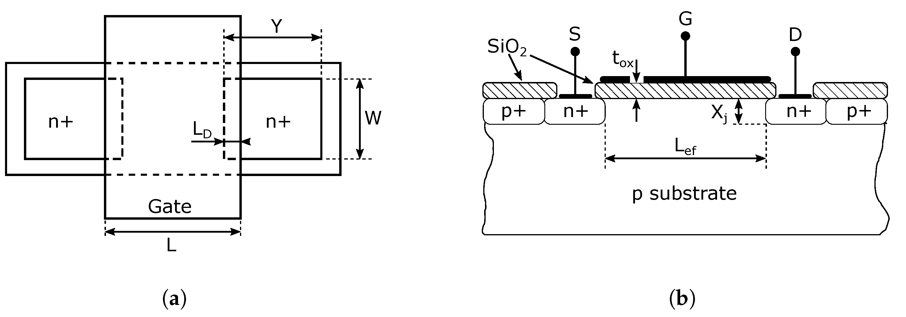
2.1. Model of the MOSFET Transistor for SiGe BiCMOS Technology
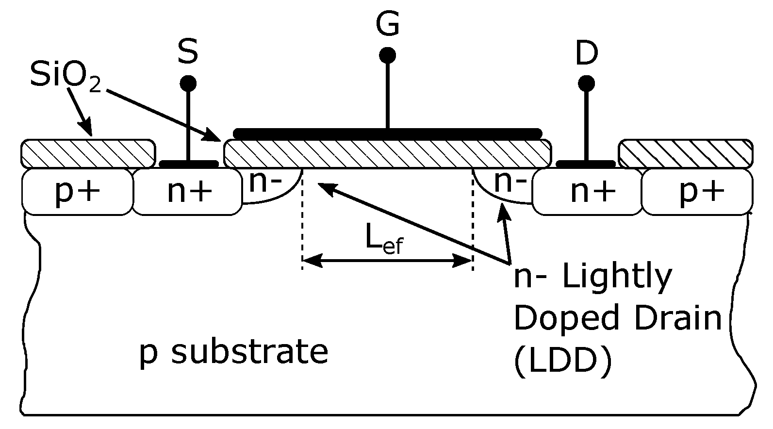
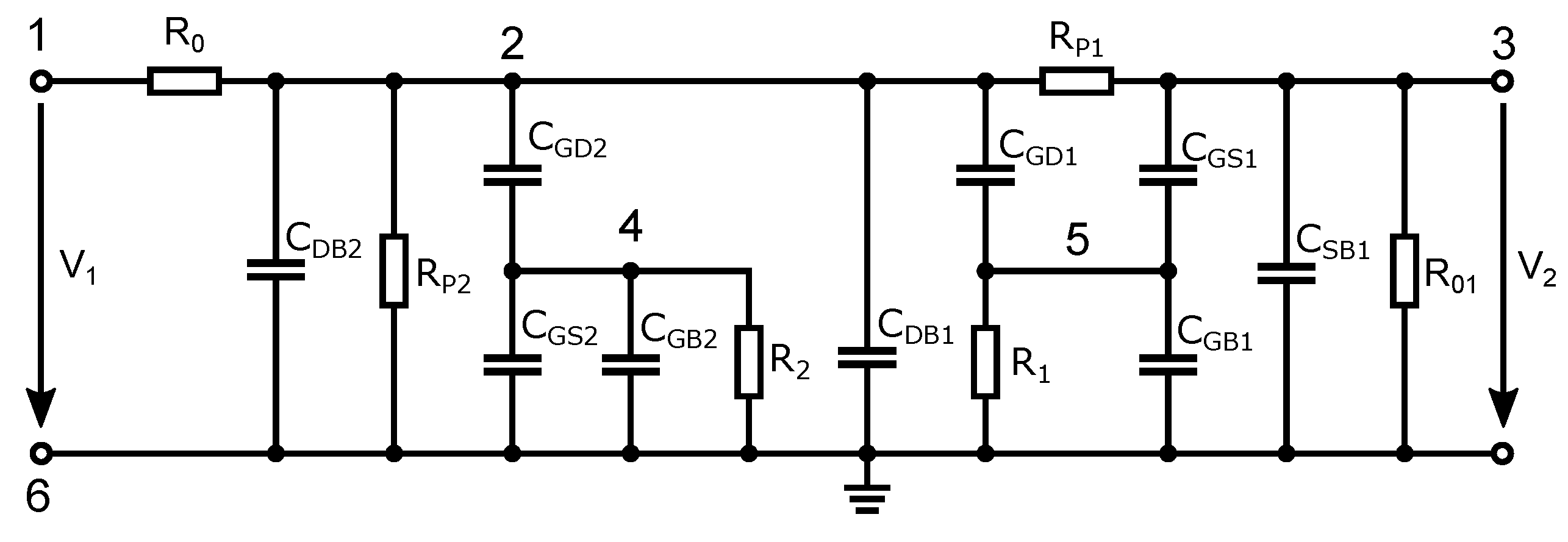
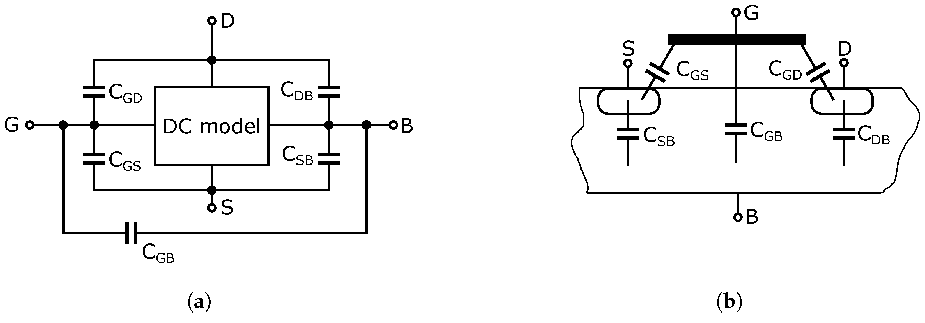
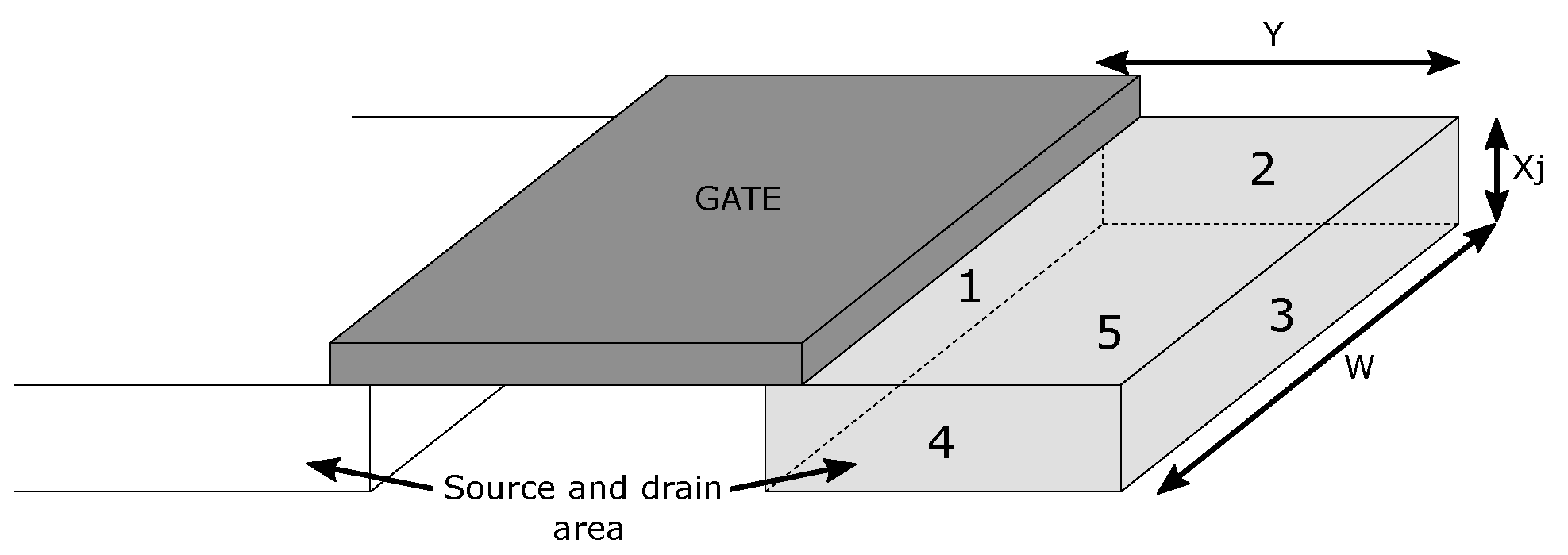
2.2. Parasitic Capacitances in BiCMOS Technology
- The gate capacitance effect, characterized by the parameter;
- The junction capacitances between drain (D)-substrate also called the “bulk” or the body (B) and source (S)-substrate (B) semiconductor junctions.
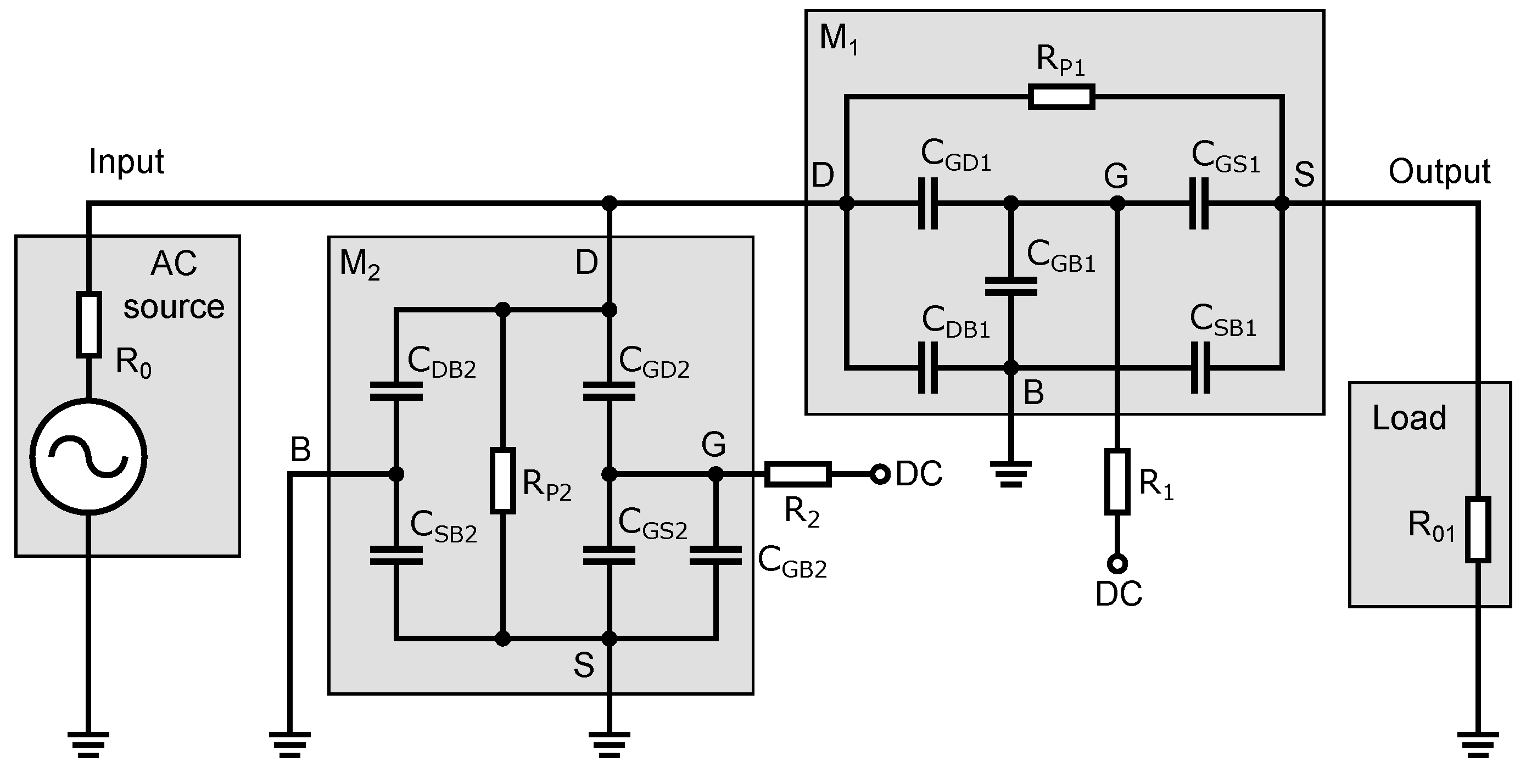
3. Circuit Analysis
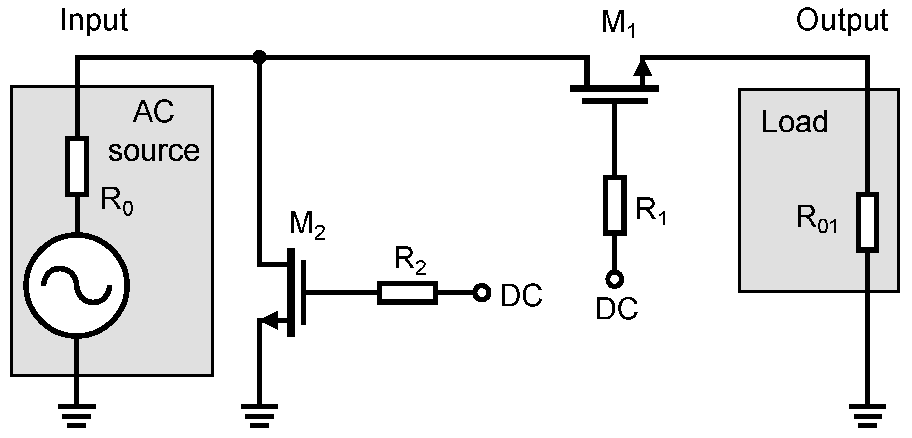
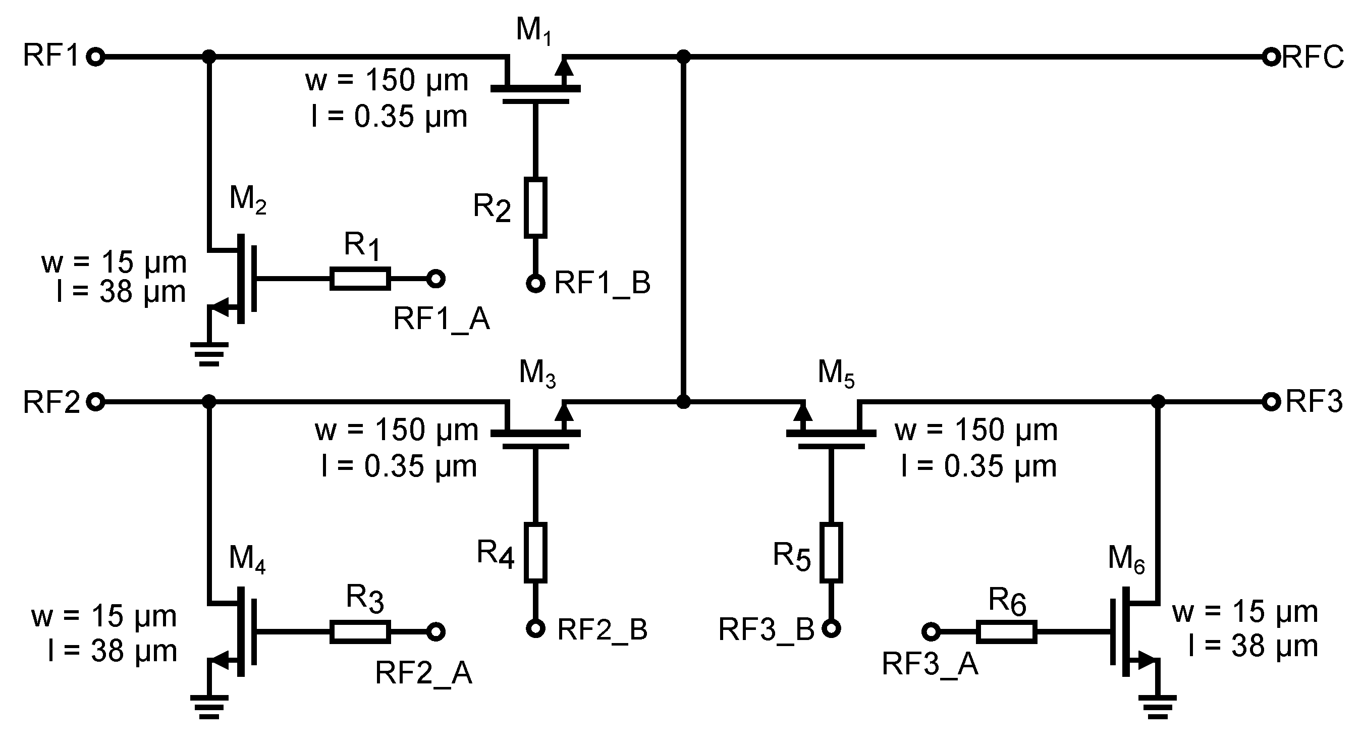
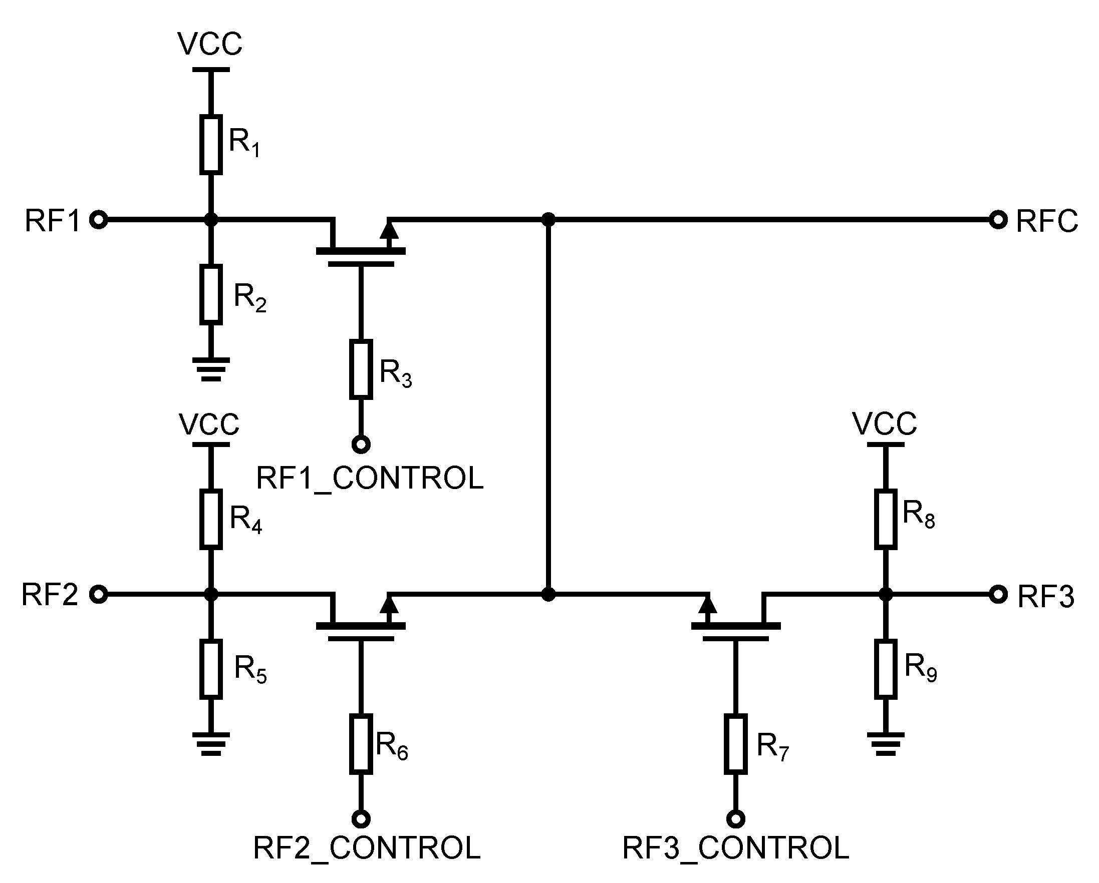
3.1. Analysis and Functional Description of the Switch
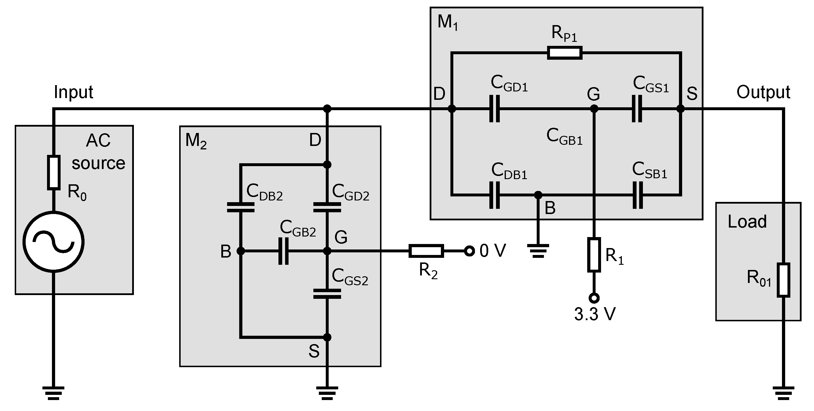
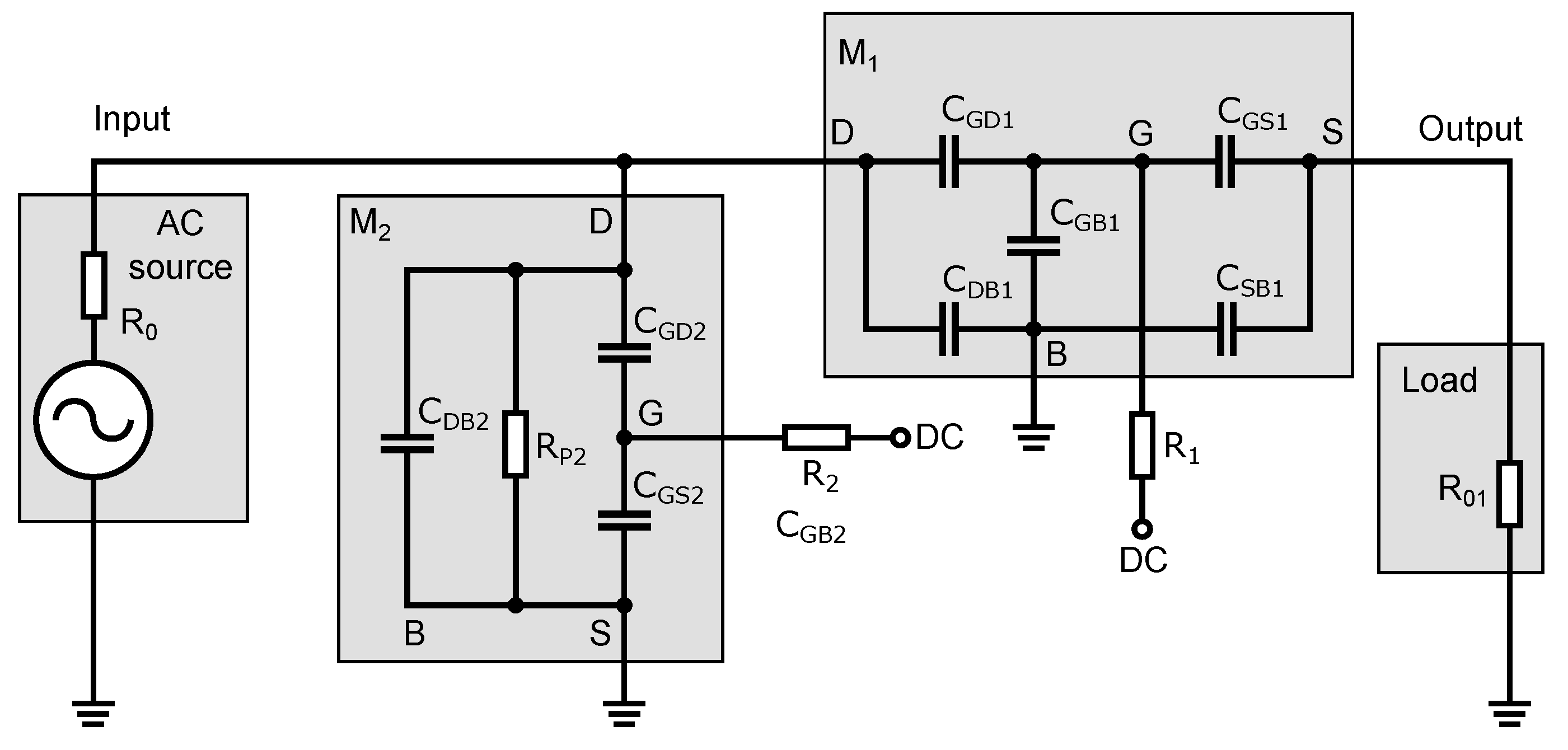
3.2. The Closed State of the Switch
3.3. The Open State of the Switch
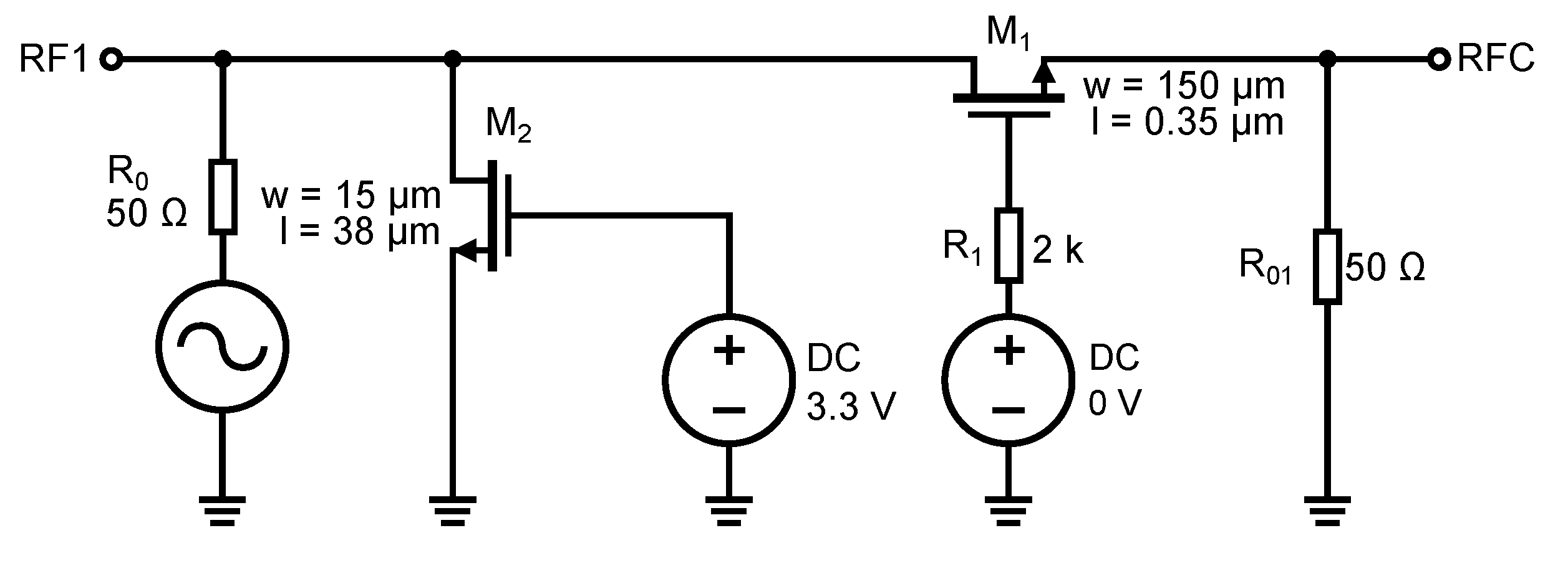
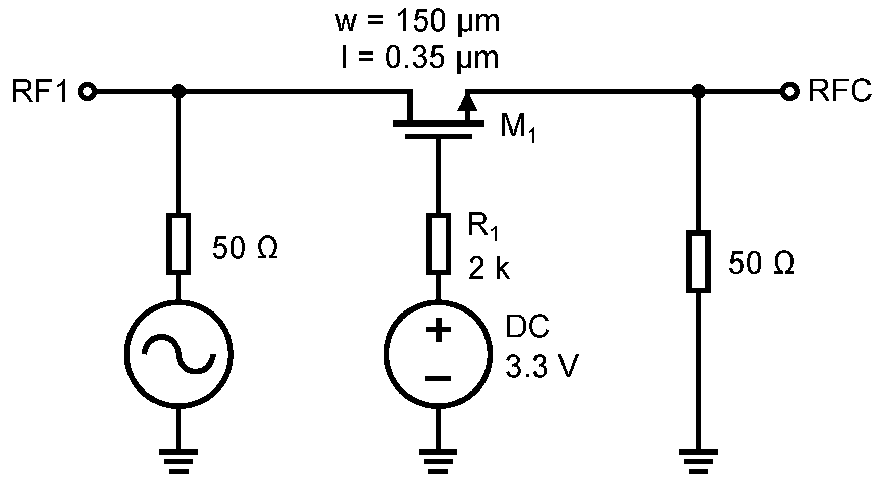
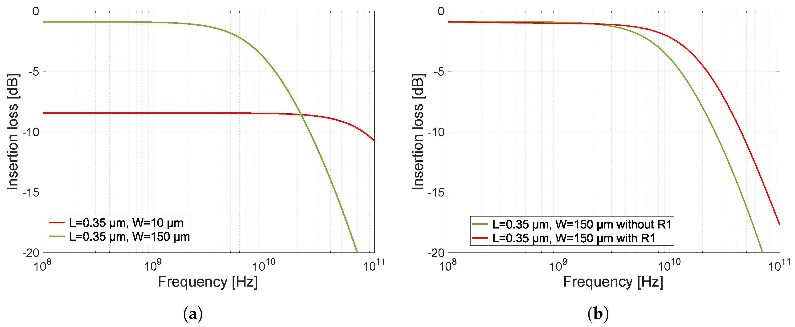
4. Design of the Integrated UWB Switch
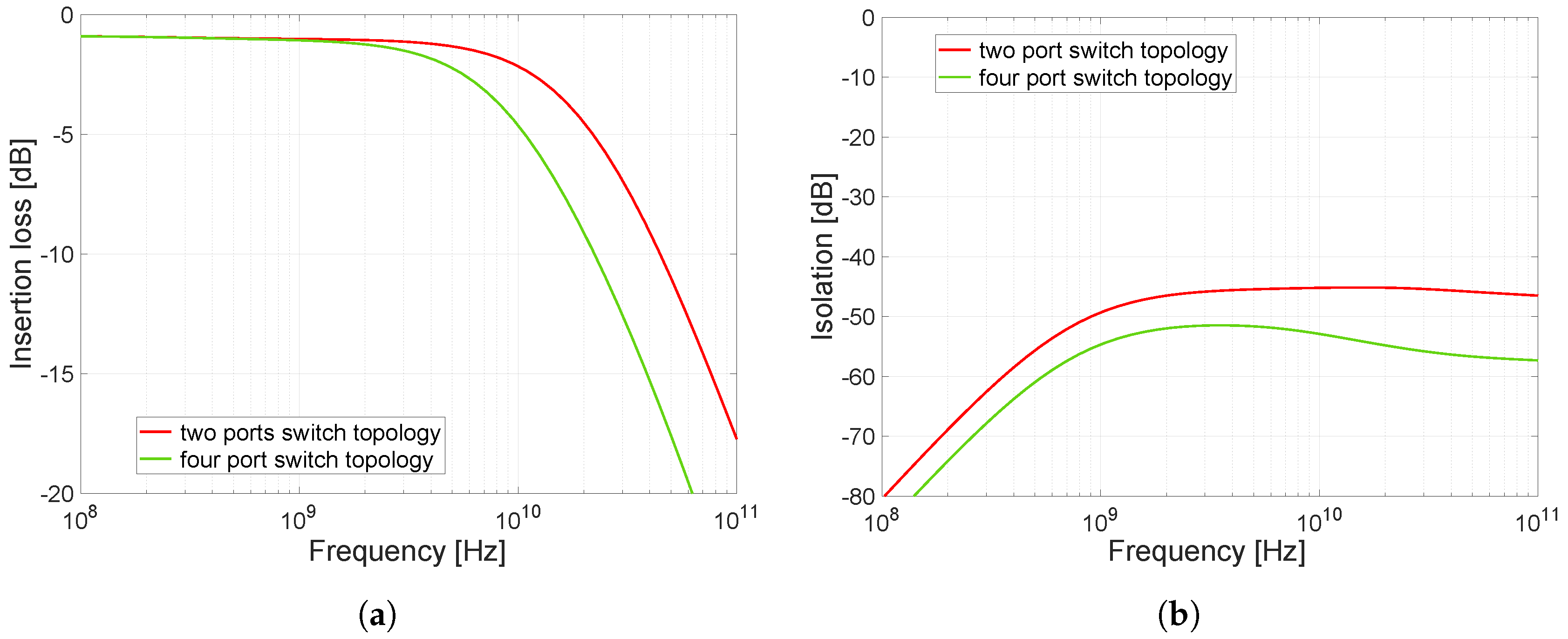
- Minimum, i.e., as small signal attenuation as possible in the closed state (ideally 0 dB);
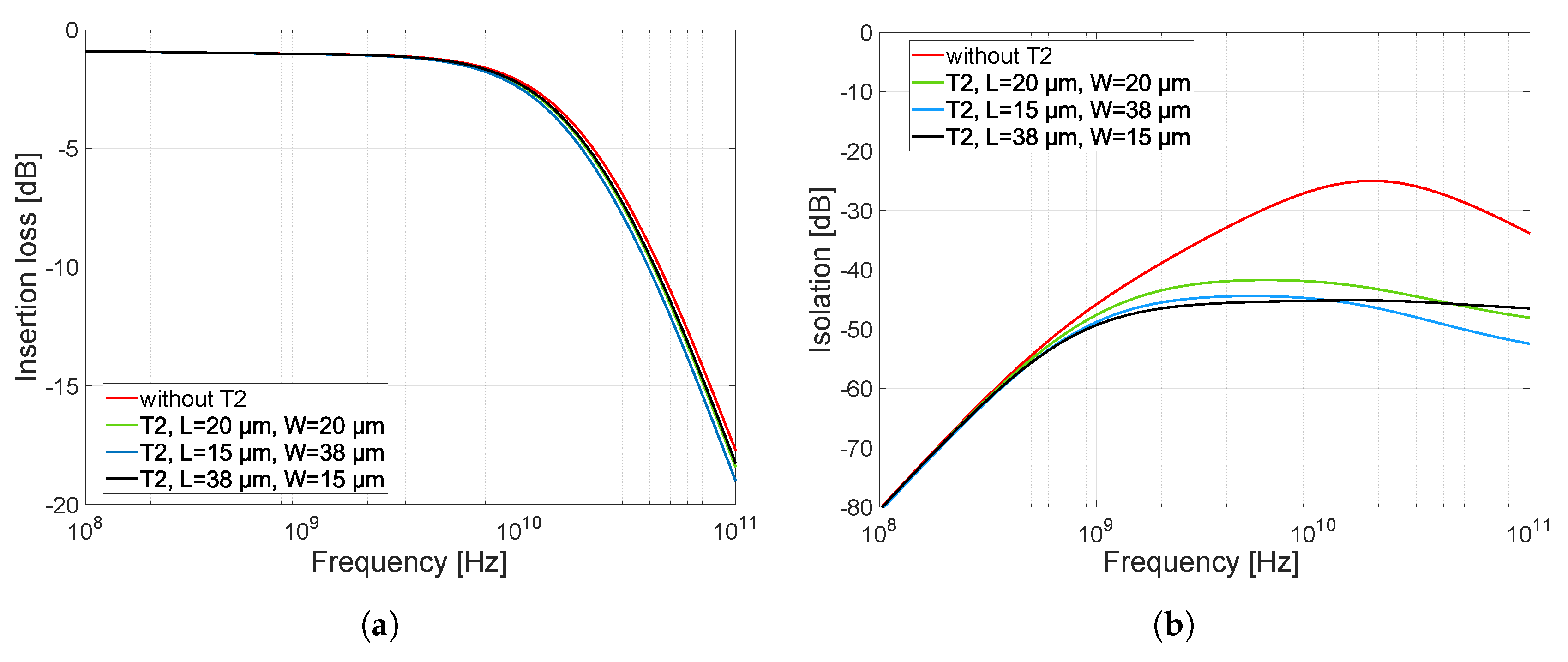
- Maximum on-chip isolation in the open state, preferably below −40 dB;
- A switch frequency bandwidth as wide as possible, from the lowest radio frequencies to a minimum of 10 GHz;
- The highest possible power that the switch can transmit without compression/distortion;
- A control voltage of 3.3 V for logic and switching needs;
- Low power consumption;
- A define the number of outputs, in our case three outputs for the UWB sensor systems (e.g., when switching and configuring an antenna MIMO system) or for switching calibration tools (primarily intended for sensor system calibration).
Design and Simulation of the High-Frequency Part of the Switch
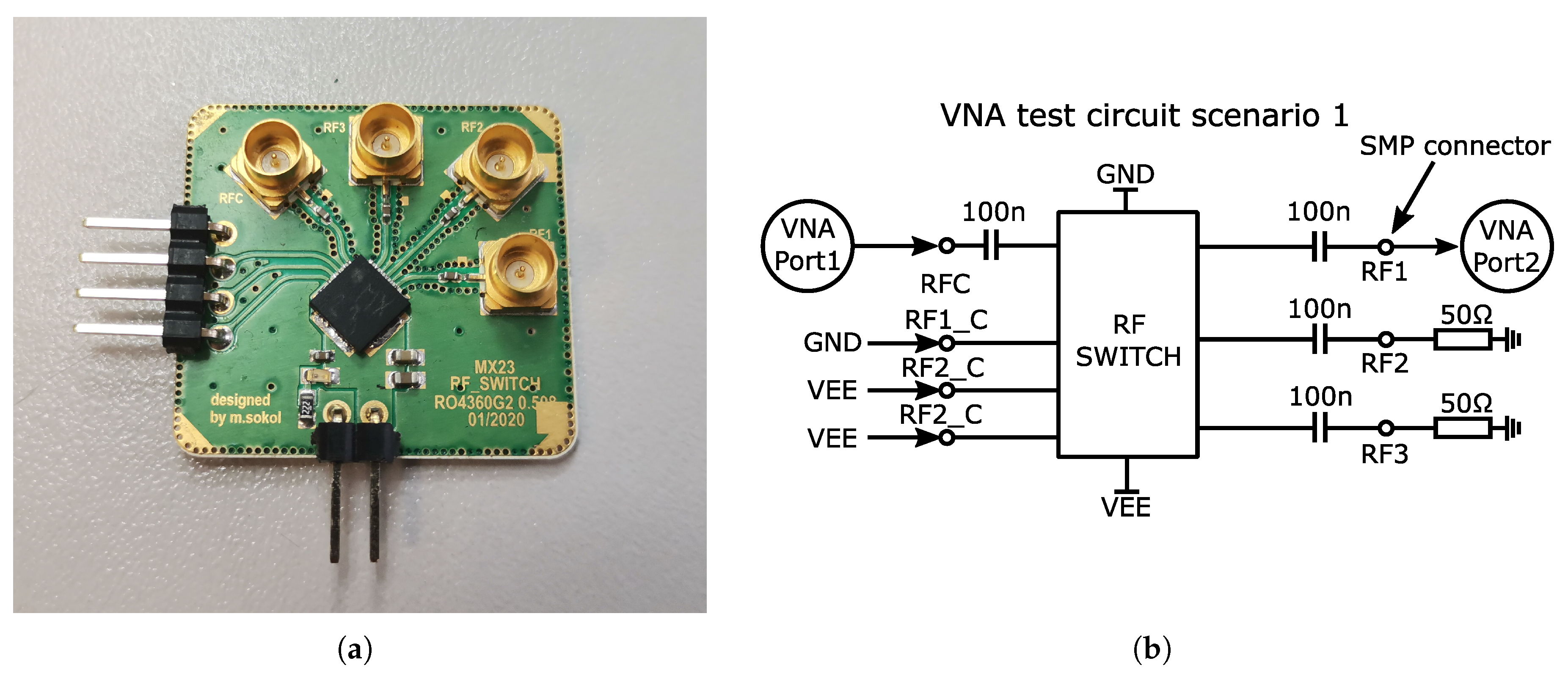
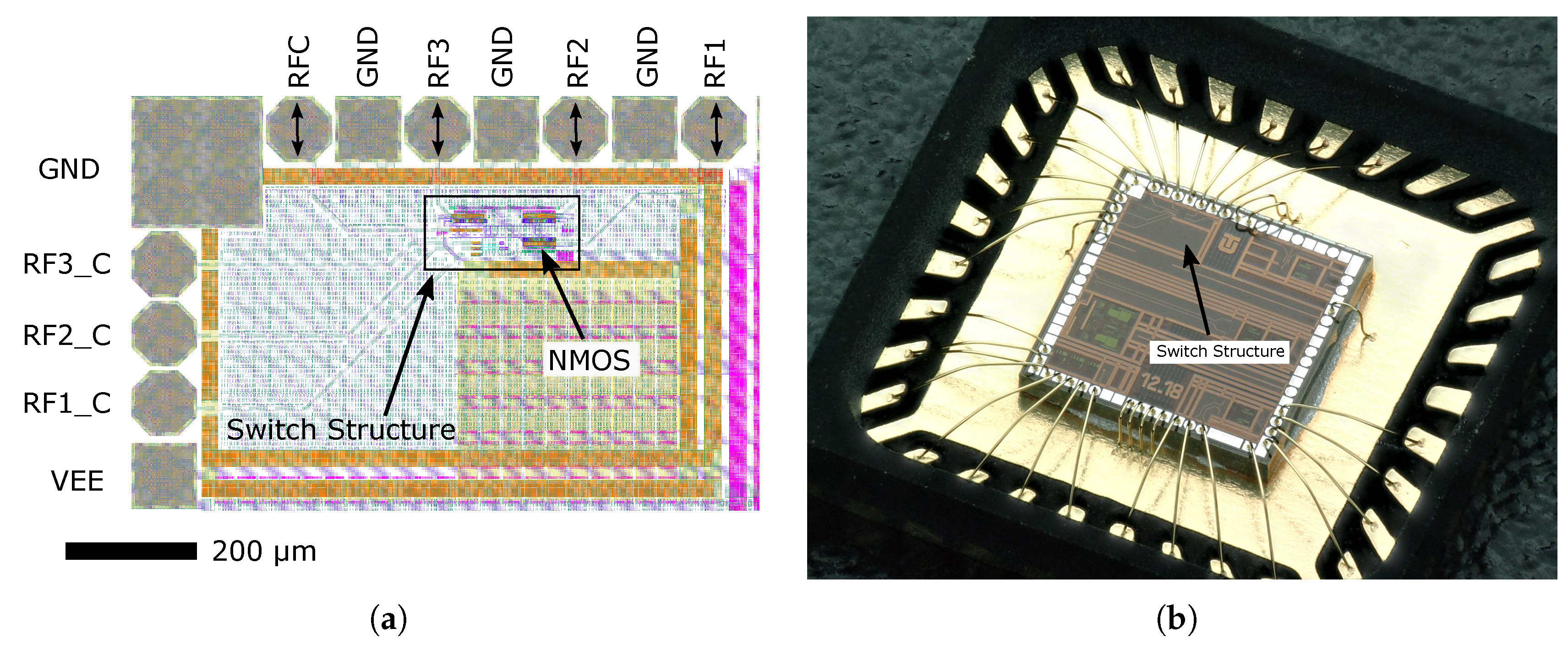
5. Implementation of the Integrated UWB Switch
- Schematic Design—A schematic based design flow and simulation were used. A typical ASIC design implementation includes schematics (consisting of transistor-level Specification & Functional verification) for functional mode as well as the specified technology library. Upon completion of the design schematic, the final netlist (pre-layout netlist) to the physical design for place and route was provided.
- Physical Design—Manual placement and drawing of all devices and structures were used. Once the pre-layout netlist is available, the physical design activities will begin. During the physical design activities, the goal will be to first make sure the routed design will meet the physical design rules (Design Rule Check) and then, if both the schematic circuit and layout circuit match. Upon completion of the routed design, the physical design will provide the post-layout netlist for the final optimization, verification, and evaluation. This uses the simulation same as the simulation of the schematic except for the fact that the results will now include parasitic effects from the actual layout (Extraction). Parasitic capacitances, resistances, and inductances in the layout can strongly affect the performance of a design. Thus to evaluate the effects of parasitics and to gain a higher degree of confidence that a layout will result in a chip that meets the specifications, it is important to run post-layout simulations, as well. In our design flow, we only extracted a layout with parasitic capacitors and resistors (our design environment also supports the extraction of RLC parasitics, but parasitic inductors are not included in the design kit) and only with their values above a certain chosen limit level so that their influence does not significantly affect the operation or accuracy of our design. The performance of a circuit simulated with parasitics accounted for is always worse, although closer to reality, than a schematic that does not include estimated parasitics. Thus, this analysis examines the operation of the design across a range of processes and also different conditions (like voltage, temperature, crosstalk etc.).
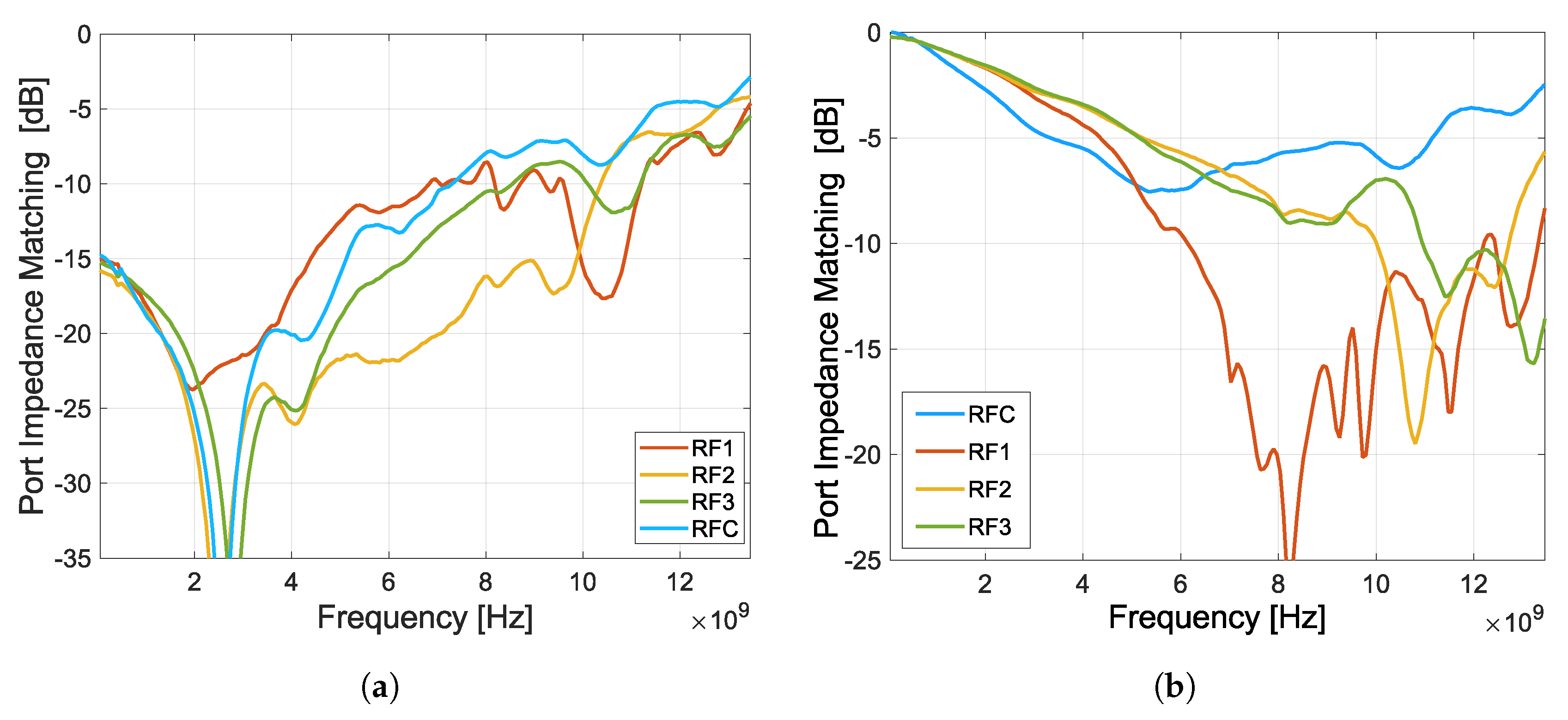
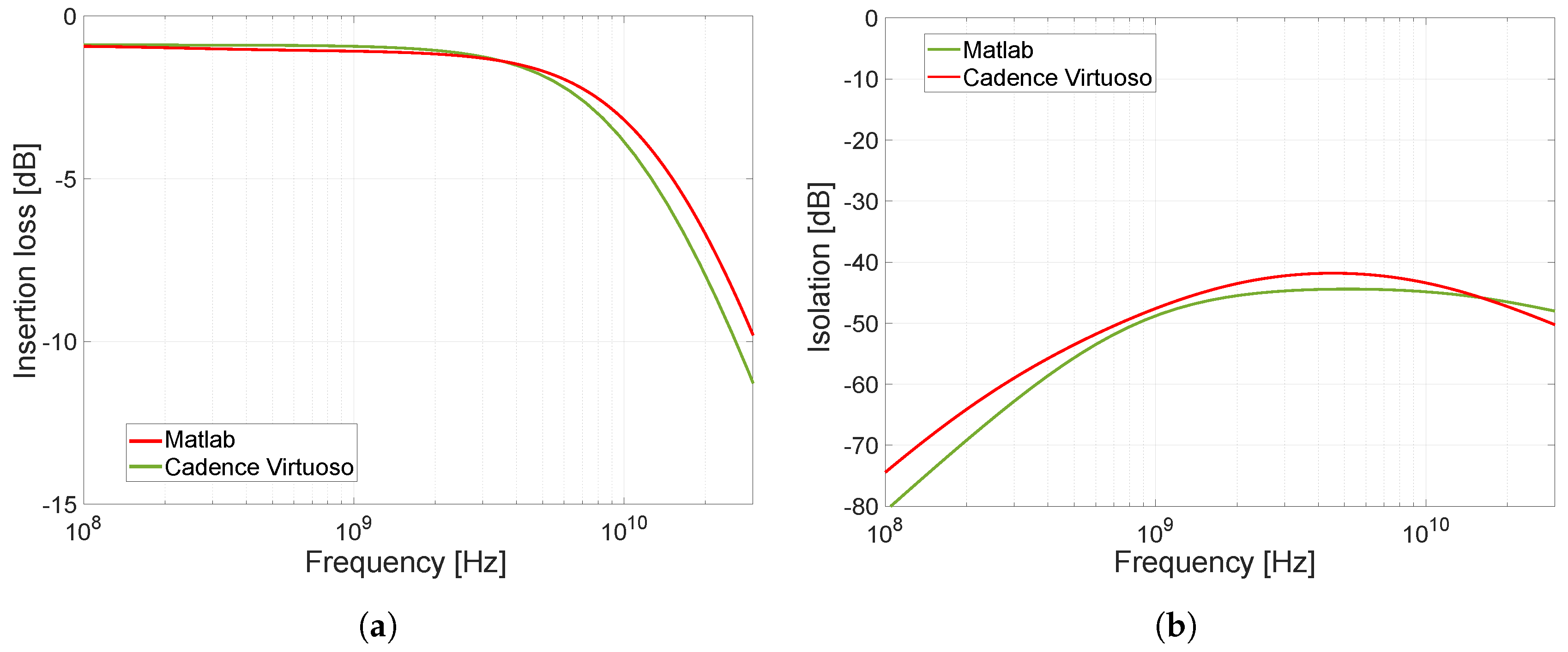
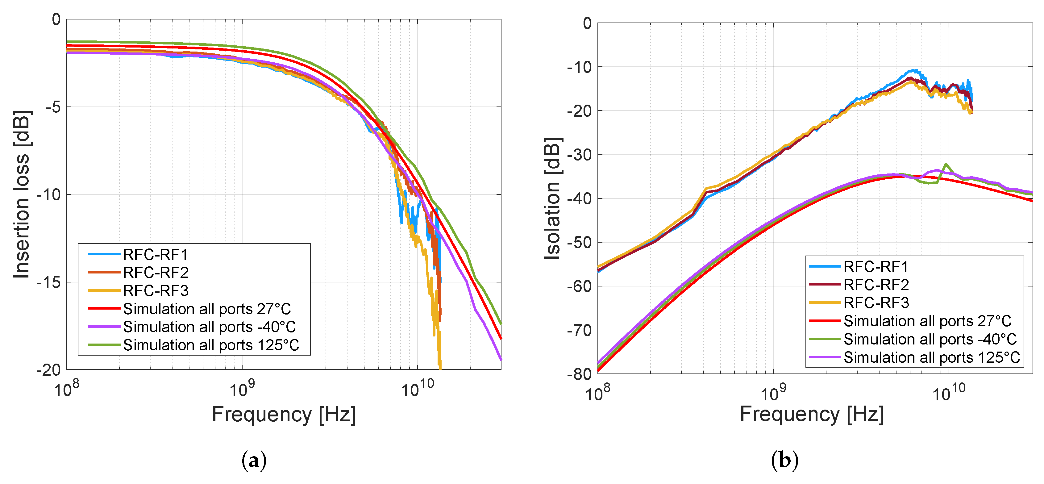
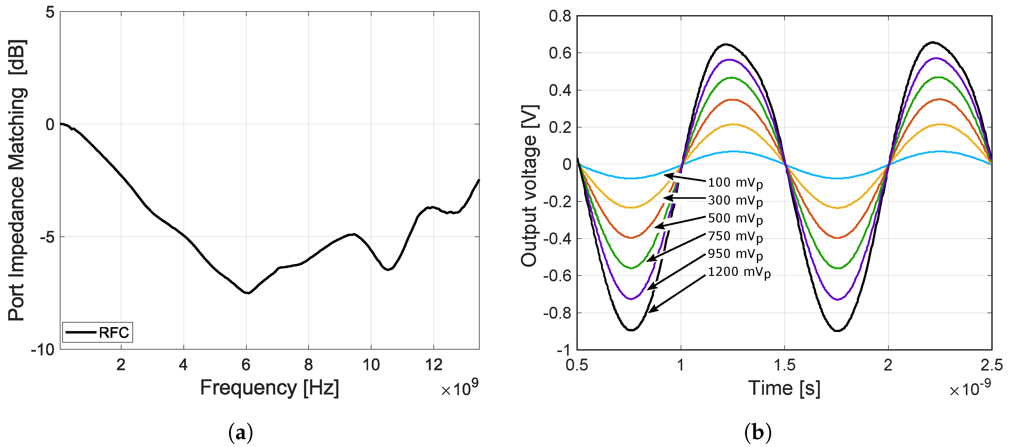
6. Measurement of the Integrated UWB Switch
7. Conclusions
Author Contributions
Funding
Institutional Review Board Statement
Informed Consent Statement
Data Availability Statement
Conflicts of Interest
References
- Sachs, J.; Kmec, M.; Rauschenbach, P.; Herrmann, R.; Schilling, K.; Helbig, M. Toward integrated ultra-wideband MIMO-sensors. In Proceedings of the 2012 The 7th German Microwave Conference, Ilmenau, Germany, 12–14 March 2012; pp. 1–4. [Google Scholar]
- Tinella, C.; Richard, O.; Cathelin, A.; Reaute, F.; Majcherczak, S.; Blanchet, F.; Belot, D. 0.13/spl mu/m CMOS SOI SP6T antenna switch for multi-standard handsets. In Proceedings of the Digest of Papers. 2006 Topical Meeting on Silicon Monolithic Integrated Circuits in RF Systems, San Diego, CA, USA, 18–20 January 2006; p. 4. [Google Scholar]
- Solomko, V.; Oezdamar, O.; Weigel, R.; Hagelauer, A. CMOS RF switch with fast discharge feature. IEEE Solid-State Circ. Lett. 2021, 4, 68–71. [Google Scholar] [CrossRef]
- Kara-Omar, A.; Dragomirescu, D.; Coustou, A.; Plana, R. UWB down-conversion mixer in CMOS 130 nm technology for wireless sensor network applied to aerospace application. In Proceedings of the 2013 European Microwave Integrated Circuit Conference, Nuremberg, Germany, 6–8 October 2013; pp. 192–195. [Google Scholar]
- Slovak, S.; Galajda, P.; Hoffmann, J.; Kocur, D. New ultra-wideband sensor system for measuring the properties of liquid materials. In Proceedings of the 2016 26th International Conference Radioelektronika (RADIOELEKTRONIKA), Kosice, Slovakia, 19–20 April 2016; pp. 309–314. [Google Scholar]
- Pecovsky, M.; Sokol, M.; Galajda, P. 15 th Order M-sequence SoC Radar for Short-Range Sensing. In Proceedings of the 2020 21st International Radar Symposium (IRS), Warsaw, Poland, 5–8 October 2020; pp. 1–5. [Google Scholar]
- Ziga, M.; Galajda, P.; Slovak, S.; Kmec, M. Determination of the quality of frying oil based on UWB impedance spectrometer. In Proceedings of the 2015 16th International Radar Symposium (IRS), Dresden, Germany, 24–26 June 2015; pp. 955–960. [Google Scholar] [CrossRef]
- Galajda, P.; Svecova, M.; Drutarovsky, M.; Slovak, S.; Pecovsky, M.; Sokol, M.; Kocur, D. Wireless UWB sensor system for robot gripper monitoring in non-cooperative environments. In Recent Advances in Intelligent Engineering; Springer: Berlin/Heidelberg, Germany, 2020; pp. 177–207. [Google Scholar]
- Pecovsky, M.; Galajda, P.; Sokol, M.; Kmec, M. Measurement of Opaque Container Contents by an M-Sequence UWB Radar. In Proceedings of the 2020 IEEE International Radar Conference (RADAR), Washington, DC, USA, 28–30 April 2020; pp. 384–388. [Google Scholar]
- Sachs, J. Handbook of Ultra-Wideband Short-Range Sensing; John Wiley & Sons: Weinheim, Germany, 2012. [Google Scholar] [CrossRef]
- Hein, M.; Helbig, M.; Kmec, M.; Sachs, J.; Sachs, J.; di Clemente, F.S.; Stephan, R.; Hamouda, M.; Ussmueller, T.; Weigel, R.; et al. Ultra-wideband active array imaging for biomedical diagnostics. In Proceedings of the 2012 IEEE-APS Topical Conference on Antennas and Propagation in Wireless Communications (APWC), Cape Town, South Africa, 2–7 September 2012; pp. 367–370. [Google Scholar]
- Rovnakova, J.; Kocur, D. Experimental comparison of two UWB radar systems for through-wall tracking application. Acta Electrotech. Inform. 2012, 12, 59. [Google Scholar] [CrossRef]
- Galajda, P.; Pecovsky, M.; Sokol, M.; Kmec, M.; Kocur, D. Recent Advances in ASIC Development for Enhanced Performance M-Sequence UWB Systems. Sensors 2020, 20, 4812. [Google Scholar] [CrossRef] [PubMed]
- Slovak, S.; Galajda, P.; Pecovsky, M.; Sokol, M. Integrated SoC UWB radar with built-in 15-bit M-sequence generator. In Proceedings of the 2018 28th International Conference Radioelektronika (RADIOELEKTRONIKA), Prague, Czech Republic, 19–20 April 2018; pp. 1–4. [Google Scholar]
- Sokol, M.; Galajda, P. Design of a 7-bit Flash AD Converter for M-Sequence UWB Sensor Systems. In Proceedings of the 2021 31st International Conference Radioelektronika (RADIOELEKTRONIKA), Brno, Czech Republic, 19–21 April 2021; pp. 1–6. [Google Scholar]
- Rebeiz, G.M.; Muldavin, J.B. RF MEMS switches and switch circuits. IEEE Microw. Mag. 2001, 2, 59–71. [Google Scholar] [CrossRef]
- Sun, P.; Upadhyaya, P.; Jeong, D.; Heo, D.; Rue, G.S.L. A Novel SiGe PIN Diode SPST Switch for Broadband T/R Module. IEEE Microw. Wirel. Components Lett. 2007, 17, 352–354. [Google Scholar] [CrossRef]
- Parthasarathy, S.; Trivedi, A.; Sirohi, S.; Groves, R.; Olsen, M.; Chauhan, Y.S.; Carroll, M.; Kerr, D.; Tombak, A.; Mason, P. RF SOI Switch FET Design and Modeling Tradeoffs for GSM Applications. In Proceedings of the 2010 23rd International Conference on VLSI Design, Bangalore, India, 3–7 January 2010; pp. 194–199. [Google Scholar] [CrossRef]
- Hindle, P. The state of RF/microwave switches. Microw. J. 2010, 53, 20–36. [Google Scholar]
- Li, X.J.; Zhang, Y.P. Flipping the CMOS switch. IEEE Microw. Mag. 2010, 11, 86–96. [Google Scholar] [CrossRef]
- Li, Q.; Zhang, Y.P. CMOS T/R switch design: Towards ultra-wideband and higher frequency. IEEE J. -Solid-State Circuits 2007, 42, 563–570. [Google Scholar] [CrossRef]
- Cory, R.; Fryklund, D. RF/microwave solid state switches. MPD/Microwave Product Digest. Berlin, Germany. May 2009. Available online: https://rf.cdiweb.com/datasheets/skyworks/4a_rf_microwave_solid_state_switches.pdf (accessed on 3 July 2023).
- Gray, P.R.; Hurst, P.; Meyer, R.G.; Lewis, S. Analysis and Design of Analog Integrated Circuits; Wiley: New York, NY, USA, 2001. [Google Scholar]
- Razavi, B. Design of Analog CMOS Integrated Circuits, 2nd ed.; McGraw-Hill Education: New York, NY, USA, 2017. [Google Scholar]
- Caka, N.; Zabeli, M.; Limani, M.; Kabashi, Q. Impact of MOSFET parameters on its parasitic capacitances. In Proceedings of the 6th WSEAS International Conference on Electronics, Hardware, Wireless and Optical Communications, Stevens Point, WI, USA, 9–12 December 2007; Citeseer: Forest Grove, OR, USA, 2007; pp. 55–59. [Google Scholar]
- Neamen, D.A. Electronic Circuit Analysis and Design; McGraw-Hill: New York, NY, USA, 2001; Volume 2. [Google Scholar]
- Liou, J.J.; Ortiz-Conde, A.; Garcia-Sanchez, F. Analysis and Design of MOSFETs: Modeling, Simulation, and Parameter Extraction; Springer Science & Business Media: New York, NY, USA, 1998. [Google Scholar]
- Sedra, A.S.; Sedra, D.E.A.S.; Smith, K.C.; Smith, K.C. Microelectronic Circuits; Oxford University Press: New York, NY, USA, 1998. [Google Scholar]
- pSemi Corporation. PE42540 UltraCMOS® SP4T RF Switch 10 Hz–8 GHz, pSemi. 2022. Available online: https://www.psemi.com/pdf/datasheets/pe42540ds.pdf (accessed on 1 July 2023).
- Wu, W.; Lam, S.; Chan, M. A wide-band T/R switch using enhanced compact waffle MOSFETs. IEEE Microw. Wirel. Components Lett. 2006, 16, 287–289. [Google Scholar]


| Parameter | Symbol | Typical Values | Unit |
|---|---|---|---|
| n+junction depth | 0.18–0.22 | µm | |
| GATE to NDIFF overlap capacitance | 0.3–0.4 | fF/µm | |
| Typical length of LDD | 0.05L to 0.1L | fF/µm | |
| GATE to LDD overlap capacitance | 0.1–0.15 | fF/µm | |
| Elementary junction capacitance | 0.7–1 | fF/µm2 | |
| Sidewall junction capacitance | 0.2–0.3 | fF/µm | |
| Junction potential | 0.7 | V |
| Parameter | PE42540 [29] | This Work | [30] * |
|---|---|---|---|
| Max. supply voltage | 3.55 V VDD −3.6 V VSS | −4.5 V VEE | - |
| Nominal supply voltage | 3.3 V VDD, 3.3 V VSS | −3.3 V VEE | 3 V VDD |
| Nominal supply current | 200 µA | 2 mA | - |
| Bandwidth | 10 Hz–8 GHz | DC–6 GHz (−3 dB) | DC–6 GHz |
| Insertion loss (1 Ghz) | −1 dB | −2.2 dB | −2.1 dB |
| Isolation (1 Ghz) | −50 dB | −33 dB | −29.5 dB |
| Ports type | Absorptive | Reflective | Reflective |
| Ports number | 4 | 4 | 3 |
| Compression P1dB | 30 dBm | 5 dBm | 10.6 dBm |
| Semiconductor technology | 0.13 µm UltraCMOS | 0.35 µm SiGe BiCMOS | 0.35 µm CMOS |
| Package | QFN32 5 × 5 mm | QFN32 5 × 5 mm | - |
Disclaimer/Publisher’s Note: The statements, opinions and data contained in all publications are solely those of the individual author(s) and contributor(s) and not of MDPI and/or the editor(s). MDPI and/or the editor(s) disclaim responsibility for any injury to people or property resulting from any ideas, methods, instructions or products referred to in the content. |
© 2023 by the authors. Licensee MDPI, Basel, Switzerland. This article is an open access article distributed under the terms and conditions of the Creative Commons Attribution (CC BY) license (https://creativecommons.org/licenses/by/4.0/).
Share and Cite
Jurik, P.; Sokol, M.; Galajda, P.; Drutarovsky, M. Analysis and Implementation of Controlled Semiconductor Switch for Ultra-Wideband Radar Sensor Applications. Sensors 2023, 23, 7392. https://doi.org/10.3390/s23177392
Jurik P, Sokol M, Galajda P, Drutarovsky M. Analysis and Implementation of Controlled Semiconductor Switch for Ultra-Wideband Radar Sensor Applications. Sensors. 2023; 23(17):7392. https://doi.org/10.3390/s23177392
Chicago/Turabian StyleJurik, Patrik, Miroslav Sokol, Pavol Galajda, and Milos Drutarovsky. 2023. "Analysis and Implementation of Controlled Semiconductor Switch for Ultra-Wideband Radar Sensor Applications" Sensors 23, no. 17: 7392. https://doi.org/10.3390/s23177392
APA StyleJurik, P., Sokol, M., Galajda, P., & Drutarovsky, M. (2023). Analysis and Implementation of Controlled Semiconductor Switch for Ultra-Wideband Radar Sensor Applications. Sensors, 23(17), 7392. https://doi.org/10.3390/s23177392