

Optimizing Time Resolution Electronics for DMAPs

 , , , , and
Abstract
1. Introduction
2. State of the Art
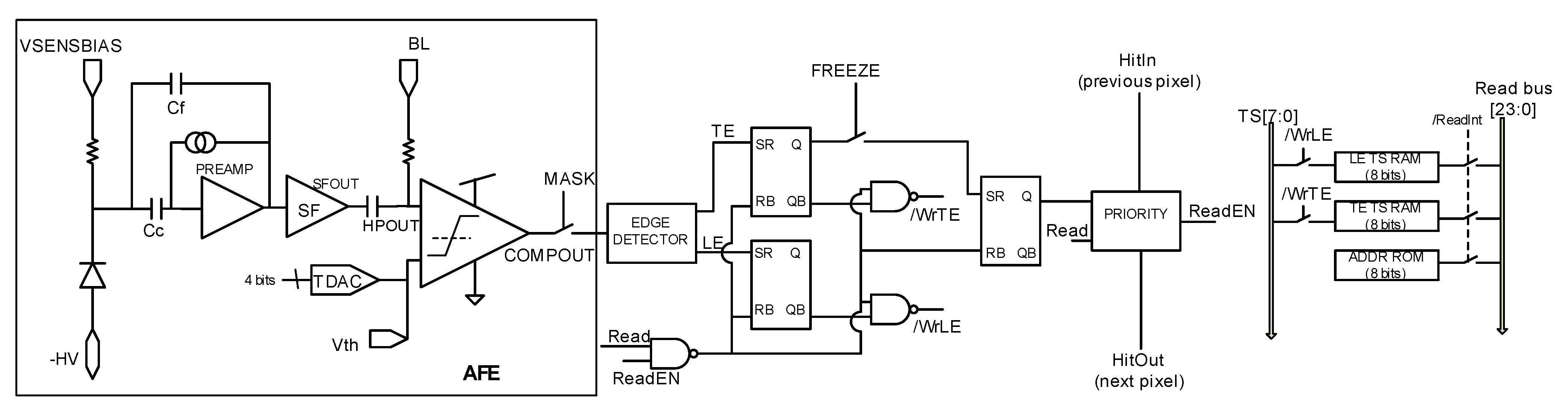
3. RD50-MPW3 Solution
4. Theoretical Analysis for Architecture Optimization
4.1. Increasing the Frequency of the Master Clock
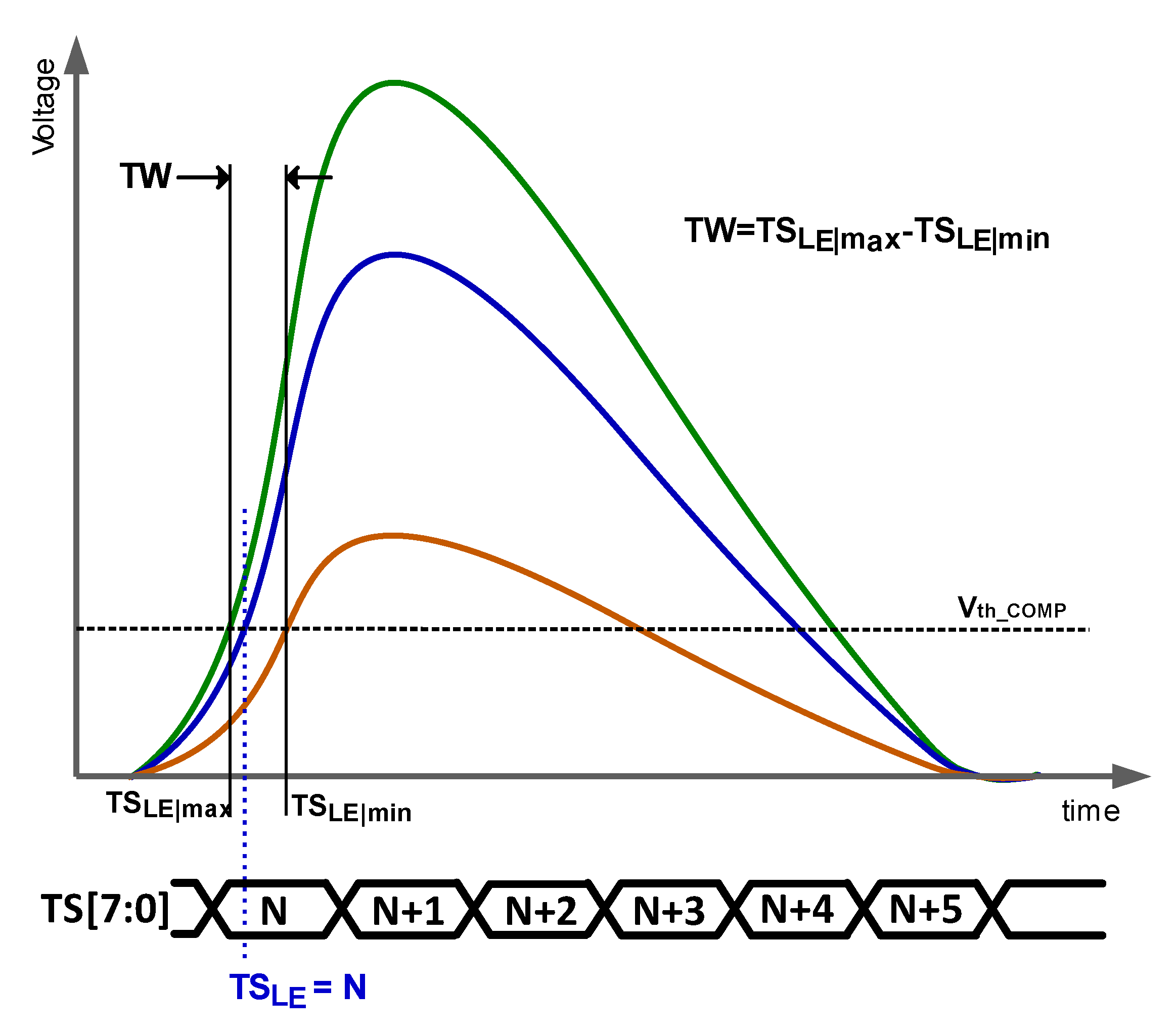
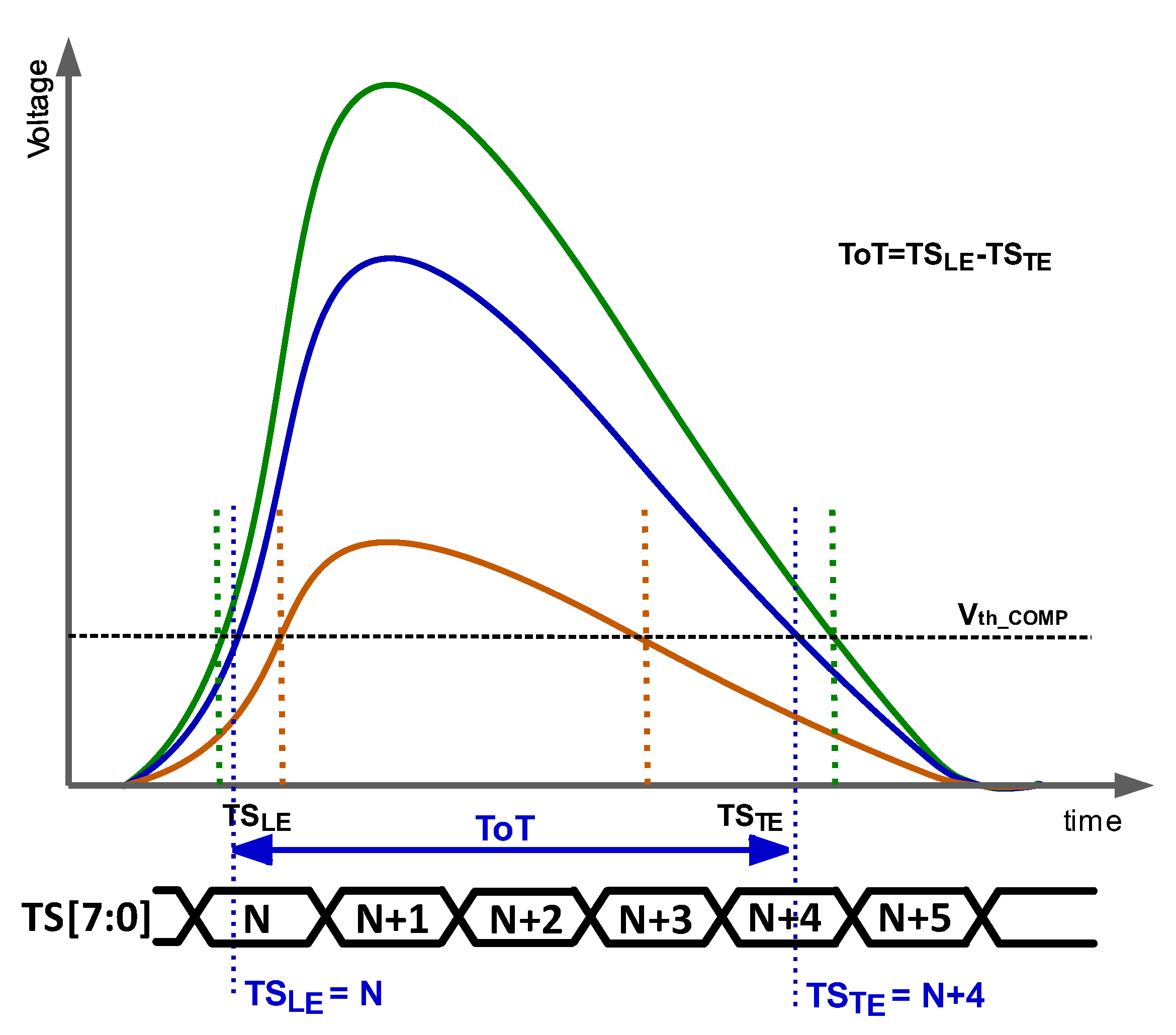
4.2. Optimizing the Number of Stages in the TDC
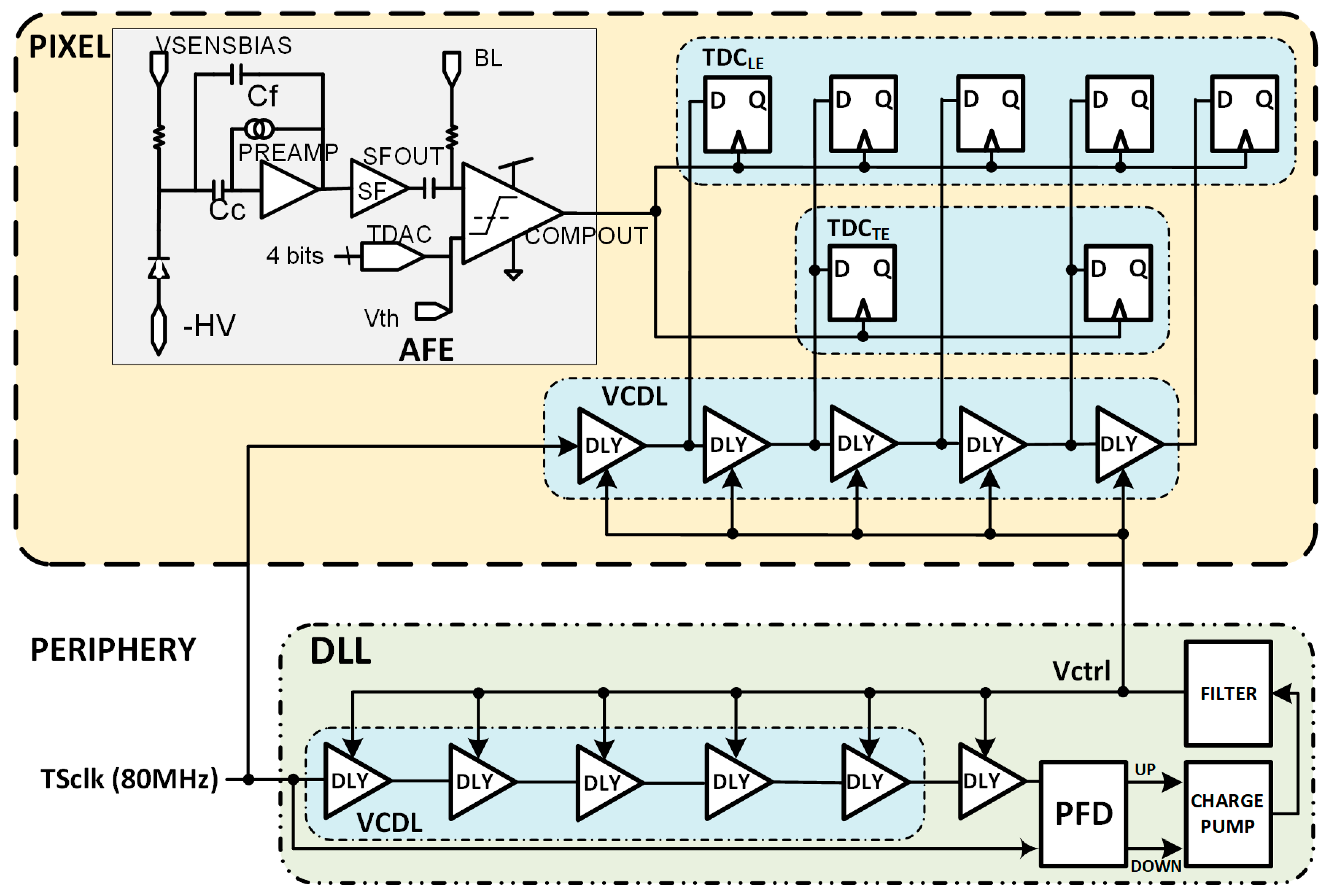
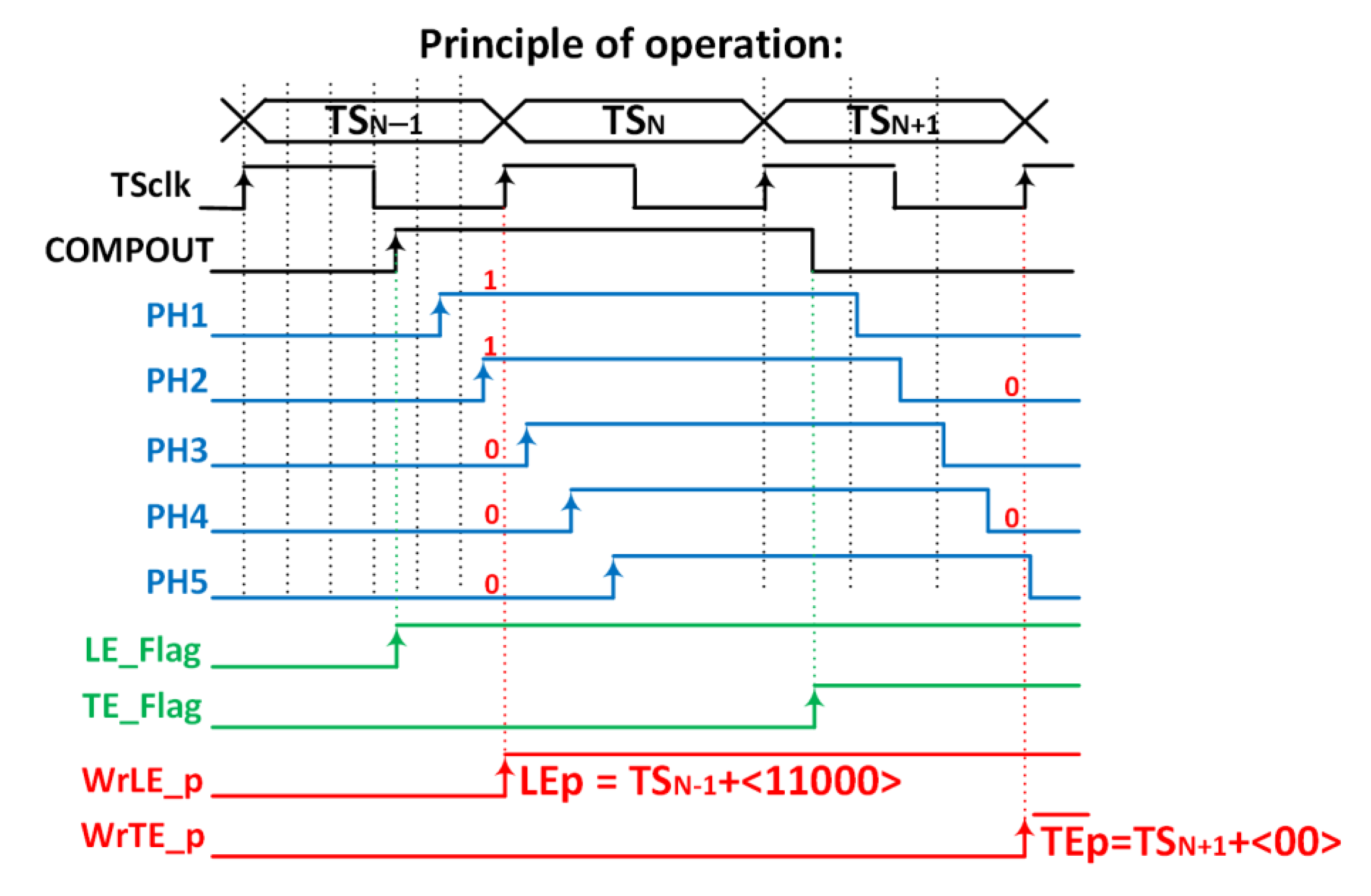
5. Proposed Implementation
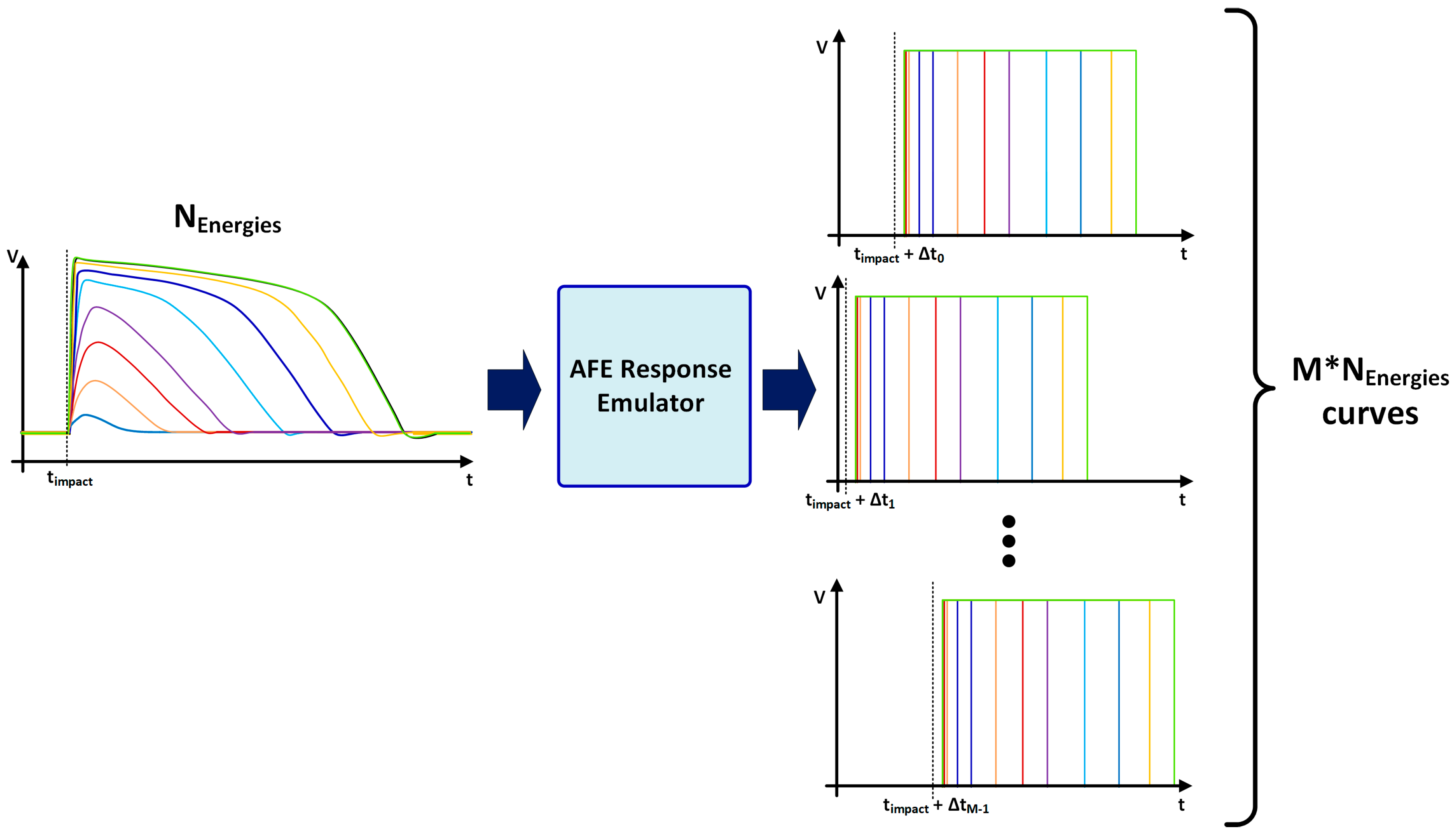
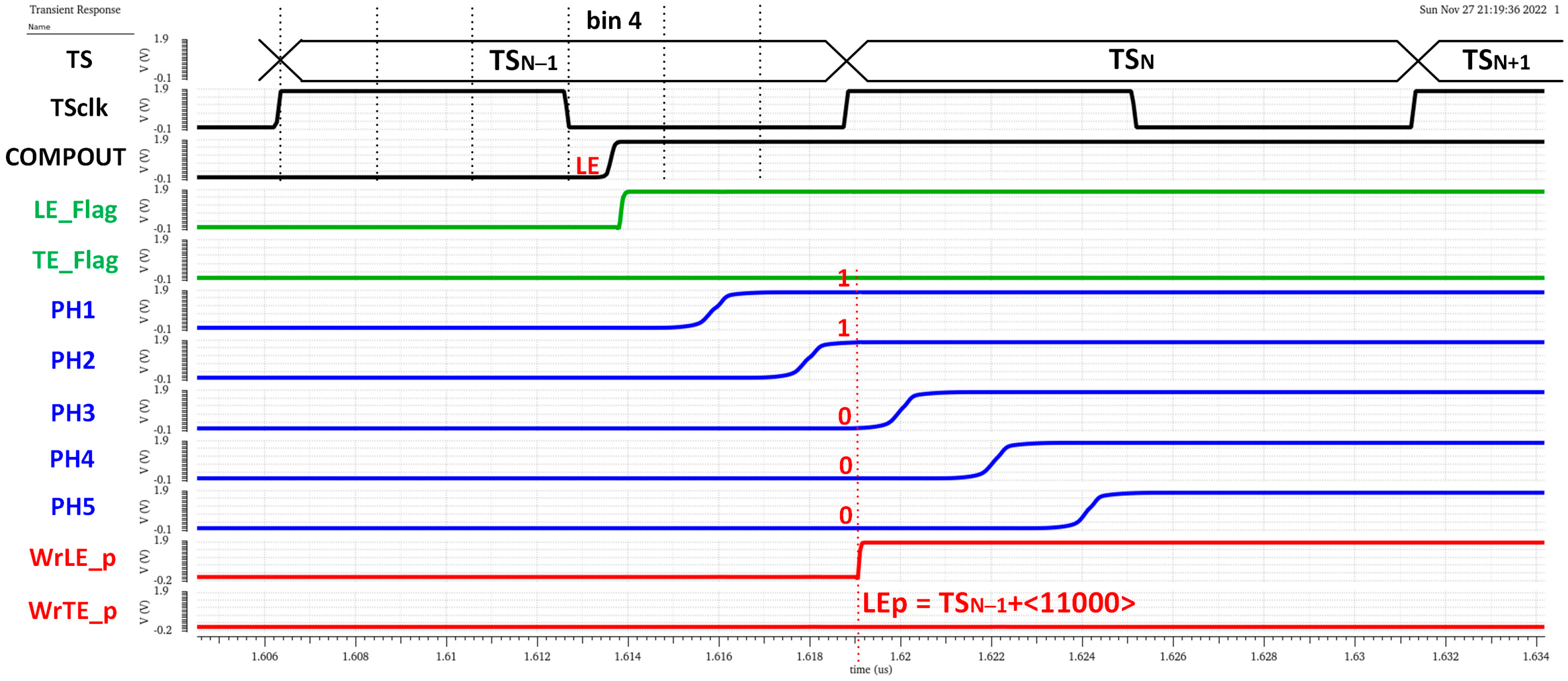
6. Simulation Results
7. Conclusions
Author Contributions
Funding
Institutional Review Board Statement
Informed Consent Statement
Data Availability Statement
Acknowledgments
Conflicts of Interest
Abbreviations
| ADC | Analog-to-Digital Converter |
| AFE | Analog Front-End |
| ALICE | A Large Ion Collider Experiment–Heavy Ion at LHC |
| ATLAS | A Toroidal LHC Apparatus (LHC Collaboration) |
| BL | Base Line |
| CMS | Compact Muon Solenoid (LHC Experiment) |
| CSA | Charge Sensing Amplifier |
| DAC | Digital-to-Analog Converter |
| DLL | Delay-Locked Loop |
| DMAP | Depleted Monolithic Active Pixel Sensor |
| DRAM | Dynamic Random Access Memory |
| HEP | High-Energy Physics |
| LE | Leading Edge |
| LF-AtlasPix | LFoundry-AtlasPix |
| LHC | Large Hadron Collider |
| LHCb | Large Hadron Collider beauty |
| LUT | Look-Up Table |
| MAP | Monolithic Active Pixel Sensor |
| MPW2 | Multi-Project Wafer 2 |
| RAM | Random Access Memory |
| RD50 | Recherche et Développement 50 |
| RD50-MPW2 | Recherche et Développement 50 Multi-Project Wafer 2 |
| RD50-MPW3 | Recherche et Développement 50 Multi-Project Wafer 3 |
| ROM | Read Only Memory |
| SoA | State of the Art |
| TDC | Time-to-Digital Converter |
| TDCLE | Time-to-Digital Converter for Leading Edge |
| TDCTE | Time-to-Digital Converter for Trailing Edge |
| TE | Trailing Edge |
| ToA | Time of Arrival |
| ToT | Time over Threshold |
| TS | Time stamp |
| TSLE | Time stamp of leading edge |
| TSTE | Time stamp of trailing edge |
| TW | Time Walk |
| TWCC | Time-Walk-Compensated Comparator |
| VCO | Voltage-Controlled Oscillator |
| VCDL | Voltage-Controlled Delay Line |
References
- Wunstorf, R. Radiation tolerant sensors for the ATLAS pixel detector. Nucl. Instrum. Methods Phys. Res. A 2001, 466, 327–334. [Google Scholar] [CrossRef]
- Riedler, P.; Anelli, G.; Antinori, F.; Badala, A.; Bruno, G.E.; Burns, M. Production and Integration of the ALICE Silicon Pixel Detector. Nucl. Instrum. Methods Phys. Res. A 2007, 572, 128–131. [Google Scholar] [CrossRef]
- Arndt, K.; Bolla, G.; Bortoletto, D.; Giolo, K.; Horisberger, R.; Roy, A. Silicon sensors development for the CMS pixel system. Nucl. Instrum. Methods Phys. Res. A 2003, 511, 106–111. [Google Scholar] [CrossRef]
- Gys, T. The pixel hybrid photon detectors for the LHCb-rich project. Nucl. Instrum. Methods Phys. Res. A 2001, 465, 240–246. [Google Scholar] [CrossRef]
- Hartmann, F.; Sharma, A. Multipurpose detectors for high energy physics, an introduction. Nucl. Instrum. Methods Phys. Res. A 2012, 666, 1–9. [Google Scholar] [CrossRef]
- Crooks, J.P.; Ballin, J.A.; Dauncey, P.D.; Magnan, A.-M.; Mikami, Y.; Miller, O.; Noy, M.; Rajovic, V.; Stanitzki, M.; Stefanov, K.D.; et al. A Novel CMOS Monolithic Active Pixel Sensor with Analog Signal Processing and 100% Fill Factor. In Proceedings of the 2007 IEEE Nuclear Science Symposium Conference Record, Honolulu, HI, USA, 26 October–3 November 2007; Volume 2, pp. 931–935. [Google Scholar] [CrossRef]
- Hemperek, T. Fully Depleted MAPS in Standard CMOS Technologies. In Proceedings of the Front End Electronics (FEE 2014), Chicago, IL, USA, 21 May 2014; CERN: Geneva, Switzerland, 2014. Available online: https://indi.to/3CgF5 (accessed on 14 April 2023).
- Franks, M.; Casse, G.; Vilella-Figueras, E.; Massari, N.; Vossebeld, J.; Zhang, C. Design Optimisation of Depleted CMOS Detectors Using TCAD Simulations within the CERN-RD50 Collaboration 14th Trento Workshop on Advanced Silicon Radiation Detectors. Available online: https://indico.cern.ch/event/777112/contributions/3314468/attachments/1802907/2941231/mfranks_14th_TREDI.pdf (accessed on 20 April 2023).
- Degerli, Y.; Guilloux, F.; Guyot, C.; Meyer, J.P.; Ouraou, A.; Schwemling, P.; Apresyan, A.; Heller, R.; Mohd, M.; Pena, C. CACTUS: A depleted monolithic active timing sensor using a CMOS radiation hard technology. J. Instrum. 2020, 15, P06011. [Google Scholar] [CrossRef]
- Schimassek, R.; Ehrler, F.; Perić, I. HVCMOS Pixel Detectors—Methods for Enhancement of Time Resolution. In Proceedings of the 2016 IEEE Nuclear Science Symposium, Medical Imaging Conference and Room-Temperature Semiconductor Detector Workshop( NSS/MIC/RTSD 2016), Strasbourg, France, 29 October–6 November 2016. [Google Scholar] [CrossRef]
- Augustin, H.; Berger, N.; Dittmeier, S.; Ehrler, F.; Grzesik, C.; Hammerich, J.; Zimmermann, M. MuPix8—Large area monolithic HVCMOS pixel detector for the Mu3e experiment. Nucl. Instrum. Methods Phys. Res. A 2019, 936, 681–683. [Google Scholar] [CrossRef]
- Heiko, A.; Niklaus, B.; Sebastian, D.; David, M.; Dohun, K.; Lukas, M.; Annie, M.; Marius, M.; Lars, O.; Ivan, P.; et al. MuPix10: First Results from the Final Design. In Proceedings of the 29th International Workshop on Vertex Detectors (VERTEX2020), Tsukuba, Japan, 5–8 October 2020. [Google Scholar] [CrossRef]
- Augustin, H.; Berger, N.; Blattgerste, C.; Dittmeier, S.; Ehrler, F.; Grzesik, C.; Hammerich, J.; Herkert, A.; Huth, L.; Immig, D. Performance of the large scale HV-CMOS pixel sensor MuPix8. J. Instrum. 2019, 14, C10011. [Google Scholar] [CrossRef]
- Blanco, R.; Zhang, H.; Krämer, C.; Ehrler, F.; Schimassek, R.; Mohr, R.C.; Figueras, E.V.; Messaoud, F.G.; Leys, R.; Prathapan, M. IOP: HVCMOS Monolithic Sensors for the High Luminosity Upgrade of ATLAS Experiment. J. Instrum. 2017, 12, C04001. [Google Scholar] [CrossRef]
- Moreno, S.; Alonso, O.; Dieguez, A.; Vilella, E.; Casse, G.; Vossebeld, J. A 28 μW Timing Circuit for a 60 μm 2 HV-CMOS Pixel. In Proceedings of the 2019 XXXIV Conference on Design of Circuits and Integrated Systems (DCIS), Bilbao, Spain, 20–22 November 2019; IEEE: New York, NY, USA, 2019; pp. 1–6. [Google Scholar] [CrossRef]
- Llopart, X.; Alozy, J.; Ballabriga, R.; Campbell, M.; Casanova, R.; Gromov, V.; Heijne, E.H.M.; Poikela, T.; Santin, E.; Sriskaran, V. Timepix4, a large area pixel detector readout chip which can be tiled on 4 sides providing sub-200 ps timestamp binning. J. Instrum. 2022, 17, C01044. [Google Scholar] [CrossRef]
- Heijhoff, K.; Akiba, K.; Ballabriga, R.; van Beuzekom, M.; Campbell, M.; Colijn, A.P.; Fransen, M.; Geertsema, R.; Gromov, V.; Cudie, X.L. Timing performance of the Timepix4 front-end. J. Instrum. 2022, 17, P07006. [Google Scholar] [CrossRef]
- Sieberer, P.; Irmler, C.; Steininger, H.; Bergauer, T. Design and characterization of depleted monolithic active pixel sensors within the RD50 collaboration. Nucl. Instrum. Methods Phys. Res. A 2022, 1039, 167020. [Google Scholar] [CrossRef]
- Zhang, C.; Casse, G.; Massari, N.; Vilella, E.; Vossebeld, J. SISSA: Development of RD50-MPW2: A high-speed monolithic HV-CMOS prototype chip within the CERN-RD50 collaboration. Proc. Sci. 2020, 45, TWEPP2019. [Google Scholar] [CrossRef]
- Henzler, S.; Koeppe, S.; Lorenz, D.; Kamp, W.; Kuenemund, R.; Schmitt-Landsiedel, D. A Local Passive Time Interpolation Concept for Variation-Tolerant High-Resolution Time-to-Digital Conversion. IEEE J. Solid State Circuits 2008, 43, 1666–1676. [Google Scholar] [CrossRef]
- Henzler, S. Time-to-Digital Converters. In Springer Series in Advanced Microelectronics; Springer: Dordrecht, The Netherlands, 2010. [Google Scholar] [CrossRef]


| Specification | Value |
|---|---|
| Maximum in-pixel area occupancy | Minimum * |
| In-pixel I/O additional terminals | Minimum |
| Power density | <250 mW/cm2 |
| Specification | Value |
|---|---|
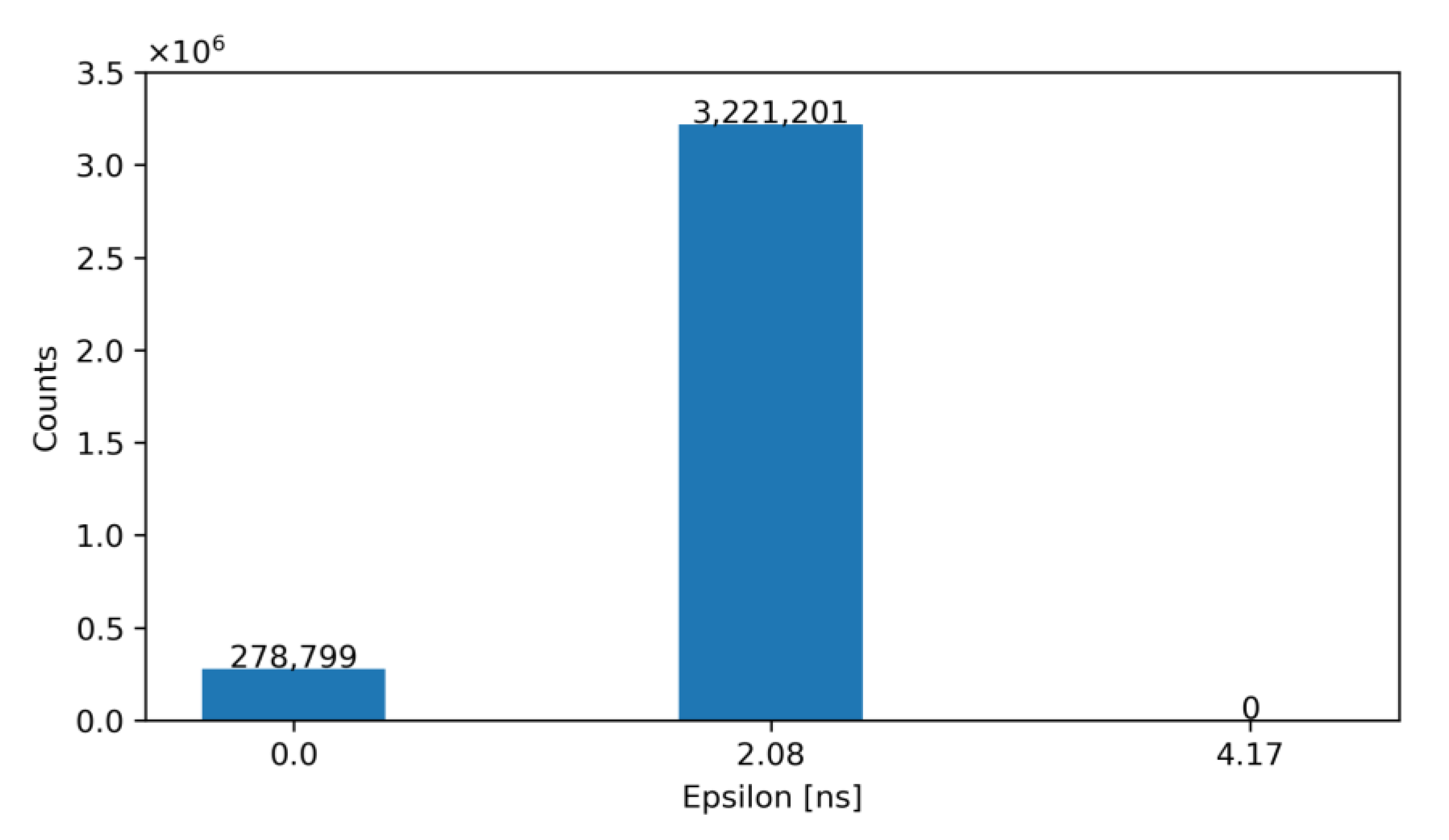
| Time resolution after correction | 2.08 ns |
| Reference clock frequency | 80 MHz (12.5 ns period) |
| NLE | 5 (2.08 ns bin size) |
| NTE | 2 (4.17 ns bin size) |
| In pixel power consumption | Minimum |
| Maximum in-pixel area occupancy | Minimum (max. area 319 µm2) |
| In pixel I/O additional terminals | Minimum |
| Architecture 1 | Architecture 2 | |
|---|---|---|
| NLE acquisition | 5 | 5 |
| NTE acquisition | 5 | 2 |
| Estimated Area [µm2] | 331.5 | 279 |
| Inputs/outputs required | 1/10 | 1/7 |
| εmax [ns] | 2.08 | 2.08 |
| Average ε [ns] | 1.28 | 1.71 |
| Additional quiescent power consumption [µW] | 0 | 0 |
| CAcTμS [9] | MuPix8 [11,12,13] | ATLASPix [14] | O. Alonso et al. [15] | Timepix4 [16,17] | This Work | |
|---|---|---|---|---|---|---|
| Type of solution | Monolithic | Monolithic | Monolithic | Monolithic | Hybrid | Monolithic |
| Manufacturing technology | LF150 nm | AMS aH18 | LF150 nm | LF150 nm | CMOS 65 nm (Readout) | LF150 nm |
| Pixel size | 1 mm2/0.5 mm2 | 80 μm × 81 μm | 150 μm × 50 μm | 60 μm × 60 μm | 55 μm × 55 μm | 62 μm × 62 μm |
| Location of the timing acquisition | Off-chip | Off-pixel | In-pixel | In-pixel | In-pixel | In-pixel |
| Technique | Increase speed amplifier | TWCC Two thresholds Ramp | Analog Sampling + Ramp-ADC | Analog Sampling + TDC (VCDL based) | TDC (VCO based) | TDC (VCDL based) |
| Correction | Offline with ToT (Measured off-chip) | Offline with discriminator delay + 6-bit ToT | Offline with sampled amplitude (48 bits for sampled amplitudes + 16-bit TS) | Offline with sampled amplitude + ToT (5 analog lines + 26 bits ToT) | Offline with ToT (45 bits) | Offline with ToT (23 bits) |
| Additional pixel quiescent power consumption | N/A | - | - | 28 μW | - | None |
| Total quiescent power consumption per pixel | 1.44 mW | - | - | 56 μW | - | 28 μW |
| Additional elements at the periphery | N/A | Discriminator | - | ADC and Phase Generator | VCO (for each 2 × 4 pixels) | DLL |
| Energy range | 4k e− to 40k e− | 1k e− to 10k e− | - | >6k e− | >7k e− | 1k e− to 20k e− |
| Time resolution | 105 ps | 6.5 ns | - | 2.08 ns | 195 ps | 2.08 ns |
Disclaimer/Publisher’s Note: The statements, opinions and data contained in all publications are solely those of the individual author(s) and contributor(s) and not of MDPI and/or the editor(s). MDPI and/or the editor(s) disclaim responsibility for any injury to people or property resulting from any ideas, methods, instructions or products referred to in the content. |
© 2023 by the authors. Licensee MDPI, Basel, Switzerland. This article is an open access article distributed under the terms and conditions of the Creative Commons Attribution (CC BY) license (https://creativecommons.org/licenses/by/4.0/).
Share and Cite
López-Morillo, E.; Luján-Martínez, C.; Hinojo-Montero, J.; Márquez-Lasso, F.; Palomo, F.R.; Muñoz-Chavero, F. Optimizing Time Resolution Electronics for DMAPs. Sensors 2023, 23, 5844. https://doi.org/10.3390/s23135844
López-Morillo E, Luján-Martínez C, Hinojo-Montero J, Márquez-Lasso F, Palomo FR, Muñoz-Chavero F. Optimizing Time Resolution Electronics for DMAPs. Sensors. 2023; 23(13):5844. https://doi.org/10.3390/s23135844
Chicago/Turabian StyleLópez-Morillo, Enrique, Clara Luján-Martínez, José Hinojo-Montero, Fernando Márquez-Lasso, Francisco Rogelio Palomo, and Fernando Muñoz-Chavero. 2023. "Optimizing Time Resolution Electronics for DMAPs" Sensors 23, no. 13: 5844. https://doi.org/10.3390/s23135844
APA StyleLópez-Morillo, E., Luján-Martínez, C., Hinojo-Montero, J., Márquez-Lasso, F., Palomo, F. R., & Muñoz-Chavero, F. (2023). Optimizing Time Resolution Electronics for DMAPs. Sensors, 23(13), 5844. https://doi.org/10.3390/s23135844