Abstract
We describe in detail the construction and characterization of a Peltier-cooled long-wavelength infrared (LWIR) position-sensitive detector (PSD) based on the lateral effect. The device was recently reported for the first time to the authors’ knowledge. It is a modified PIN HgCdTe photodiode, forming the tetra-lateral PSD, with a photosensitive area of 1 × 1 mm2, operating at 205 K in the 3–11 µm spectral range, capable of achieving a position resolution of 0.3–0.6 µm using 10.5 µm 2.6 mW radiation focused on a spot of the 1/e2 diameter 240 µm, with a box-car integration time of 1 µs and correlated double sampling.
1. Introduction
A position-sensing detector (PSD) is a photosensor that detects the position of a light spot on its surface. A PSD enables precise and fast beam alignment and tracking in a variety of applications [1], such as active beam stabilization, optical remote-control devices, infrared (IR) range finders, target detection and tracking, missile interception, IR countermeasures, optical switches, and measurements of vibrations, distortions, and lens refraction/reflection.
The motivation for the responsivity spectral range of up to 10–11 μm, embracing a significant portion of the LWIR band (wavelength λ = 8–14 µm), includes detection and tracking of distant objects, where the LWIR may be preferred to the MWIR (λ = 3–5 µm) and a shorter wavelength due to less aerosol scattering and better performance in environments with dust, fog, or winter haze; higher immunity to atmospheric turbulence; and reduced sensitivity to solar glints and fire flares [2] (p. 5).
LWIR PSDs can also be applied in positioning systems with detection in the LWIR band, especially when LWIR laser beams are used, e.g., in optical communication in free space, in industry using high-power CO2 lasers for hard-material treatment, or in nondestructive inspection and metrology tools. There are numerous medical, industrial, and military applications in the LWIR range [3].
Owing to the frequent requirement for fast and accurate position detection and tracking, PSDs based on fast photon detectors, such as photodiodes, are often preferred to thermal PSDs–quadrant detectors or dense arrays, the acceptable sensitivity of which is achieved at the expense of their slow response times of the order of milliseconds and more [4] (p. 57) [5].
PSDs with the best parameters in terms of position sensitivity and linearity use the lateral photoelectric effect (L-PSD devices) [1,6,7,8]. L-PSDs are single-element detectors of various types and materials, p-n photodiodes or heterostructures, also field-effect phototransistors, where the built-in or externally supplied electric field, perpendicular to the substrate, enables the separation of photogenerated electrons and holes, which next spread laterally in a resistive layer, which will be described later on [7,8,9].
The lateral photoelectric effect was originally described by Schottky in 1930 [10], rediscovered and further elaborated by Wallmark in 1957 [11], and described by Lucovsky in 1960 with analytical equations [12], which help interpret the photoelectric effects observed in nonuniformly irradiated p-n junctions. Developments in the field have since been achieved by many researchers, including the optimization of a PSD construction [13,14] and the shape of electrodes in particular [15].
The main advantage of the L-PSD over photon quadrant detectors (QDs) [16,17], which have been used so far as fast Peltier-cooled PSDs for the LWIR band, is that L-PSD performance is much less dependent on the light-spot intensity distribution. In the case of the L-PSD, the lateral extent of the position measurement span corresponds to the side length of the photosensitive area, while in the case of the QD it corresponds to the diameter of the light spot. Hence, the position linearity is much greater for the L-PSD than for the QD for a given photosensitive area. The L-PSD may also replace a linear array detector, e.g., in compact spectrometers [7].
Previous LWIR L-PSD designs have used cryogenic cooling [6], which is common for LWIR detectors, as it reduces their electric charge thermal generation-recombination (G-R) noise below the level determined by the 300 K thermal background, allowing background-limited performance (BLIP). A cryo-cooler, though, makes the detector assembly bulky, expensive, and often less convenient to operate. Therefore, we decided to explore the possibility of position detection of 10–11 µm radiation at a higher operating temperature, ca. 200 K, achievable by Peltier mini-coolers–small, rugged devices with an operating life of about 20 years and a supply power below 2 W. This is perhaps the first demonstration of such an operation, carried out here on a HgCdTe photodiode with a photosensitive area of 1 × 1 mm2, large for this spectral range and operating temperature, at reverse bias 0.16 V/50 mA. However, power-consuming cooling and bias are also not desirable for portable and integrated devices.
The current L-PSD performance for the IR range of λ < 2 µm (SWIR) may be used as a first benchmark for LWIR PSD development. This includes position resolution of about 0.1 µm normalized to a photosensitive area 1 mm in size, with response times on the order of one to several tens of microseconds and excellent position linearity, with nonlinearity < 2%, obtained without cooling at 0 V bias [1,8,18,19].
SWIR detectors, including L-PSDs, benefit from wide-bandgap semiconductors, used as radiation absorbers. They require neither cooling nor bias to achieve BLIP. SWIR L-PSDs have been commercially available for several decades at a moderate price [9,19]. On the other hand, uncooled or Peltier-cooled LWIR photon detectors suffer from huge thermal generation noise. Their sensitivity is several orders of magnitude lower than that of the wide-gap devices. This is true even for BLIP LWIR detectors, because of the low energy of LWIR photons, about 0.1 eV, comparable to the constant kT = 0.026 eV of the Boltzmann distribution at T = 300 K, resulting in high (300 K) thermal background flux and noise in this spectral range. This is exacerbated by the contribution of nonradiative thermal G-R mechanisms, still playing a role in many LWIR uncooled or Peltier-cooled detectors. The nonradiative high thermal G-R rate in LWIR absorbers results from the low energy of transition of electrons between energy levels, corresponding to the low energy of the absorbed LWIR photons. The thermally generated dark currents of uncooled or Peltier-cooled LWIR photon detectors can be very high if they are not blocked by special barriers in bandgap-engineered structures.
Figure 1 schematically illustrates the principle of operation of the lateral effect photodiode used here. It is a modified PIN photodiode made of LWIR HgCdTe. The inter-band absorption of IR in the absorber layer generates electron–hole pairs, collected as a photocurrent. The device is shaped as a mesa structure, where the lower cathode layer forms the resistive layer acting as the current divider, while the upper anode layer is a common contact. The photocurrent is divided between four cathode metal electrodes in proportion to the resistances of the photocurrent paths between the illuminated region and the electrodes in one resistive layer. Thus, this is the tetra-lateral type (TL-PSD) of L-PSD [13]. In the applied configuration, a pair of cathode electrodes is extended along the opposite edges of the mesa structure, parallel to each other and perpendicular to the same electrodes of the second pair.
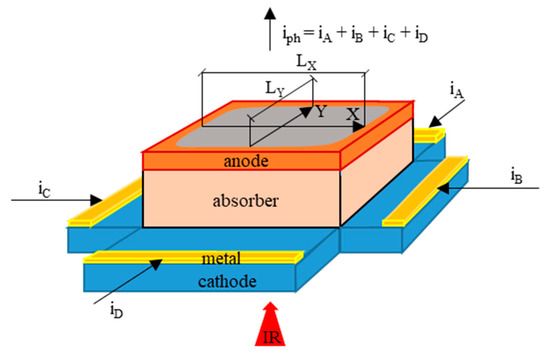
Figure 1.
Principle of operation of the PSD tetra-lateral photodiode (adapted with permission from Ref. [20]; copyright: 2022, SPIE). The photosensitive area is in grey. iA, iB, iC, and iD are the photocurrents flowing to the respective preamplifiers of channels A, B, C, and D.
With Peltier modest cooling to 205 K, the photodiode resistance at 0 V bias is low (<1 Ω) and dominated by the parasitic series resistance, due to the high thermal G-R. The device must be reverse biased to maximize the differential impedance of the photodiode, which is critical to the performance–sensitivity and linearity–of the LWIR L-PSD.
Assuming perfect position linearity, the transverse position (X, Y) of the light spot gravity center is determined by subtracting the signals from the opposite cathode electrodes (channels) and dividing this difference by the sum of these signals (adapted with permission from Ref. [20]; copyright: 2022, SPIE):
where XPSD and YPSD are the Cartesian coordinates of the radiation beam spot position determined from the TL-PSD signals, i.e., the UA, UB, UC, and UD voltages at respective channel preamplifier outputs. The preamplifiers integrate the photocurrent, giving the output voltage proportional to the input radiation pulse energy. The scale factors kX and kY are proportional to the resistance length L ≈ LX ≈ LY ≈ 1 mm (Figure 1). If the dark current of the photodiode is significant, kX and kY are also affected by the dark current and energy of the radiation pulses. In this case, for kX and kY to be constant, the radiation pulse energy should be constant too [7]. The resistance lengths LX and LY represent the linear size of the detector photosensitive area in the X and Y directions, respectively, where the TL-PSD signals change with the respective X and Y position shifts, preferably in linear proportion.
The nonuniformities in the photodiode material layers influence the distribution of the photocurrent between the cathode electrodes and thus cause an error in the light spot position measurement. The position signal error can be corrected using calibration and postprocessing, providing the position measurement noise is low enough. However, time-consuming corrections are not desired in view of the required fast position signal response. Thus, the manufacturing process quality, ensuring the uniformity of the material layers and interfaces, is a key factor.
Even assuming the uniform material layers and the ohmic contacts of the electrodes to the resistive layer, the position linearity and the resulting error of the position estimation using Formulas (1) and (2) worsen with an increase in the size of the light spot and the distance of its gravity center from the middle of the detector active area, depending on the shape and configuration of the electrodes on the resistive layer and the contribution of the series impedance to the total impedance of the detector. Nonlinear effects and corrections realizable by simple fast analog electronics are described in [21].
The position resolution of a PSD is the minimum detectable displacement of a light spot [7,9]. This means that it is related to the signal-to-noise ratio of the detector and read-out electronics. The position resolution can be assessed using the standard deviations and of the position coordinates XPSD and YPSD, respectively (adapted with permission from Ref. [20]; copyright: 2022, SPIE):
where , , , and are the root-mean-square (rms) noises at the respective channel outputs. It is assumed that the noises from the individual channels are uncorrelated with each other.
2. Chip Construction and Assembly
A (100)-oriented Hg1−xCdxTe heterostructure, containing a lightly doped p−-type narrow-gap absorber with the material composition x = 0.2, optimized for position detection of the 10–11 µm radiation at 205 K and sandwiched between wide-gap heavily doped contact layers [22], was grown by metalorganic chemical vapor deposition (MOCVD) on a CdTe-buffered semi-insulating (100) GaAs substrate. The structure was doped with iodine and arsenic as well-behaved and stable donor and acceptor dopants, respectively, by in situ incorporation during growth. The absorber thickness was reduced to about 2 µm in order to increase the differential impedance of this large LWIR photodiode. The input radiation beam essentially passed twice through the absorber, due to the internal reflection from the top of the detector mesa structure, covered with the indium electrode.
Chips of the TL-PSD devices were fabricated, flip-chip-bonded to sapphire carriers, mounted on a Peltier cooler, wired with thin gold leads to output pins, sealed in hermetic packages, integrated with read-out electronics, and scanned with a radiation spot. The chip-level layout used is shown in Figure 2, Figure 3 and Figure 4. Figure 2b provides a top-view micrograph of the fabricated chip. The direction of illumination is indicated in Figure 3. Table 1 schematically presents a diagram of the layers in the mesa structure, with their donor ND and acceptor NA doping concentrations, compositions, and thicknesses, in more detail than in the drawings. In the first column, n+ and p+ denote donor and acceptor, respectively, heavy doping in a narrow-gap HgCdTe; N+ and P+ denote donor and acceptor, respectively, heavy doping in a wide-gap HgCdTe; p− denotes acceptor light doping of the narrow-gap absorber. The net doping NA = 2 × 1015 cm−3 of the absorber is a result of subtraction of the background donor doping—ca. 8 × 1014 cm−3–from the actual arsenic concentration. The wide-gap layers, N+–contact for electrons–and P+–contact for holes—are interfaced to the absorber through the graded-gap HgCdTe layers. The CdTe passivation at the edge of the mesa is deposited by sputtering.
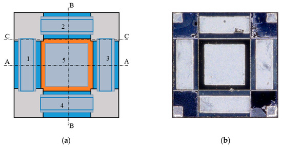

Figure 3.
TL-PSD chip—the A–A and B–B cross-section, according to Figure 2.

Figure 4.
TL-PSD chip—the C–C cross-section, according to Figure 2.

Table 1.
Schematic diagram of the layers in the mesa structure: their doping concentration, material composition, and thickness.
The photographs in Figure 5 present the hermetically sealed detector package (Figure 5a); its inner parts (Figure 5b) with the TL-PSD dice, which is flip-chip indium bump bonded to the chip carrier, on the cooler cold finger, where the cooler is soldered to a TO8 header; and the detector shortly connected to the electronics package (Figure 5c).
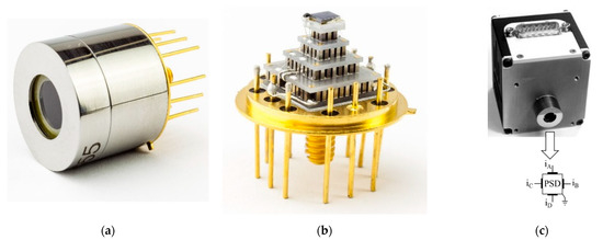
Figure 5.
Detector package (adapted with permission from Ref. [20]; copyright: 2022, SPIE): (a) the hermetic housing of the TL-PSD chip; (b) the TL-PSD chip on the four-stage Peltier cooler cold finger; (c) the TL-PSD detector integrated with the electronics package, and a spatial orientation of the cathode electrodes of the signal channels A, B, C, and D is also shown.
3. Dark Current Sources
Unfortunately, the radiative generation from the 300 K background is negligible compared to the non-radiative G-R components in this device. The dark current is suppressed with cooling, and the reverse bias further reduces the carrier concentrations below their thermal equilibrium levels thanks to a phenomenon specific to infrared narrow-gap semiconductor detectors—suppression of the Auger generation by extraction and exclusion of electric charge carriers with the reverse bias [23].
The dark current sources relevant to this detector are as follows [4] (pp. 247–260), [24] (pp. 82–86):
- Diffusion currents from the quasi-neutral (neutral) regions, mainly from the depleted in carriers but still neutral absorber volume, with their thermal G-R components:
- ○
- Auger 7 and Auger 1; in HgCdTe, the former dominates over the latter if the concentration of holes is more than about 10 times greater than that of electrons [24] (pp. 34, 136, 137), [25] (pp. 83–85);
- ○
- Shockley–Read–Hall (SRH);
- Currents from the space-charge (depletion) regions around (metallurgical) junctions:
- ○
- SRH (thermal G-R current in the space-charge region [26]);
- ○
- Trap-assisted tunneling (TAT) [27,28], with nearly linear dependence on reverse bias voltage < 1 V;
- ○
- Band-to-band tunneling (BTB), with voltage-dependence much stronger than linear;
- Possible components associated with injection to the absorber from the contact regions, mainly over the P+ barrier;
- Surface generation: SRH, tunneling, and conduction channels:
- ○
- at the edge of the mesa;
- ○
- along dislocations intercepting the junctions [29,30], i.e., reaching the space-charge regions in the absorber interfaces;
- Photoelectric gain mechanisms, affecting the dark current, noise, and responsivity but not the detectivity (sensitivity) of the detector [31,32];
- Internal radiative G-R is not important due to the photon recycling [33].
4. Noise Sources
The detector current fluctuates and so generates noise. Four types of noise are of importance in semiconductors [34]:
- Thermal (Johnson) noise and shot noise, with a constant (white) spectral density within the noise equivalent bandwidth;
- Random telegraph noise—a noise type that presents as a binary fluctuation in dark current, with a Lorentzian-shaped noise spectral density;
- 1/f noise, with the inverse dependence of the noise spectral power on frequency:
Scientists agree that 1/f noise in semiconductor devices is caused by fluctuations in electrical conductivity but differ on whether carrier concentration fluctuations [35] (pp. 207–228) or carrier mobility fluctuations [34], or both [36,37,38,39], are the cause.
The first paper on 1/f noise in HgCdTe photodiodes was published by Tobin et al. [40] in 1980. The authors found the 1/f noise to be proportional to the surface generation and surface leakage current of implanted n+-p MWIR HgCdTe photodiodes for a wide range of operating temperatures, from cryogenic with domination of the surface generation and surface leakage to higher temperatures, where the diffusion dark currents prevailed. The coefficient of proportionality, α, is often referred to as the Tobin coefficient:
where i is the detector overall current or one of its components, Td is the detector operating temperature, and Vb is the detector bias voltage. According to Tobin et al., the surface generation and surface leakage could be modulated by fluctuations in the surface potential, thus generating the 1/f noise. The authors were inspired by numerous works on 1/f noise studied in silicon and germanium filaments, p-n junctions [41], and MOS transistors, including McWhorter’s suggestion in 1953 that variations in the occupancy of the slow surface states caused conductivity fluctuations of semiconductor filaments and had a wide uniform spectrum of relaxation times corresponding to the 1/f noise [35] (pp. 207–228). Single-electron slow trapping de-trapping generates random telegraph noise [42]. In photodiodes, the slow trapping events mainly occur in passivation near the semiconductor surface or in the dislocations intercepting the junction, both in depletion regions.
Exemplary 1/f noise calculations for HgCdTe photodiodes were performed, based on McWhorter’s theory [29,43,44,45] or taking into account carrier mobility/scattering fluctuations [38,46]. The dislocations intercepting the junction were found to induce TAT and 1/f noise and are supposed to cause bandgap narrowing and getter impurities that can act as active trap centers [30,32,38,42,46,47,48].
In 2019, the new, more demanding standard was introduced by Teledyne—the MWIR and LWIR HgCdTe reverse biased photodiodes with fully depleted absorbers and close to the 300 K background limited performance [49]. In the fully depleted absorber, dislocations can be inactivated (“frozen”) because of lack of carriers throughout the absorber, even at the highest reported [49] operating temperature of 250 K, as they have been depleted and inactivated so far using cryogenic cooling. Then, the 1/f noise can be greatly reduced, providing the heteropassivation is applied by interdiffusion between the HgCdTe and the CdTe passivation layer during the high-temperature annealing. High-temperature annealing was also found to inactivate defects and dislocations in the active volume of the detector [47].
Another way to avoid or significantly reduce the 1/f noise is to minimize the depletion area using photodiodes optimized for 0 V bias or biased barrier devices, such as nBn [50,51].
5. Parameters of the Detector’s Equivalent Circuit
The equivalent circuits treat the TL-PSD like a four-way output current divider with four resistances. Their values can be approximated using the formulas written in Figure 6. The least error of such approximation is obtained at the center position of the light spot, with the radiation distribution approximated by Dirac’s delta function. Figure 7 shows a piece of the equivalent circuit suited for the finite element analysis—two adjacent cells of an array consisting of n × n equal cells. Rp denotes the differential parallel resistance and Cp denotes the differential parallel capacitance of the photodiode at a given reverse bias. The Rsh series resistance is the square sheet resistance of the resistive layer, and Rs com is the common series resistance, which is approximately the series resistance of the photodiode excluding the resistive layer. Both models are limited to the small signal case for which the input radiation power and the photocurrent are within the detector linear operation range.
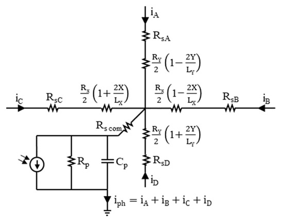
Figure 6.
TL-PSD equivalent circuit with the approximated formulas for the resistances of the photocurrent divider in the resistive layer, related to the light spot position (X, Y), where (0, 0) is in the center of the photosensitive area. The following values were determined at the detector operating temperature Td = 205 K and reverse bias Vb ≈ 0.16 V: Rp ≥ 100 Ω; Cp ≈ 1 nF; Rs com ≈ 0.6 Ω—the lead wire resistance; RX and RY may be assumed to equal Rsh = 5.5 Ω—the measured sheet resistance of the resistive layer; RsA = 8.9 Ω, RsB = 8.9 Ω, RsC = 9.0 Ω, and RsD = 9.2 Ω, with the main contribution of 8 Ω of the preamplifier input impedance, later calculated using Equation (9), and with minor contributions of contact resistance values from Table 2 and 0.6 Ω of the lead wire resistance.
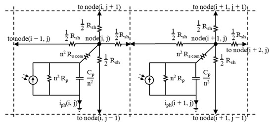
Figure 7.
Two cells of the TL-PSD equivalent circuit suited for the finite element analysis. The following values were determined at Td = 205 K and Vb ≈ 0.16 V: Rp ≥ 100 Ω; Cp ≈ 1 nF; Rsh = 5.5 Ω—the resistive layer sheet resistance; Rs com = 0.6 Ω—the lead wire resistance.
The linearity of the PSD signal versus the input radiation power as well as versus the light spot position and the resolution of the position measurement improve when the differential parallel impedance Rp‖Cp becomes much greater than the series impedance. The resistance of the photodiode was determined from DC measurement of its I-V characteristics, plotted in Figure 8, at the detector operating temperature Td = 205 K. It was important that the measurement was performed with all the A, B, C, and D outputs connected together. A significantly different shape of the characteristics, with an increased contribution of the series resistance, would be obtained if, for example, only one channel was connected to the ammeter and the other three were open.
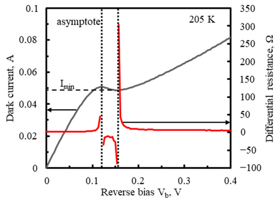
Figure 8.
Dark I−V characteristics of the TL−PSD photodiode with the 10–11 µm long wavelength cut-off at Td = 205 K.
At the reverse bias Vb outside the range of 0.1–0.2 V, the detector resistance dropped below <1 Ω and was dominated by the series resistance. With Vb increase to 0.12 V, the dark current became saturated due to the suppression of Auger generation, before the loss of Td stabilization by too much Joule heating could occur. The dark current slightly decreased with Vb in the range where the differential resistance was negative and then increased due to TAT, which narrowed the range of high differential resistances to a few millivolts of Vb. Even infinite differential resistance is theoretically possible, but a maximum of just over 100 Ω has been reached. This was due to the narrow Vb range with high differential resistances and the preamplifier input offset voltage, ranging from −0.5 to 0.5 mV [52].
The suppression of Auger generation with reverse bias is possible with low doping of the relatively thin HgCdTe absorber layer. However, in spite of its light p−-type doping (Table 1) and small thickness, we did not manage to suppress the electron concentration in the absorber to a negligible value. The minimal dark current at Vb ≈ 0.16 V occurred at the level corresponding to the Auger 1 rather than the Auger 7 diffusion current and was close to that predicted by “Rule 07” [53], a metric derived in 2007 for detectors limited by diffusion currents generated in a HgCdTe n-type absorber with extrinsic donor doping 1015 cm−3. Nevertheless, “Rule 07” has become a popular benchmark for state-of-the-art IR photodetectors based on other technologies, such as nBn and type II strained-layer superlattices.
The surface at the edge of this mesa structure insignificantly contributes to the dark current generation, due to the mesa transverse size being > 100 times greater than the carrier diffusion length. This was confirmed in dark current measurements of photodiodes of variable size from the same wafer. Nevertheless, the surface generation may significantly contribute to 1/f noise, as in [54].
The Rsh sheet resistance was checked as the resistance RC-B between the opposite cathode electrodes C and B and as the resistance RD-A between the opposite cathode electrodes D and A, when the anode electrode was electrically open. Figure 9 plots the differential resistances RC-B and RD-A and the currents versus the voltage put between the electrodes. The minimum RC-B and RD-A values were around 0 V and amounted to 5.5 Ω and 5.7 Ω, respectively, close to 5.5 Ω of the Rsh measured on the wafer before chip-processing. Assume an even distribution of the dark current Id between the cathode electrodes, Id/ch = 12 mA per one channel using 0.16 V of the reverse bias. During a normal operation of the PSD, when the photosignal varies linearly with the input radiation power, the amplitude of the total photocurrent iph does not exceed 4 mA, i.e., 1 mA per channel. The RC-B RC-B and RD-A values for ±16 mA, corresponding to the sum of ±12 mA of the dark current and ±4 mA of the photocurrent, are given in Table 2.
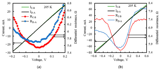
Figure 9.
Current and differential resistance versus voltage between the opposite cathode electrodes. The DC measurement at Td = 205 K with the photodiode electrically open. RC-B denotes resistance between the electrodes C and B, and RD-A denotes resistance between the electrodes D and A. These are resistances measured between the respective output pins outside the PSD hermetic package minus the resistance 1.2 Ω of two thin 25 µm diameter golden lead wires, connecting the output pins with the cathode electrodes. (a) Results shown in the bias voltage range −0.2 V to +0.2 V. (b) The same, with added results in the greater bias range.

Table 2.
Differential resistance between the opposite cathode electrodes at ±16 mA, based on the results shown in Figure 9, at Td = 205 K.
The resistance characteristics, exhibiting some nonlinearity and asymmetricity, and the observed differences between the RC-B, RD-A, and Rsh values indicate the possible contribution of the resistance of the metallization contact to the resistive layer. This is comparable to the resistance 0.6 Ω of the 25 µm diameter, 1 cm long gold lead wire and its compression bond used to connect the cathode electrode with the output pin. The sum of the metal–semiconductor contact resistance and that of the lead wire makes about 1 Ω of the detector series resistance at the output of each channel. It does not change with the light spot position and negatively affects the position error and the PSD linearity. Unfortunately, it was small compared to the 8 Ω for the input impedance of the integrating preamplifier, calculated later using Equation (9).
The inductance of the single lead wire can be assumed to be L = 13.3 nH, as the inductance of a straight gold wire 25 µm in diameter and 1 cm long [55,56]. For the applied integration times, which are time intervals τCDS of the correlated double sampling (CDS; Section 6), τCDS1 = 1 µs and τCDS2 = 0.5 µs, the 3 dB frequencies f of an integrating preamplifier transfer function are those of sinc(π τCDS f)—the Fourier transform of a rectangular pulse of τCDS width—f3dB1 = 0.44/τCDS1 = 440 kHz and f3dB2 = 0.44/τCDS2 = 880 kHz, respectively [57]. The impedance modules |ZL| of the wire introduced by the inductance L at f = f3dB1 and f = f3dB2 are |ZL1| = 2π × f3dB1 × L = 0.036 Ω and |ZL2| = 2π × f3dB2 × L = 0.072 Ω, negligible in comparison with 0.6 Ω of the wire resistance.
The Rs com common series resistance 0.6 Ω was introduced by the 25 µm diameter, 1 cm long gold lead wire and its compression bond used to connect the anode electrode with the output pin.
The parallel capacitance Cp scales proportionally to the photodiode photosensitive area and was only estimated from measurements of some reverse biased photodiodes, much smaller than the PSD photodiode and made of wafers similar to those used for this PSD. These were time response measurements using fast-decay laser pulses [22,58,59] as well as small-signal reflectance measurements with the vector network analyzer [60]. The Cp was estimated to be ca. 1 nF. As for Rp, such a value for Cp was possible due to suppression of the Auger generation with the reverse bias.
The photocurrent iph at the anode electrode (Figure 6 and Figure 7) is the sum of the photocurrents from all the four cathode electrodes. It can be found for a given input radiation spectral power Pinλ and a given spectral current responsivity Riλ of the detector using the relation: iph = Pinλ × Riλ. The low frequency Riλ of the PSD photodiode is shown in Figure 10. It was measured with a Fourier transform infrared spectrometer calibrated with a black-body radiation source with an accuracy of +/−20%. Short-wavelength radiation is largely filtered by the wide-gap cathode resistive layer, through which radiation enters the absorber, while the long-wavelength tail of the spectral characteristics is determined by the width and composition of the narrow-gap absorber.
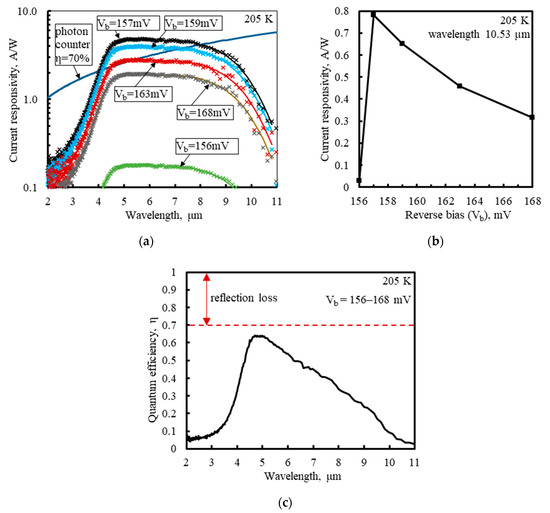
Figure 10.
Spectral responsivity of the PSD photodiode at Td = 205 K, from the photocurrent at the anode common contact, measured with the Fourier transform infrared spectrometer for the various reverse bias voltages Vb: (a) spectral characteristics (adapted with permission from Ref. [20]; copyright: 2022, SPIE); (b) rapid change in the responsivity with Vb around 0.16 V; (c) spectral quantum efficiency η = ηr × ηa.
Figure 10 reveals a strong dependence of the responsivity magnitude on Vb around 0.16 V, in the range of the high differential resistances, presented in Figure 8. The responsivity, strongly limited by the series resistance, was boosted with Vb between 156 mV and 157 mV and then gradually decreased as Vb increased. The rise in the responsivity was correlated with the sharp increase in the differential resistance of the detector, where the parallel resistance Rp was enhanced in relation to the series resistance. Moreover, at Vb in the range of 157 mV to 163 mV, the spectral responsivity exceeded that of the ideal photon counter with the quantum efficiency 70%, conforming to 100% − 70% = 30% of the radiation reflection losses in the detector, mainly at the air-GaAs interface of the chip substrate. This was the evidence of the photoelectric gain gph greater than unity. The gph value was estimated to equal ca. 1.7 for Vb = 159–160 mV, based on the following formula:
where h is Planck’s constant, c is the speed of light in a vacuum, is the photon energy, ηa is the absorption quantum efficiency deduced from fitting of modeling of the infrared absorption and transmission to the measured relative spectral response of the detector and room-temperature transmission of wafers with HgCdTe layers [61], ηr = 70% is the quantum efficiency related to the radiation reflection losses, and e is the charge of the electron.
6. Pulsed Radiation Measurement
The read-out circuitry (ROC) for the pulsed radiation measurements was realized in the form of a switched integrating transimpedance operational amplifier (op-amp) at each of the PSD’s four outputs. Figure 11 presents a general scheme of the ROC. The integrating op-amp consisted of the fast SiGe-based bipolar input ADA4896 op-amp integrated circuit chip [52], characterized by a low input current and voltage noise density, and the integrating capacitor Ci = 220 pF in the op-amp negative feedback loop, thus providing conversion of the integrated photocurrent to the output voltage across the Ci.
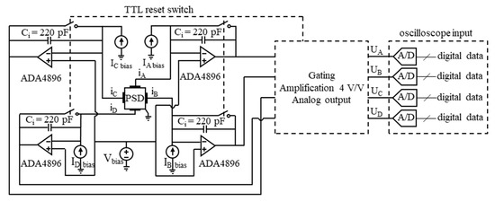
Figure 11.
General scheme of the read-out electronic circuit suited to the PSD photodetector, with the switched integrating preamplifiers, current sources compensating the reverse bias current individually for each channel, and one voltage source ensuring the constant reverse bias voltage for all the four channels. The output voltage was measured with a sampling analog-to-digital converter of the oscilloscope input.
The applied integration intervals were synchronized with 100 ns pulses of input radiation, emitted from the quantum cascade laser (QCL) with the 10 kHz repetition frequency. The timing of integration and sampling of the output voltage was controlled by a TTL-voltage compatible switching. This is illustrated in Figure 12, where Figure 12a shows an example output voltage waveform from one channel with a ca. 0.95 V photo-response to the 100 ns laser pulse and Figure 12b plots the output voltages from all four channels with the unlighted detector. Correlated double sampling (CDS) was applied. The first and second sample of each pair of the correlated samples of the output voltage were measured at time instants M1 and M2, respectively, when the reset switch (RS) was open. The first sample VM1 preceded the start of the radiation pulse and followed 0.5 μs after opening the RS at 0 ns. The second sample VM2 was taken well after the end of the radiation pulse, when all the photocurrent had been integrated. The voltage VM1 was subtracted from the voltage VM2. The measurement result was VM2−VM1, the CDS voltage. Next, the RS was closed for a time more than sufficient for discharge of the integrating capacitor. However, in the reset state (zeroing), the voltage across the capacitor settled at a level slightly different from zero. This zeroing offset could have been due to the op-amp input offset voltage, the flow of the uncompensated bias current through the RS, and charge injection during change of the RS state. The CDS dramatically reduced 1/f noise and the zeroing offset. The remaining output offset was due to the inaccurate compensation of the dark current, a small part of which flowed through the integrating capacitor.
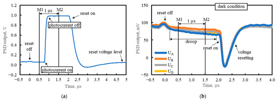
Figure 12.
Reset-and-integrate timing with the sampling time instants M1 and M2 shown: (a) example waveform of the output voltage from one channel, when the detector was lighted with the 100 ns laser pulse; (b) waveforms of the output voltages from all the channels, A, B, C, and D, when the detector was shielded from radiation.
This switched (also called box-car) integration of a signal improves the signal-to-noise ratio and is the preferred method for measuring weak pulsed radiation if an increase in measurement time is tolerated, such as when measuring pulse energy.
The input impedance of the ROC should be minimized so as not to unduly limit the photocurrent and the linearity of the PSD. This was achieved with the fast transimpedance op-amps, characterized by the relatively high open loop gain crossover frequency. The impedance mismatch was not significant here due to the limited bandwidth imposed by the applied value of the integration time τCDS.
The ROC should ensure the constant reverse bias voltage across the photodiode along with compensation of its bias (dark) current. The bias voltage should be within a relatively narrow range (Figure 8 and Figure 10), allowing sufficient depletion of carriers throughout the absorber, thus increasing the parallel impedance in relation to the series impedance so that the latter does not unreasonably limit the responsivity and linearity. The optimal bias voltage is then the same for all the channels. Its common regulation, as shown in Figure 11, was correct, as opposed to being separate for each channel.
Two detectors, each with a separate PSD chip from the same wafer, were assembled and integrated with the read-out electronics, forming two compact samples of PSD modules #1 and #2. The modules were attached to a heat-sink, which helped in the electronic stabilization of the detector operation temperature with a precision of 0.01 K. The output voltage was measured with an oscilloscope and mapped across the photosensitive area in a setup shown in Figure 13.
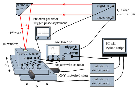
Figure 13.
Measurement setup for mapping a PSD photosignal across the photosensitive area.
The laser beam was focused with a parabolic mirror onto the photosensitive area of the PSD. A motorized X-Y stage, actuated by stepper motors, enabled scanning of the photosensitive area with the radiation spot. The measurement was controlled by a script written in Python programming language, installed on a computer (PC). The script collected and organized the sampling data of the output voltages UA, UB, UC, and UD from all four channels, obtained from the oscilloscope, and the data of the actual (X, Y) position of the radiation spot on the photosensitive area, received from the encoders of the stepper motors through their controllers. The actuation of the stepper motors was synchronized by the script with the time the PC received data from the oscilloscope and the encoders. Based on the gathered data, the script calculated the beam spot position (XPSD, YPSD) using Formulas (1) and (2), assigned it to the actual (X, Y) position data from the encoders, and presented the results in a graphical form.
An example waveform of the output voltage together with the input radiation power from the pulsed laser is presented in Figure 14. The radiation power was measured using another, uncooled photovoltaic detector type PVM-10.6-4×4, manufactured by VIGO Photonics S.A. (VIGO) (Ożarów Mazowiecki, Poland) [16,17,62], with the HgCdTe heterostructure consisting of multiple photovoltaic junctions connected in series that are distributed over a large photosensitive area of 4 mm × 4 mm. The PVM-10.6-4×4 detector is characterized by a large linearity range of the input radiation power and a low time constant of 1.0–1.5 ns, compared to the PSD presented herein.
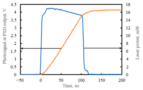
Figure 14.
Example waveforms: the input power of QCL radiation focused centrally on the PSD photosensitive area and the voltage signal from one of the PSD module outputs (adapted with permission from Ref. [20]; copyright: 2022, SPIE).
Based on the PSD equivalent circuit from Figure 7 and the values of its elements given therein, the time constant τPSD of the single-channel photoresponse can be approximated as follows:
where the detector is loaded by the integrating preamplifier input impedance Zin amp (Figure 11), which in fact is the resistance Rin amp for the considered frequencies > 100 kHz and can be calculated as follows:
where fc is the open loop gain crossover frequency of the ADA4896 op-amp used [52].
τPSD = [Rp‖(2 × Rscom + 0.5 × Rsh + Zin amp)] × Cp ≈ (2 × Rscom + 0.5 × Rsh + Rin amp) × Cp = (1.2 Ω + 0.5 × 5.5 Ω + 8 Ω) × 1 nF = 12 ns
Zin amp = Rin amp = (2πCifc)−1 = (2π × 220 pF × 90 MHz)−1 = 8 Ω
As was expected, neither the PSD nor the preamplifier input contributed significantly to the time of the PSD response to the 100 ns laser pulse (Figure 14).
Figure 15 demonstrates the characteristics of the signal from the PSD module output Uout = UA ≈ UB ≈ UC ≈ UD versus the energy of the radiation pulse of width tpulse = 100 ns and shows the linear operation limit equal to Uout_3%dev (tpulse = 100 ns) = 1.5 V at a 3% drop from the linear response. This corresponds to 0.54 nJ +/− 20% of the single-pulse energy at center illumination, where the signals from each channel are approximately equal, within +/−10% of the average. With deviation from center illumination, the pulse energy corresponding to the linear operation limit decreases to compensate for the increasing signal at the output with the highest voltage. The energy of the radiation pulse was measured by integrating the radiation power waveform obtained with the VIGO PVM-10.6-4×4 detector (Figure 14).
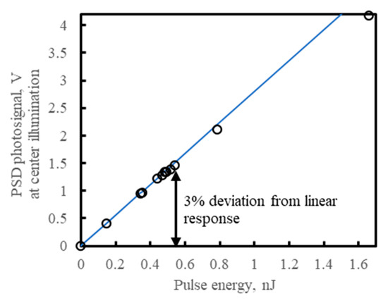
Figure 15.
Linearity characteristics—the PSD module output signal versus the energy of the single radiation pulse at center illumination, similar for the samples #1 and #2 of the PSD modules. Averaging no. 64. The QCL 100 ns pulses λ = 10.53 µm, the repetition rate 10 kHz, the Gaussian-like radiation spot of the 1/e2 diameter 240 µm, τCDS = 1 µs. The PSD photodiode was operated at Td = 205 K and the reverse bias Vb = 0.16 V.
It is optimal to operate within and not too far from the detector’s linear operation limit. Exceeding this limit could lower the differential impedance of the detector, the high value of which is crucial for good performance and stable operation. However, assume this PSD operates at the signal close to its linear operation limit, at a 3% drop from the linear response. Then, the photocurrent per channel Iph/ch_3%dev = 0.8 mA:
where Ku= 4 V/V is the gain of the output stage of the preamplifier (Figure 11). This photocurrent puts a significant voltage Us_3%dev = Iph/ch_3%dev × Rs = 10 mV across the series resistance Rs = 2 × Rscom + 0.5 × Rsh + Rin amp = 1.2 Ω + 0.5 × 5.5 Ω + 8 Ω = 12 Ω, from Equation (8), thus reducing by 10 mV the reverse bias voltage across the absorber and its interfaces. With a constant input radiation power, the photocurrent and photovoltage put across the series resistance of the corresponding channel increase with the distance of the radiation beam from the central illumination point. Thus, the reverse bias voltage, if set to optimal for central illumination, will be less than optimal the farther the radiation beam is moved away from the center. This also reduces the detector resistance in relation to the series resistance, lowers the responsivity and adds to the position nonlinearity.
Iph/ch_3%dev = Uout_3%dev × Ci/Ku/tpulse = 1.5 V × 220 pF/4/100 ns = 0.8 mA
The PSD area was scanned with 100 ns pulses of QCL radiation of λ = 10.53 µm and energy of 0.26 nJ, focused on a spot with a Gaussian-like profile (Figure 16) of the 1/e2 diameter 240 µm, with a repetition rate of 10 kHz. The PSD was operated at 205 K, and the reverse bias voltage Vb = 0.16 V, using τCDS = 1 µs. The resulting signal chromatic maps of the photosensitive area are presented in Figure 17, Figure 18 and Figure 19. The scan results in Figure 20 and Figure 21 were obtained under the same conditions.
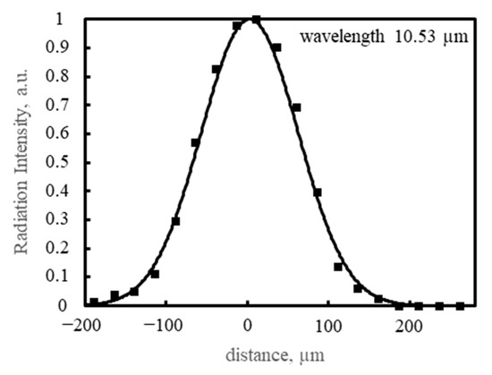
Figure 16.
Gaussian-like profile of a radiation spot emitted by the QCL. The 1/e2 diameter is 240 µm, measured with another Peltier-cooled HgCdTe photodiode with a small 30 µm × 30 µm photosensitive area, type PV-3TE-10.6-0.03 × 0.03, manufactured by VIGO Photonics S.A.
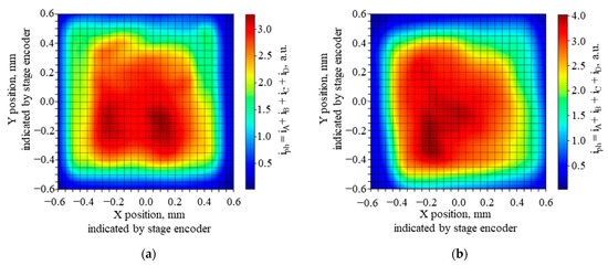
Figure 17.
Chromatic map of the sum of the signals from the channels A, B, C, and D for two samples of the PSD modules: (a) sample #1; (b) sample #2. Averaging no. 32. The maximal signal from a single channel was 1.2 V.

Figure 18.
Signal chromatic maps of the photosensitive area of the PSD module sample #1, taken from the individual channels separately. Averaging no. 32. The maximal signal 1.2 V.

Figure 19.
Signal chromatic maps of the photosensitive area of the PSD module sample #2, taken from the individual channels separately. Averaging no. 32. The maximal signal 1.2 V.
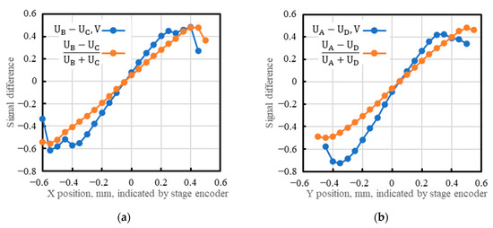
Figure 20.
Difference between signals from the opposite channels versus the radiation spot’s actual position: (a) UB − UC and (UB − UC)/(UB + UC) versus the position along the X axis; (b) UA − UD and (UA − UD)/(UA + UD) versus the position along the Y axis. (X = 0, Y = 0) is the middle of the photosensitive area.
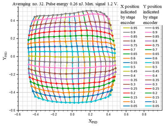
Figure 21.
PSD position error chart (adapted with permission from Ref. [20]; copyright: 2022, SPIE). Colored curves with the (XPSD, YPSD) points are assigned by color to the respective actual position (X, Y) values, given in two columns at the right. The encoders were zeroed at the corner of the area, so the central point is (X = 0.5, Y = 0.5), corresponding to (XPSD = 0, YPSD = 0). The PSD module sample #1.
In Figure 17, the map of the sum of all four outputs shows the periphery with > 30% of the signal attenuation, covering about half of the photosensitive area. This may be caused by the radiation spot extending partially outside the photosensitive area. In addition, other nonuniformities are clearly visible, also on subsequent maps in Figure 18 and Figure 19, taken for the signal from each PSD channel separately. No anti-etaloning solutions were applied, so etaloning due to radiation interferences in the wide-gap layers outside the absorber might contribute here. Inhomogeneities of the material layers, particularly the resistive layer, the cathode electrode metal–semiconductor contact, and the absorber and its interfaces may also play a role. Slightly more uniform maps were obtained for the next sample of the PSD module #2 (Figure 19).
Figure 20 plots linear scan results as the difference between the signals from the opposite channels versus the radiation spot’s actual position given by the encoders. Also shown is the interesting known linearization effect when the difference between the signals is divided by their sum. The linearization hides the nonuniformities visible in the plots of the simple difference (Figure 20a).
It was also interesting to measure a map of the difference, or error, between the (XPSD, YPSD) spot position determined from the PSD signals, using Equations (1) and (2), and the actual (X, Y) position given by the encoders. This is shown in Figure 21. The noise was merely visible due to the 32 averaging no. used. Nonlinearities are clearly visible, with barrel-like shapes characteristic of the tetra-lateral configuration of the cathode electrodes [13].
7. Noise Characterization
Figure 22 illustrates primary noise contributions for a typical connection of the PSD and the ROC. , , , and at the respective outputs are the roots of the sum of the signal variances from uncorrelated noise sources.
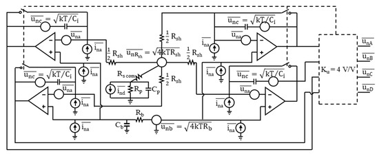
Figure 22.
Noise sources, rms, based on the connection diagram shown in Figure 11 and the detector’s equivalent circuit shown in Figure 7: and are the voltage and current, respectively, noise spectral densities of the preamplifier input; and are the noise voltage spectral densities of the bias voltage source and the resistive layer sheet resistance, respectively; is the noise voltage of the thermal fluctuations of the charge left on the integrating capacitor after opening an ideal switch.
The output noise is estimated under the following assumptions: the dark condition; the detector dark current is spread evenly between the four cathode electrodes A, B, C, and D, with the dark current per channel Id/ch = 12 mA at Vb = 0.16 V; and the voltage and current rms noises of the preamplifier input, and , respectively, are the same for all the preamplifiers used. Then, the same formula may be used for the total rms of the fluctuations , , , and of the charges QA, QB, QC, and QD, respectively, integrated during the CDS time interval τCDS on the capacitance Ci = 220 pF of the respective channels, and for the resulting noises , , , and :
where gph = 1.7 is estimated according to Equation (7); fk is the 1/f noise higher crossover (knee) frequency, below which the 1/f noise dominates; fk = 1 MHz is fit to the measured PSD photodiode noise current spectral density , shown in Figure 23, where ; the 1.1 exponent at the fk and the frequency variable f is a result of fit to the measured in the range, where the 1/f noise dominates; several fl values are assumed, where fl is the 1/f noise lower crossover frequency related to the time of the measurement [63], i.e., to τCDS; Td = 205 K; Te = 295 K is the operating temperature of the preamplifier; Zd = Rsh/2 + [(j2πfCp)−1‖Rp]; k is the Boltzmann constant; and e is the charge of the electron.
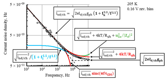
Figure 23.
Contributors to the noise current spectral density on the integrating capacitor of the PSD module. The measured dark current noise density per one channel is marked in black. Other respective highlighted expressions were calculated and taken from Equation (11). Components with sinc(πfτCDS) and fl factors are shown for τCDS = 1 µs, where fl is assumed to equal 1/(2πτCDS).
The high Cb=100 µF capacity connected in parallel with the Vb voltage source with the internal resistance Rb = 50 Ω limits the noise bandwidth at the output of the Vb voltage source to only 1/(4CbRb) = 50 Hz. This makes the noise of this source negligible, so it is not included in Equation (11).
The output noise voltage is calculated as follows:
where Ku= 4 V/V is the gain of the output stage of the preamplifier (Figure 11 and Figure 22) and is the vertical (voltage) rms noise of the oscilloscope for a given volt/div setting applied.
There could be some negative correlation between the respective noise contributions in the unA, unB, unC, and unD output noises originating from thermal (Johnson) noise of the resistive layer. This correlation is expected to increase with the PSD photodiode parallel impedance Zp = Rp‖(j2πfCp)−1. However, the contribution of the Johnson noise of the resistive layer is insignificant due to the limited noise bandwidth imposed by the CDS integrating interval τCDS through the sinc(πfτCDS) transfer function and because of domination of the huge 1/f noise of the PSD photodiode. This is shown in Figure 23, demonstrating several contributions to the noise current spectral density on the integrating capacitor. The black line fits points of half of the measured PSD photodiode noise current spectral density, , obtained with all the cathode outputs connected together, before integration of the PSD with electronics, and the red line provides the same noise with the added calculated Johnson noise current spectral density of the resistive layer. The contribution of the preamplifier input voltage noise spectral density , i.e., noise current spectral density, is insignificant too, for the same reason.
In addition, , , and are negligible.
The blue line in Figure 23 demonstrates strong limitation to the noise by the 1/f noise lower crossover frequency fl assumed to equal 1/(2πτCDS), as in [64]. Following [63], fl should be in inverse proportion to the measurement time, equal to τCDS here, and the value of fl can be obtained from measurements or a theory. The output noise voltage estimated by Equations (11) and (12) for the integration time τCDS = 1 µs and 0.5 µs and for the several values of fl is given in Figure 24.
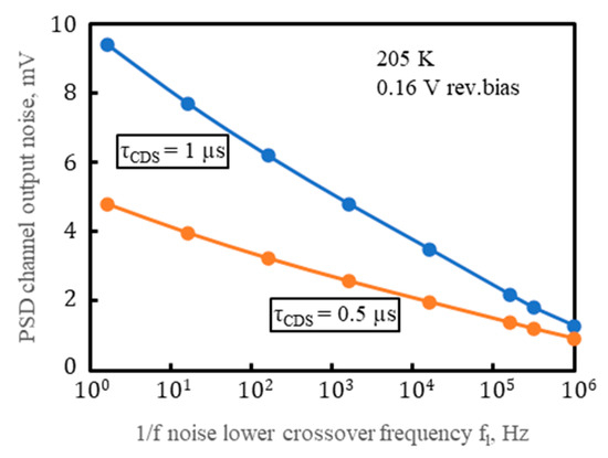
Figure 24.
The output noise voltage estimated by Equations (11) and (12) for the integration time τCDS = 1 µs and 0.5 µs and for the several values of the 1/f noise lower crossover frequency fl (adapted with permission from Ref. [20]; copyright: 2022, SPIE).
The output noise voltage measurement was carried out using the ROC and PSD connections from Figure 11 and a fast oscilloscope operated at 10 GigaSamples/second and 500 MHz bandwidth. The CDS technique described in Section 6 was used and no laser light was applied, so no photosignal was produced. Figure 25 is a histogram of the CDS voltages measured at τCDS = 1 μs and with the PSD operated at Vb = 0.16 V and Td = 205 K. The Gaussian-like distributions of the CDS voltage with its rms noises , , , and at the respective outputs were obtained. The measured values for the rms noise were 1.6 times greater than the output noise voltage estimated by Equations (11) and (12) for the same τCDS and conditions of PSD operation if fl = 1/(2π τCDS) was assumed, as in [64]. This is still reasonably good consistency between the measured and estimated noise values.
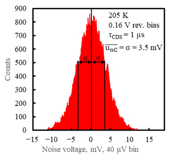
Figure 25.
Histogram of the CDS noise voltage unC, measured at the output C of the PSD module (adapted with permission from Ref. [20]; copyright: 2022, SPIE).
Finally, the measurement resolution of the (XPSD, YPSD) position was determined, and , based on:
- Equations (3) and (4);
- The measured noise of the output voltage;
- The output signals measured for the positions of the radiation spot where the maximum difference between the signals from the opposite cathode electrodes occurred, i.e., beyond the central area where a similar or better resolution was achieved.
The data are summarized in Table 3. The position resolution of 3–6 µm without averaging was obtained using the τCDS interval of 1 µs and 0.26 nJ 100 ns radiation pulses. However, the photocurrent was actually integrated just during the 100 ns radiation pulse. For the radiation pulse wider than the applied CDS interval, the photocurrent was integrated 10 times longer, over the entire interval τCDS = 1 µs, and the signal-to-noise ratio also increased 10 times. Thus, the position resolution of this PSD is 10 times better, i.e., 0.3–0.6 µm.

Table 3.
Output parameters of the PSD module, measured at the maximal difference between the signals from the opposite channels. The PSD module sample #1. No averaging. (adapted with permission from Ref. [20]; copyright: 2022, SPIE).
This position resolution could be further improved with modest averaging. Averaging improves signal-to-noise ratio N1/2 times, where N is the averaging number. Thus, the resolution is improved N1/2 times, too, according to Equations (3) and (4). The measurement time equal to τCDS = 1 µs plus a few microseconds for resetting would be increased N times then.
Using Equation (6), taking the dark current noise density per one channel = 4.1 × 10⁻⁹ A/Hz1/2 (Figure 23) and the dark current per one channel at the applied reverse bias Id/ch = 12 mA (Figure 8), we obtain the 1/f noise related Tobin coefficient:
which is a relatively small value compared to some other data from the last few years reported for HgCdTe devices at higher operating temperatures, e.g., for an MOCVD grown MWIR barrier detector at 205 K— = 2.7 × 10⁻⁴ [54] and for a liquid phase epitaxy (LPE) grown MWIR photodiode at 290 K— = 2–40 × 10−5 [65]. However, this may reflect not so much the quality of our photodiode as the larger share of the diffusion current in its dark current. Referring to diffusion-current-limited LPE MWIR and LWIR photodiodes at temperatures ≥ 200 K [66], ≈ 2 × 10⁻⁶ can be found.
However, dislocations intercepting the junction are likely to be a challenge, limiting the production yield of our relatively large 1 × 1 mm2 photodiodes. The probability of a dislocation intercepting the junction is proportional to the dislocation density and the junction area. We obtained the 1 mm × 1 mm photodiodes with yields a few times lower compared to devices with a smaller photosensitive area of 100 µm × 100 µm. The defective detectors had high dark currents and too-low resistances.
8. Summary and Conclusions
The lateral-effect position-sensitive Peltier-cooled LWIR detector was recently demonstrated [20] for the first time to the authors’ knowledge and described in more detail here. It was based on a modified PIN HgCdTe photodiode with a spectral sensitivity range of 3–11 μm, forming the tetra-lateral PSD with a photosensitive area of 1 × 1 mm2. The device was coupled to integrating preamplifiers and scanned with a focused radiation beam. It was capable of achieving a position resolution of 0.3–0.6 µm using a box-car integration time of 1 µs with correlated double sampling, which dramatically reduced the noise bandwidth and limited the contribution of the huge 1/f noise of this photodiode and the offsets of the output signal.
In order to improve the position linearity of this PSD, the cause of the observed nonuniformities in the signal maps should be further clarified, e.g., by comparison with maps obtained with a thermal radiation source. Anti-etaloning solutions should be considered. Inhomogeneities of the on-chip material layers, particularly the resistive layer, can be overcome by improving chip processing. However, the input impedance of integrating op-amps is comparable to and greater than the resistive layer sheet resistance, limiting the PSD performance, and differences between op-amp chips may also play a role. To avoid this, it is required to increase the impedance of the photodiode and the resistance of the resistive layer accordingly.
Due to the low yield and higher-than-expected thermal G-R, TAT, and resulting 1/f noise of this PSD, our technology should be investigated for improving dislocation density and surface passivation.
A 20-fold decrease in the dark current compared to the level exhibited by this PSD, possible with the fully depleted absorber, could significantly reduce the 1/f noise. Another way to avoid or lessen the 1/f noise is to minimize the depletion volume, e.g., with 0 V biased inter-band cascade infrared photodetectors based on InAs/InAsSb superlattices [50] or biased barrier devices, such as nBn made of HgCdTe [51], both optimized for suitably high resistance and fast response.
Resetting the integrating capacitor extends the time between position measurements to a few microseconds. With sufficiently low noise, non-integrating op-amps can be used that do not require resetting between measurements, allowing full use of the small time constant of this PSD, provided that the lead wire inductance is lowered according to the increased operating frequency.
Author Contributions
Conceptualization, J.P. (Jarosław Pawluczyk) and J.P. (Józef Piotrowski); Methodology, J.P. (Jarosław Pawluczyk) and M.Ż.; Validation, J.P. (Jarosław Pawluczyk), M.Ż. and J.P. (Józef Piotrowski); Formal analysis, J.P. (Jarosław Pawluczyk); Investigation, J.P. (Jarosław Pawluczyk) and M.Ż.; Resources, J.P. (Jarosław Pawluczyk) and M.Ż.; Data curation, J.P. (Jarosław Pawluczyk); Writing—original draft, J.P. (Jarosław Pawluczyk); Writing–review & editing, J.P. (Jarosław Pawluczyk), M.Ż. and J.P. (Józef Piotrowski); Visualization, J.P. (Jarosław Pawluczyk); Supervision, J.P. (Jarosław Pawluczyk) and J.P. (Józef Piotrowski). All authors have read and agreed to the published version of the manuscript.
Funding
This study has been supported by contract between VIGO Photonics S.A. in Poland and ASML Netherlands B.V.
Data Availability Statement
Data available within the article.
Acknowledgments
The authors appreciate helpful regular discussions with Roel Pouls and Wim van der Zande during the development of the device and help from Anton Montagne at the electronics design beginning from its concept and preliminary simulations.
Conflicts of Interest
The device was made and tested using the proprietary technology of VIGO Photonics S.A. in Poland. The authors declare no conflict of interest.
References
- Related Documents|Two-Dimensional PSDs|Hamamatsu Photonics. Available online: https://www.hamamatsu.com/eu/en/product/optical-sensors/distance-position-sensor/psd/two-dimensional-psd/related_documents.html (accessed on 17 March 2023).
- Chrzanowski, K.; Rogalski, A. Infrared Devices and Techniques (Revision). Metrol. Meas. Syst. 2014, 10, 565–618. [Google Scholar]
- Applications. Available online: https://vigophotonics.com/knowledge-base/applications/ (accessed on 17 March 2023).
- Rogalski, A. Infrared and Terahertz Detectors, 3rd ed.; CRC Press: Boca Raton, FL, USA; Taylor & Francis Group: Boca Raton, FL, USA, 2019; ISBN 978-1-138-19800-5. [Google Scholar]
- Calibrated Thermal Position & Power Sensors. Available online: https://www.thorlabs.com/newgrouppage9.cfm?objectgroup_id=13545 (accessed on 27 March 2023).
- Wolfshagen, R.; Smith, E.P.G.; Beuville, E.J.; Wilcox, M.; Venzor, G.M.; Peterson, J.M.; Reddy, M.; Wehner, J.G.A.; Ramirez, A.M.; Johnson, S.M.; et al. HgCdTe Position Sensitive Detector (PSD) Development. In Infrared Technology and Applications XXXVI; Andresen, B.F., Fulop, G.F., Norton, P.R., Eds.; SPIE: Orlando, FL, USA, 2010; Volume 7660, p. 76600H. [Google Scholar]
- Andersson, H. Position Sensitive Detectors—Device Technology and Applications in Spectroscopy. Ph.D. Thesis, Mid Sweden University, Sundsvall, Sweden, 2008. [Google Scholar]
- Hu, C.; Wang, X.; Song, B. High-Performance Position-Sensitive Detector Based on the Lateral Photoelectrical Effect of Two-Dimensional Materials. Light Sci. Appl. 2020, 9, 88. [Google Scholar] [CrossRef] [PubMed]
- Mäkynen, A. Position-Sensitive Devices and Sensor Systems for Optical Tracking and Displacement Sensing Applications. Ph.D. Thesis, University of Oulu, Oulu, Finland, 2000. [Google Scholar]
- Schottky, W. On the Origins of Photoelectrons in Cu2O-Cu Photocells. Phys. Z 1930, 31, 913–925. [Google Scholar]
- Wallmark, J. A New Semiconductor Photocell Using Lateral Photoeffect. Proc. IRE 1957, 45, 474–483. [Google Scholar] [CrossRef]
- Lucovsky, G. Photoeffects in Nonuniformly Irradiated P-n Junctions. J. Appl. Phys. 1960, 31, 1088–1095. [Google Scholar] [CrossRef]
- Woltring, H.J. Single- and Dual-Axis Lateral Photodetectors of Rectangular Shape. IEEE Trans. Electron Devices 1975, 22, 581–590. [Google Scholar] [CrossRef]
- Petersson, G.P.; Lindholm, L.-E. Position Sensitive Light Detectors with High Linearity. IEEE J. Solid-State Circuits 1978, 13, 392–399. [Google Scholar] [CrossRef]
- Lampton, M.; Carlson, C.W. Low-distortion Resistive Anodes for Two-dimensional Position-sensitive MCP Systems. Rev. Sci. Instrum. 1979, 50, 1093–1097. [Google Scholar] [CrossRef]
- Detector Types PVM, PVMQ and PCQ in Catalog of Products of VIGO Photonics, S.A. Available online: https://vigophotonics.com/knowledge-base/files/ (accessed on 17 March 2023).
- Pawluczyk, J.; Sosna, A.; Wojnowski, D.; Koźniewski, A.; Romanis, M.; Gawron, W.; Piotrowski, J. Higher Operation Temperature Quadrant Photon Detectors of 2-11 µm Wavelength Radiation with Large Photosensitive Areas. In Technologies for Optical Countermeasures XIV; SPIE: Warsaw, Poland, 2017; Volume 10435, p. 1043505. [Google Scholar]
- Qiao, S.; Liu, J.; Fu, G.; Wang, S.; Ren, K.; Pan, C. Laser-Induced Photoresistance Effect in Si-Based Vertical Standing MoS2 Nanoplate Heterojunctions for Self-Powered High Performance Broadband Photodetection. J. Mater. Chem. C 2019, 7, 10642–10651. [Google Scholar] [CrossRef]
- Position Sensing Detectors. Available online: https://www.thorlabs.com/newgrouppage9.cfm?objectgroup_id=4400 (accessed on 27 March 2023).
- Pawluczyk, J.; Zbik, M.F.; Piotrowski, J. Peltier Cooled LWIR Lateral Effect Position Sensitive HgCdTe Photodetector. In Quantum Sensing and Nano Electronics and Photonics XVIII; Razeghi, M., Ed.; SPIE: San Francisco, CA, USA, 2022; Volume PC12009, p. PC1200906. [Google Scholar]
- Cui, S.; Soh, Y.C. Linearity Indices and Linearity Improvement of 2-D Tetralateral Position-Sensitive Detector. IEEE Trans. Electron Devices 2010, 57, 2310–2316. [Google Scholar] [CrossRef]
- Pawluczyk, J.; Piotrowski, J.; Pusz, W.; Koźniewski, A.; Orman, Z.; Gawron, W.; Piotrowski, A. Complex Behavior of Time Response of HgCdTe HOT Photodetectors. J. Electron. Mater. 2015, 44, 3163–3173. [Google Scholar] [CrossRef]
- Ashley, T.; Elliott, C.T.; White, A.M. Non-Equilibrium Devices for Infrared Detection. In Infrared Technology XI; Mollicone, R.A., Spiro, I.J., Eds.; SPIE: San Diego, CA, USA, 1985; Volume 0572, p. 123. [Google Scholar]
- Kinch, M.A. Fundamentals of Infrared Detector Materials; Tutorial Texts Series; SPIE Press: Bellingham, WA, USA, 2007; ISBN 978-0-8194-6731-7. [Google Scholar]
- Piotrowski, J.; Rogalski, A. High-Operating-Temperature Infrared Photodetectors; SPIE: Bellingham, WA, USA, 2007; ISBN 978-0-8194-6535-1. [Google Scholar]
- Sah, C.; Noyce, R.N.; Shockley, W. Carrier Generation and Recombination in P-N Junctions and P-N Junction Characteristics. Proc. IRE 1957, 45, 1228–1243. [Google Scholar] [CrossRef]
- Rosencher, E.; Mosser, V.; Vincent, G. Transient-Current Study of Field-Assisted Emission from Shallow Levels in Silicon. Phys. Rev. B 1984, 29, 1135–1147. [Google Scholar] [CrossRef]
- Jóźwikowski, K.; Kopytko, M.; Rogalski, A.; Jóźwikowska, A. Enhanced Numerical Analysis of Current-Voltage Characteristics of Long Wavelength Infrared n-on-p HgCdTe Photodiodes. J. Appl. Phys. 2010, 108, 074519. [Google Scholar] [CrossRef]
- Kinch, M.A.; Strong, R.L.; Schaake, C.A. 1/f Noise in HgCdTe Focal-Plane Arrays. J. Electron. Mater. 2013, 42, 3243–3251. [Google Scholar] [CrossRef]
- Jóźwikowski, K.; Jóźwikowska, A.; Kopytko, M.; Rogalski, A.; Jaroszewicz, L.R. Simplified Model of Dislocations as a SRH Recombination Channel in the HgCdTe Heterostructures. Infrared Phys. Technol. 2012, 55, 98–107. [Google Scholar] [CrossRef]
- Davis, A.P.; Elliott, C.T.; White, A.M. Current Gain in Photodiode Structures. Infrared Phys. 1991, 31, 575–577. [Google Scholar] [CrossRef]
- Jóźwikowski, K.; Jóźwikowska, A. Enhanced Numerical Modeling of HgCdTe Long Wavelength Infrared Radiation High Operating Temperature Non-Equilibrium P+ν(π)N+ Photodiodes. J. Electron. Mater. 2019, 48, 6030–6039. [Google Scholar] [CrossRef]
- Humphreys, R.G. Radiative Lifetime in Semiconductors for Infrared Detection. Infrared Phys. 1986, 26, 337–342. [Google Scholar] [CrossRef]
- Hooge, F.N. 1/f Noise Sources. IEEE Trans. Electron Devices 1994, 41, 1926–1935. [Google Scholar] [CrossRef]
- Burstein, E.; McWhorter, A.L.; Miller, P.H.; Stevenson, D.T.; Weisz, P.B. Semiconductor Surface Physics; University of Pennsylvania Press: Philadelphia, PA, USA, 1957; ISBN 978-0-8122-7113-3. [Google Scholar]
- Black, R.D.; Weissman, M.B.; Restle, P.J. 1/f Noise in Silicon Wafers. J. Appl. Phys. 1982, 53, 6280–6284. [Google Scholar] [CrossRef]
- Van der Ziel, A. Semiclassical Derivation of Handel’s Expression for the Hooge Parameter. J. Appl. Phys. 1988, 63, 2456–2457. [Google Scholar] [CrossRef]
- Jóźwikowski, K.; Jóźwikowska, A.; Martyniuk, A. Dislocations as a Noise Source in LWIR HgCdTe Photodiodes. J. Electron. Mater. 2016, 45, 4769–4781. [Google Scholar] [CrossRef]
- Gross; Sodini. 1/f Noise in MOSFETs with Ultrathin Gate Dielectrics. In Proceedings of the 1992 International Technical Digest on Electron Devices Meeting, San Francisco, CA, USA, 13–16 December 1992; IEEE: San Francisco, CA, USA, 1992; pp. 881–884. [Google Scholar]
- Tobin, S.P.; Iwasa, S.; Tredwell, T.J. 1/f Noise in (Hg, Cd)Te Photodiodes. IEEE Trans. Electron Devices 1980, 27, 43–48. [Google Scholar] [CrossRef]
- Hsu, S.T. Surface State Related 1f Noise in P-n Junctions. Solid-State Electron. 1970, 13, 843–855. [Google Scholar] [CrossRef]
- Lee, D.; Carmody, M.; Piquette, E.; Dreiske, P.; Chen, A.; Yulius, A.; Edwall, D.; Bhargava, S.; Zandian, M.; Tennant, W.E. High-Operating Temperature HgCdTe: A Vision for the Near Future. J. Electron. Mater. 2016, 45, 4587–4595. [Google Scholar] [CrossRef]
- Kinch, M.A.; Wan, C.-F.; Schaake, H.; Chandra, D. Universal 1/f Noise Model for Reverse Biased Diodes. Appl. Phys. Lett. 2009, 94, 193508. [Google Scholar] [CrossRef]
- Schiebel, R.A. A Model for 1/f Noise in Diffusion Current Based on Surface Recombination Velocity Fluctuations and Insulator Trapping. IEEE Trans. Electron Devices 1994, 41, 768–778. [Google Scholar] [CrossRef]
- Anderson, W.W.; Hoffman, H.J. Surface-tunneling-induced 1/f Noise in Hg1−xCdxTe Photodiodes. J. Vac. Sci. Technol. A 1983, 1, 1730–1734. [Google Scholar] [CrossRef]
- Jóźwikowski, K.; Piotrowski, J.; Jóźwikowska, A.; Kopytko, M.; Martyniuk, P.; Gawron, W.; Madejczyk, P.; Kowalewski, A.; Markowska, O.; Martyniuk, A.; et al. The Numerical–Experimental Enhanced Analysis of HOT MCT Barrier Infrared Detectors. J. Electron. Mater. 2017, 46, 5471–5478. [Google Scholar] [CrossRef]
- Baker, I.; Maxey, C.; Hipwood, L.; Weller, H.; Thorne, P. Developments in MOVPE HgCdTe Arrays for Passive and Active Infrared Imaging. In Electro-Optical Remote Sensing, Photonic Technologies, and Applications VI; SPIE: Edinburgh, UK, 2012; Volume 8542, p. 85421A. [Google Scholar]
- Baker, I.M.; Maxey, C.D. Summary of HgCdTe 2D Array Technology in the U.K. J. Electron. Mater. 2001, 30, 682–689. [Google Scholar] [CrossRef]
- Lee, D.; Dreiske, P.; Ellsworth, J.; Cottier, R.; Chen, A.; Tallaricao, S.; Yulius, A.; Carmody, M.; Piquette, E.; Zandian, M.; et al. Law 19: The Ultimate Photodiode Performance Metric. In Infrared Technology and Applications XLVI; SPIE: Online Only, 2020; Volume 11407, p. 114070X. [Google Scholar]
- Gawron, W.; Kubiszyn, Ł.; Michalczewski, K.; Manyk, T.; Piotrowski, J.; Martyniuk, P. The Performance of the ICIP Ga-Free Superlattice Longwave Infrared Photodetector for High Operating Temperature. Infrared Phys. Technol. 2023, 128, 104499. [Google Scholar] [CrossRef]
- Benyahia, D.; Martyniuk, P.; Kopytko, M.; Antoszewski, J.; Gawron, W.; Madejczyk, P.; Rutkowski, J.; Gu, R.; Faraone, L. NBn HgCdTe Infrared Detector with HgTe(HgCdTe)/CdTe SLs Barrier. Opt. Quantum Electron. 2016, 48, 215. [Google Scholar] [CrossRef]
- ADA4896-2 Datasheet and Product Info|Analog Devices. Available online: https://www.analog.com/en/products/ada4896-2.html (accessed on 12 December 2022).
- Tennant, W.E.; Lee, D.; Zandian, M.; Piquette, E.; Carmody, M. MBE HgCdTe Technology: A Very General Solution to IR Detection, Described by “Rule 07”, a Very Convenient Heuristic. J. Electron. Mater. 2008, 37, 1406–1410. [Google Scholar] [CrossRef]
- Ciura, Ł.; Kopytko, M.; Martyniuk, P. Low-Frequency Noise Limitations of InAsSb-, and HgCdTe-Based Infrared Detectors. Sens. Actuators Phys. 2020, 305, 111908. [Google Scholar] [CrossRef]
- Inductance of a Straight Wire: A Calculator. Available online: http://www.consultrsr.net/resources/eis/induct5.htm (accessed on 12 December 2022).
- Grover, F.W. Inductance Calculations: Working Formulas and Tables; Instrument Society of America: Research Triangle Park, NC, USA, 1981; ISBN 978-0-87664-557-4. [Google Scholar]
- IVC102|Buy TI Parts|TI.Com. Available online: https://www.ti.com/product/IVC102/part-details/IVC102U (accessed on 11 December 2022).
- Żbik, M.; Wieczorek, P.Z. Versatile Subnanosecond Laser Diode Driver. In Photonics Applications in Astronomy, Communications, Industry, and High-Energy Physics Experiments 2016; Romaniuk, R.S., Ed.; SPIE: Wilga, Poland, 2016; Volume 10031, p. 100311F. [Google Scholar]
- Żbik, M.; Wieczorek, P. Charge-Line Dual-FET High-Repetition-Rate Pulsed Laser Driver. Appl. Sci. 2019, 9, 1289. [Google Scholar] [CrossRef]
- Zbik, M.; Szatkowski, J.; Wiatr, W. Time-Domain Characterization of High-Speed Mid-Infrared Photodetectors Using a Laser-Based Non-Linear Vector Network Analyzer System. In Proceedings of the 23rd International Microwave and Radar Conference (MIKON), Warsaw, Poland, 5–7 October 2020; pp. 263–267. [Google Scholar]
- Hougen, C.A. Model for Infrared Absorption and Transmission of Liquid-phase Epitaxy HgCdTe. J. Appl. Phys. 1989, 66, 3763–3766. [Google Scholar] [CrossRef]
- Gawron, W.; Damięcki, A.; Koźniewski, A.; Martyniuk, P.; Stasiewicz, K.A.; Madejczyk, P.; Rutkowski, J. Multiple Long Wavelength Infrared MOCVD Grown HgCdTe Photodetectors for High Temperature Conditions. IEEE Sens. J. 2021, 21, 4509–4516. [Google Scholar] [CrossRef]
- Niemann, M.; Kantz, H.; Barkai, E. Fluctuations of 1/f Noise and the Low-Frequency Cutoff Paradox. Phys. Rev. Lett. 2013, 110, 140603. [Google Scholar] [CrossRef]
- Gordon, N.T. Thermo Electrically Cooled Focal Plane Arrays Based on MCT. In Infrared Technology and Applications XXXVI; Andresen, B.F., Fulop, G.F., Norton, P.R., Eds.; SPIE: Orlando, FL, USA, 2010; Volume 7660, p. 76602X. [Google Scholar]
- Guinedor, P.; Brunner, A.; Rubaldo, L.; Bauza, D.; Reimbold, G.; Billon-Lanfrey, D. Low-Frequency Noises and DLTS Studies in HgCdTe MWIR Photodiodes. J. Electron. Mater. 2019, 48, 6113–6117. [Google Scholar] [CrossRef]
- Hassis, W.; Gravrand, O.; Rothman, J.; Benahmed, S. Low-Frequency Noise Characteristics of HgCdTe Infrared Photodiodes Operating at High Temperatures. J. Electron. Mater. 2013, 42, 3288–3296. [Google Scholar] [CrossRef]
Disclaimer/Publisher’s Note: The statements, opinions and data contained in all publications are solely those of the individual author(s) and contributor(s) and not of MDPI and/or the editor(s). MDPI and/or the editor(s) disclaim responsibility for any injury to people or property resulting from any ideas, methods, instructions or products referred to in the content. |
© 2023 by the authors. Licensee MDPI, Basel, Switzerland. This article is an open access article distributed under the terms and conditions of the Creative Commons Attribution (CC BY) license (https://creativecommons.org/licenses/by/4.0/).