
An Energy-Efficient BJT-Based Temperature Sensor with ±0.8 °C (3σ) Inaccuracy from −50 to 150 °C


Abstract
1. Introduction
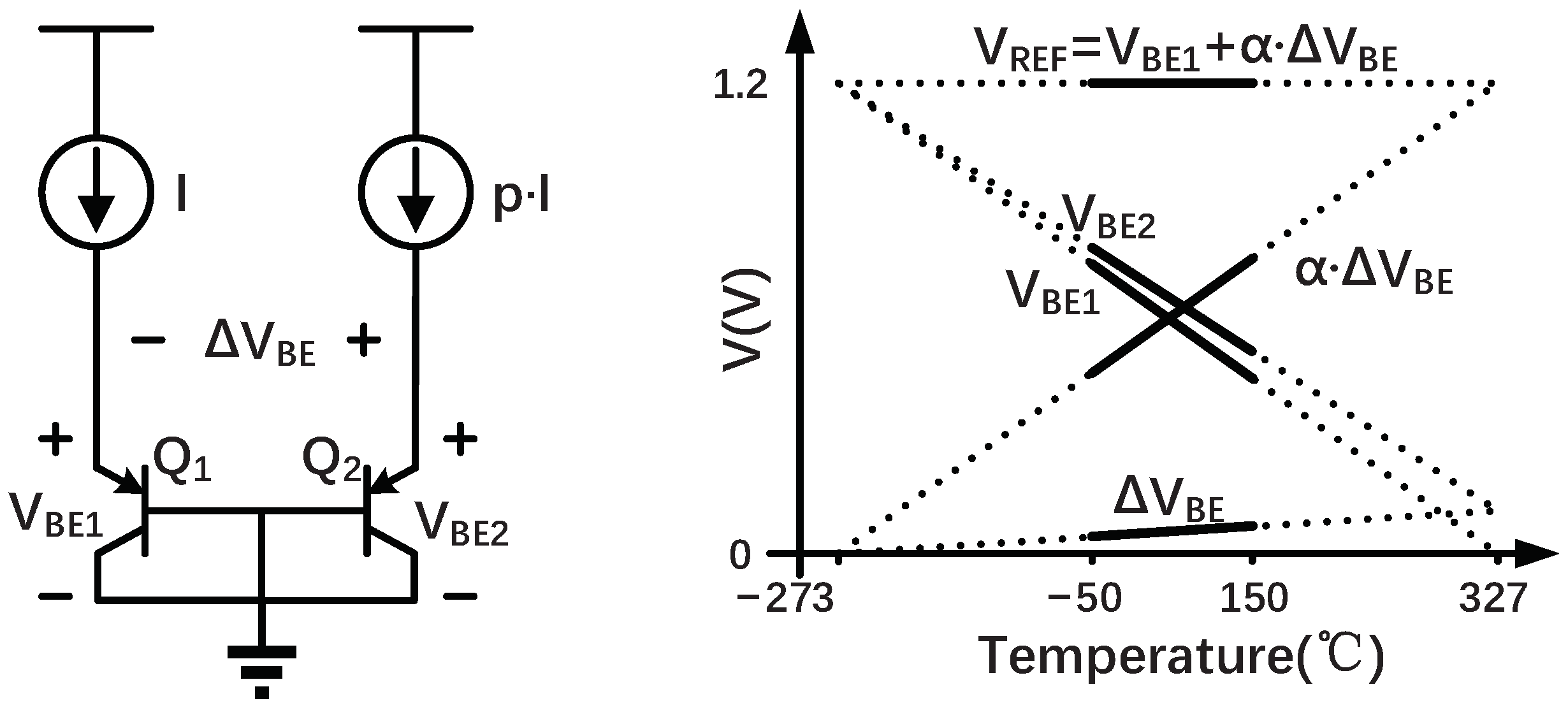
2. Operation Principle
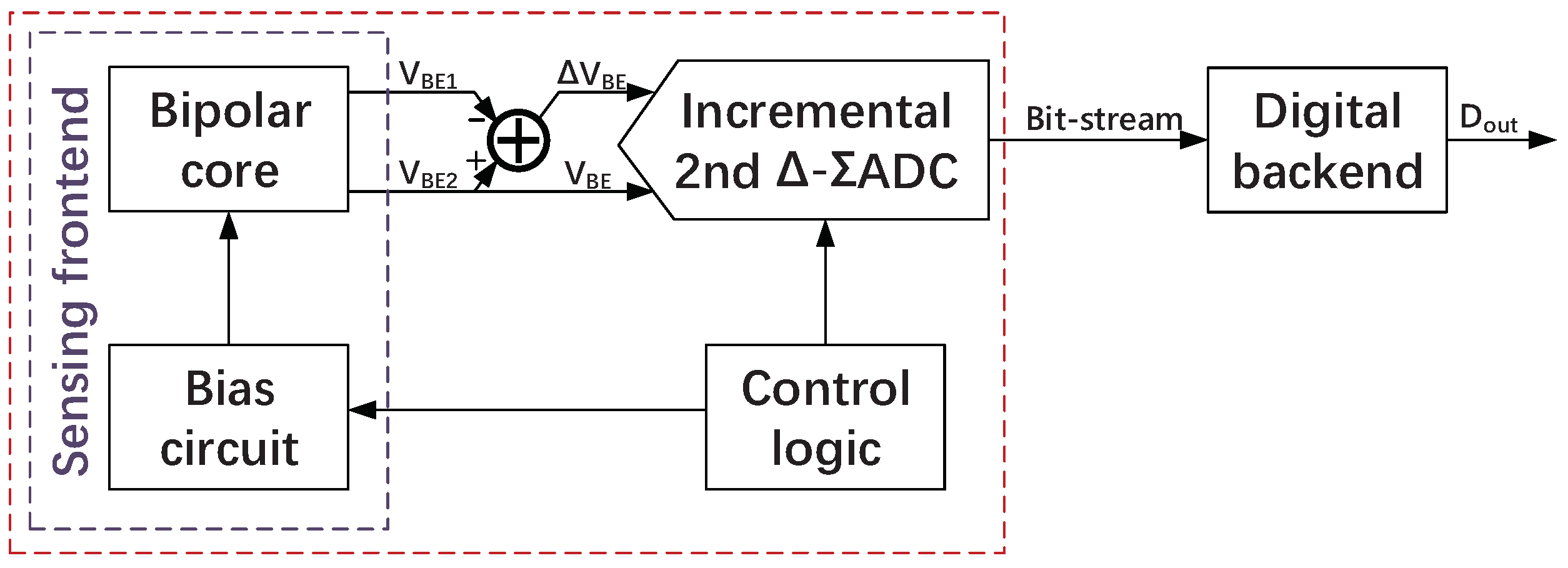
3. Sensing Front-End
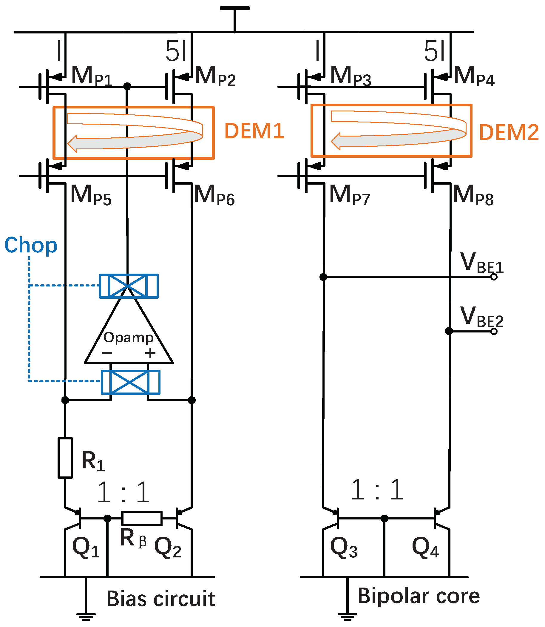
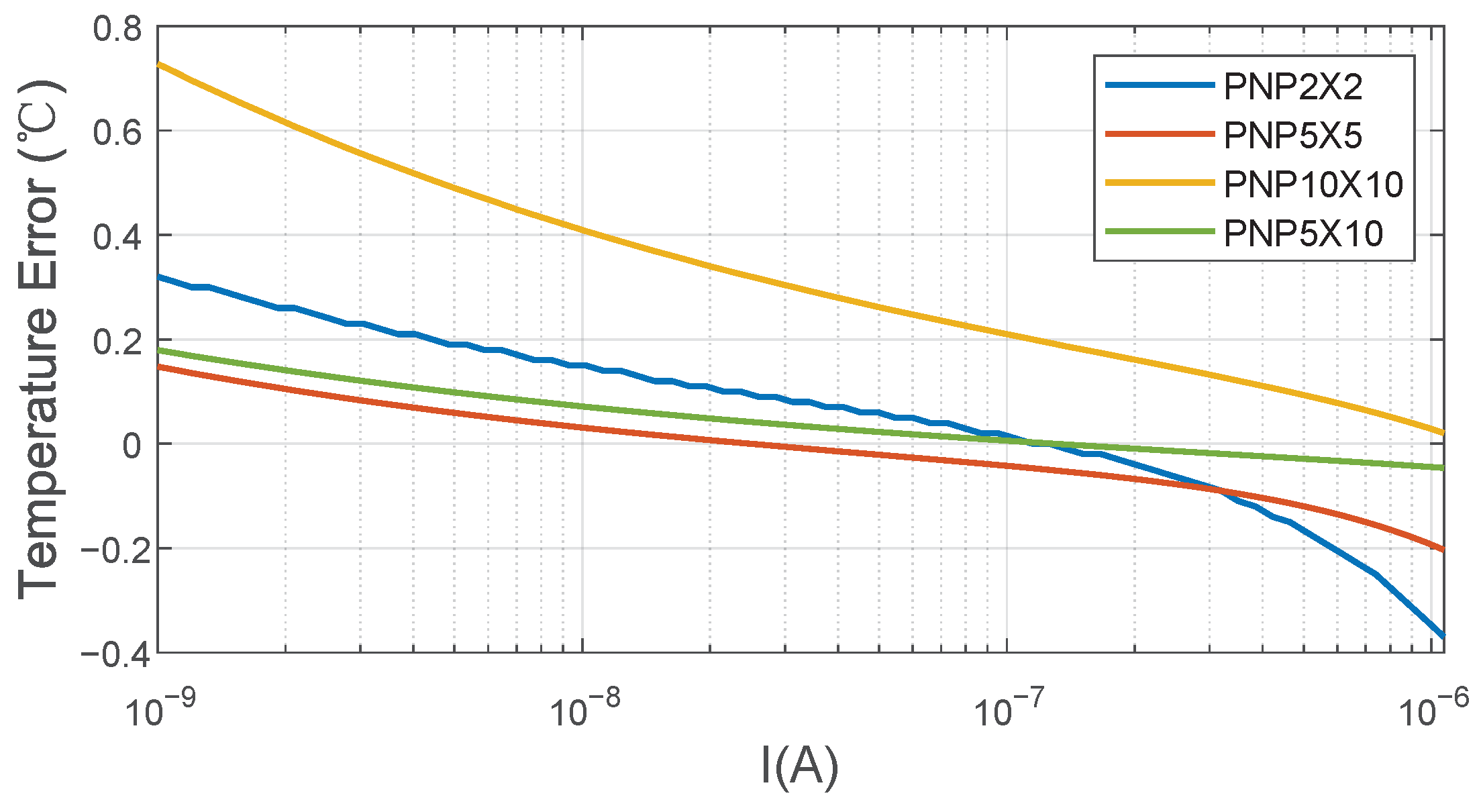
3.1. Effect of Current Gain
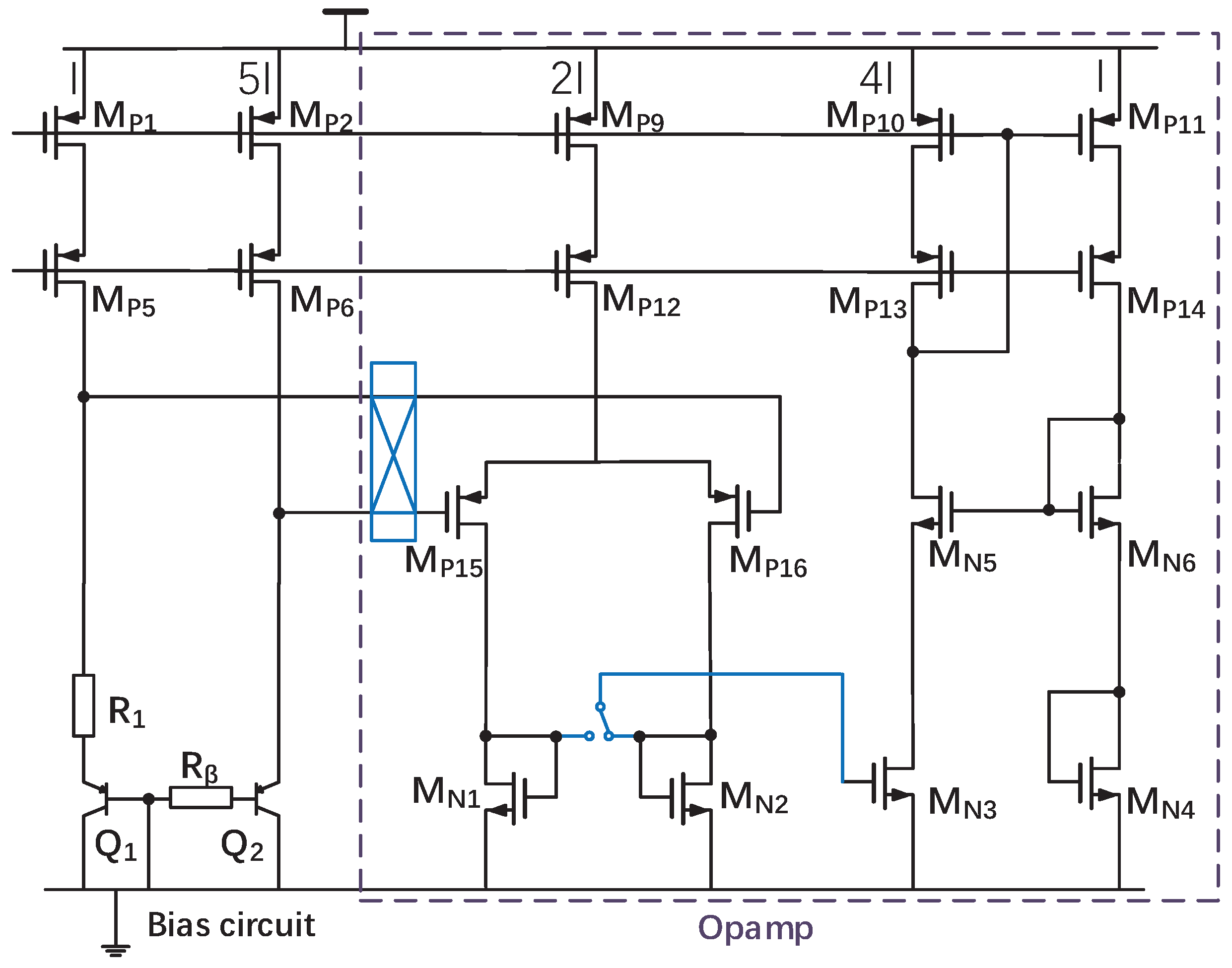
3.2. Opamp Topology
3.3. Precision Issues
4. Readout Circuit
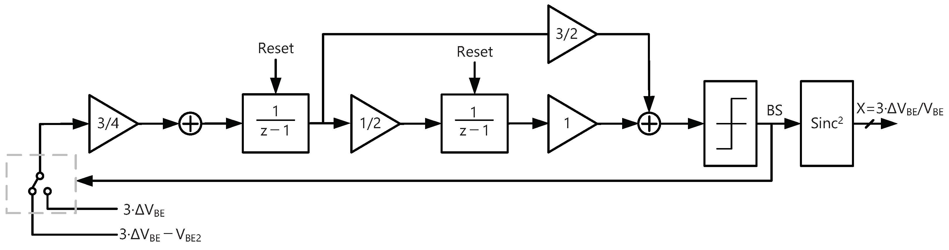
4.1. Incremental - ADC with Charge-Balancing Scheme
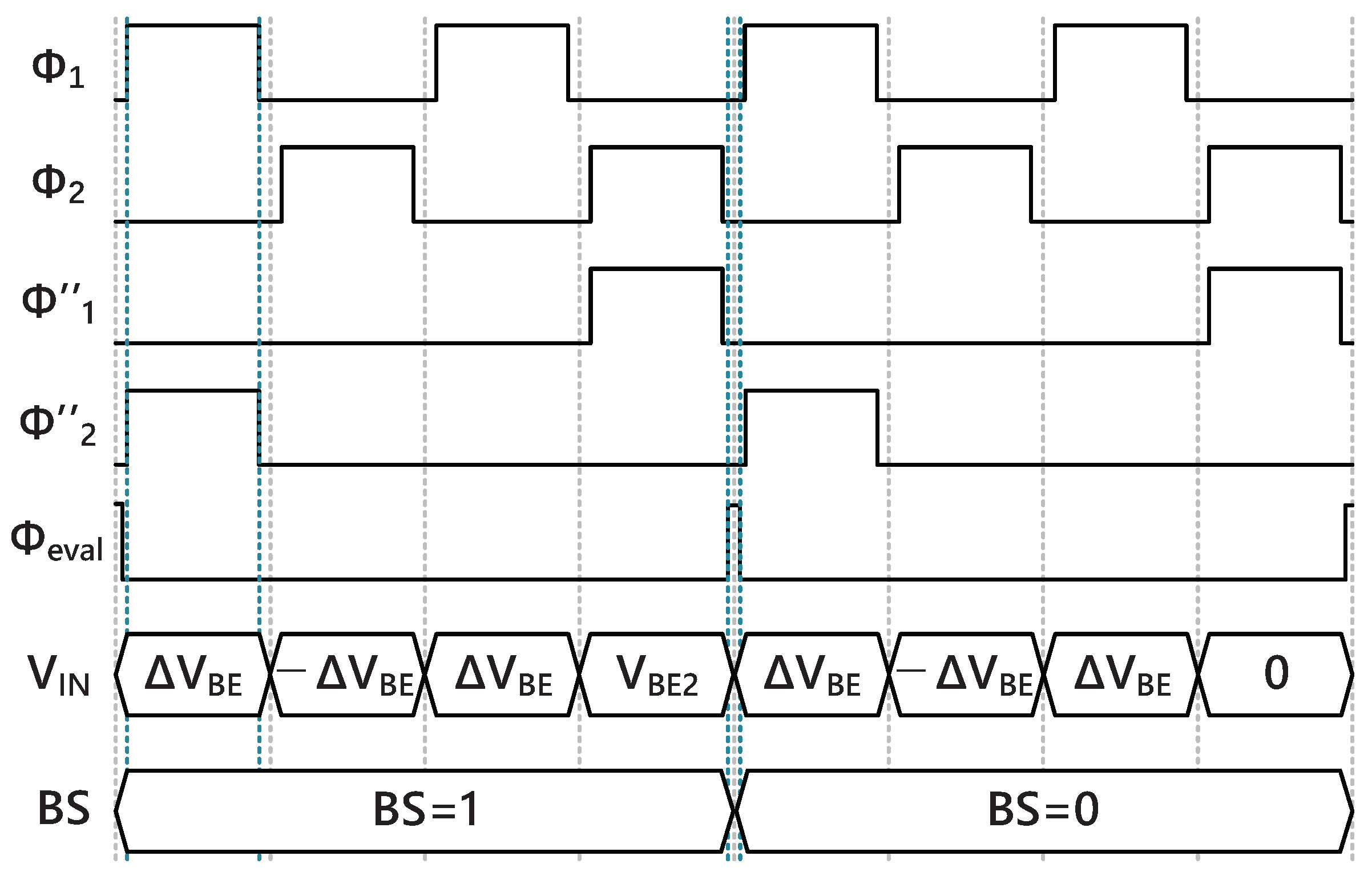
4.2. Sampling Scheme in the Incremental - ADC
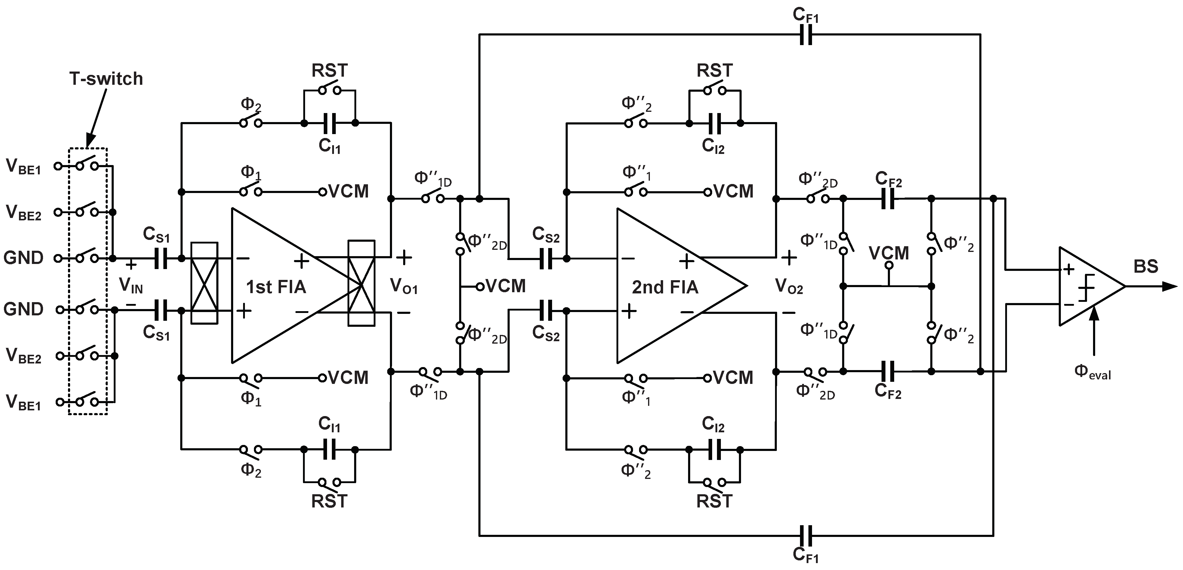
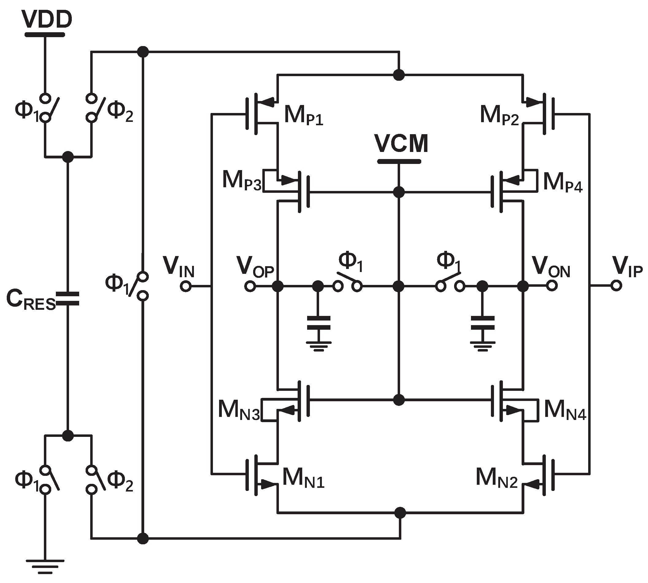
4.3. Cascoded FIA
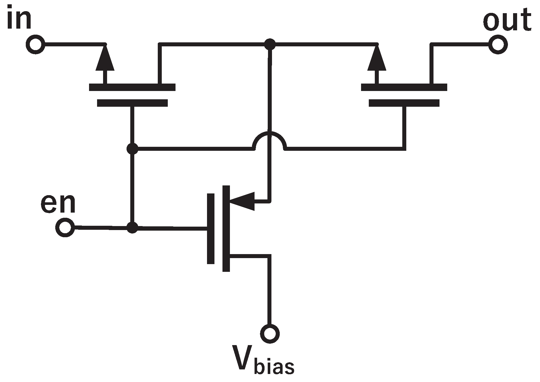
4.4. Switch Leakage
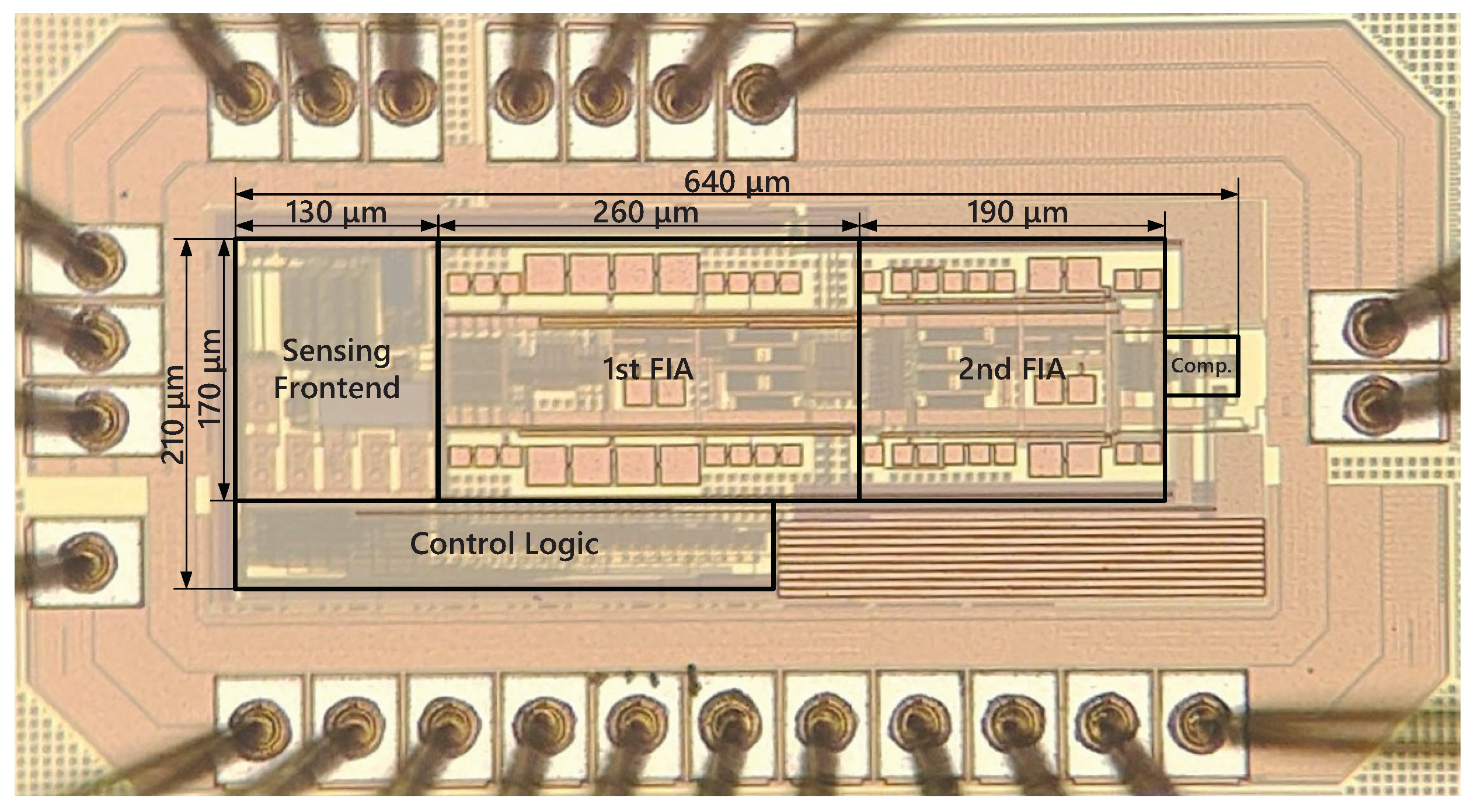
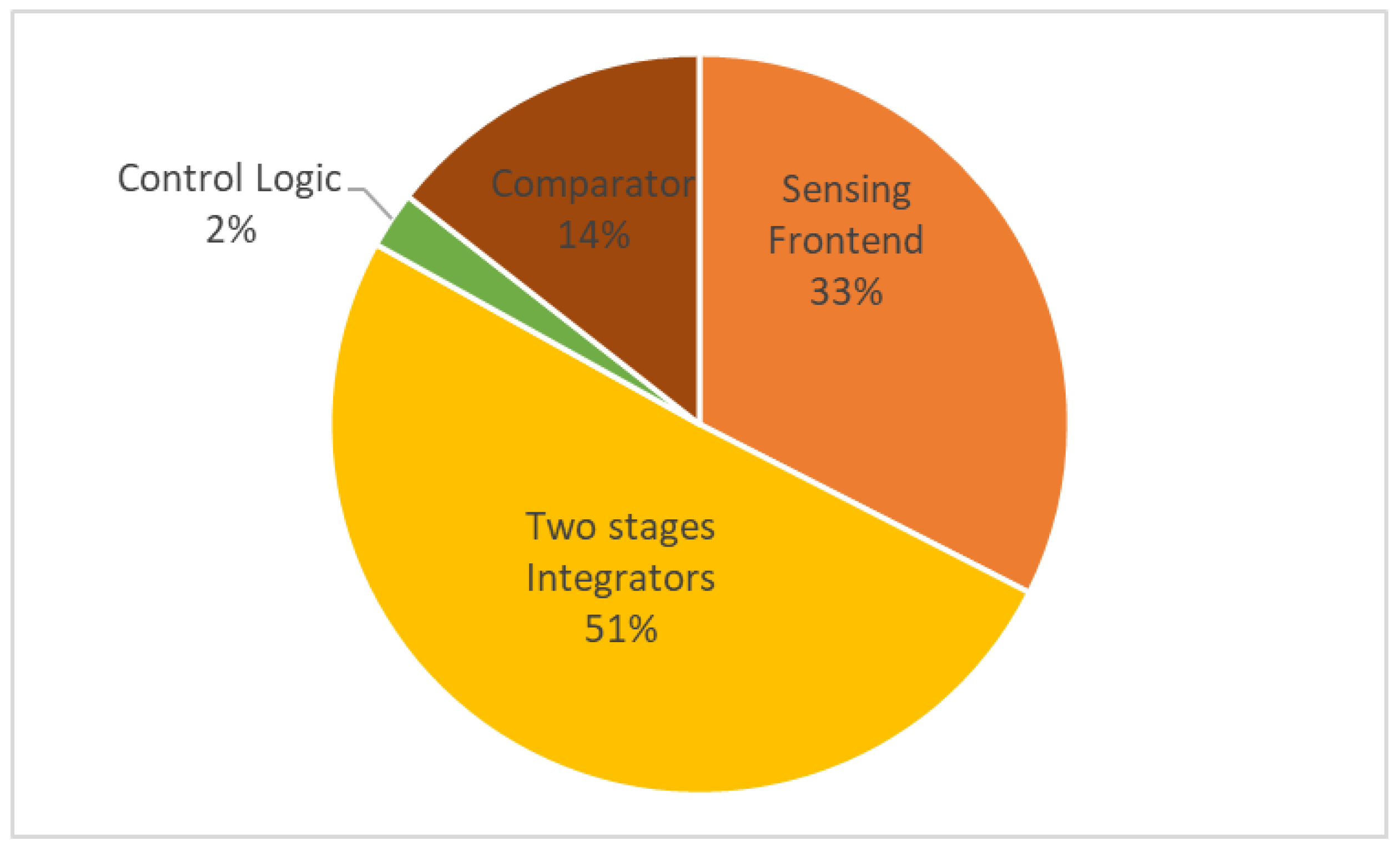
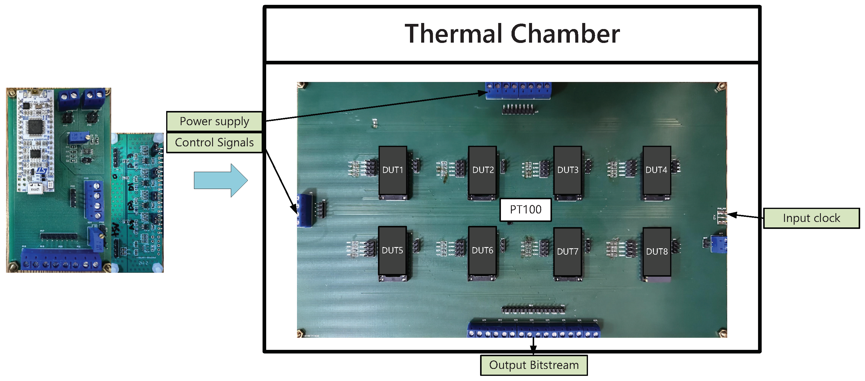
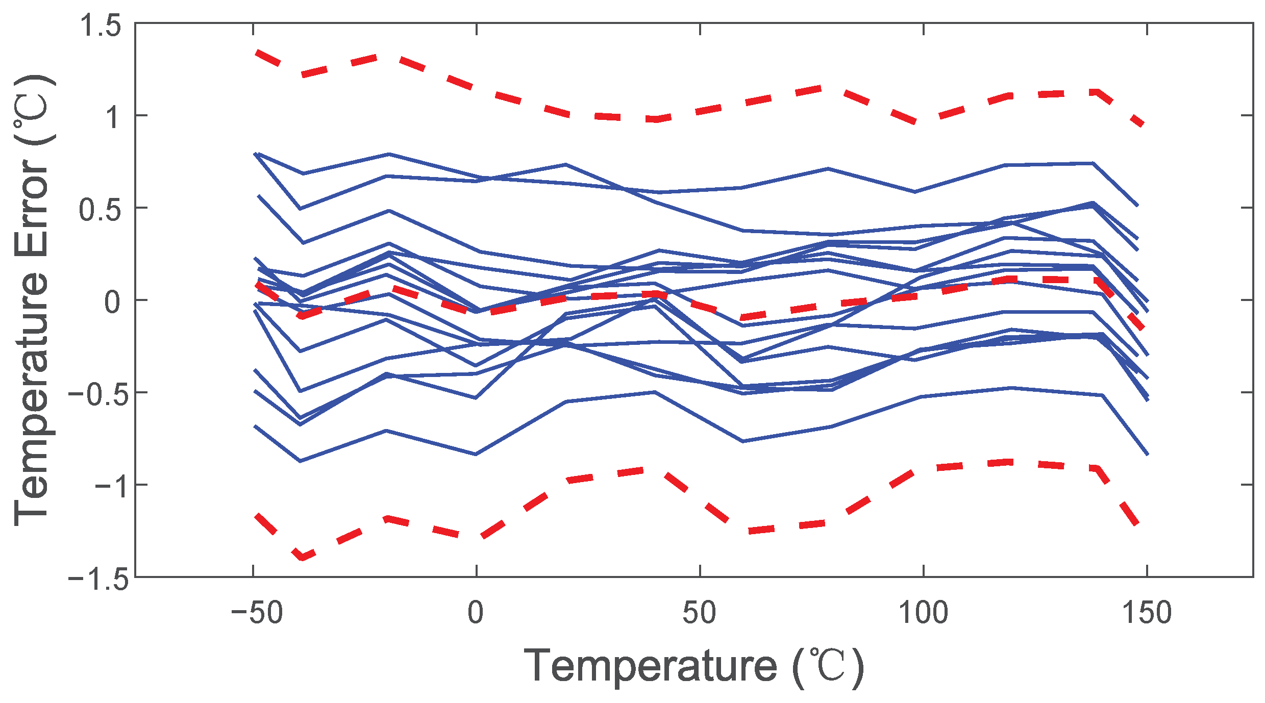
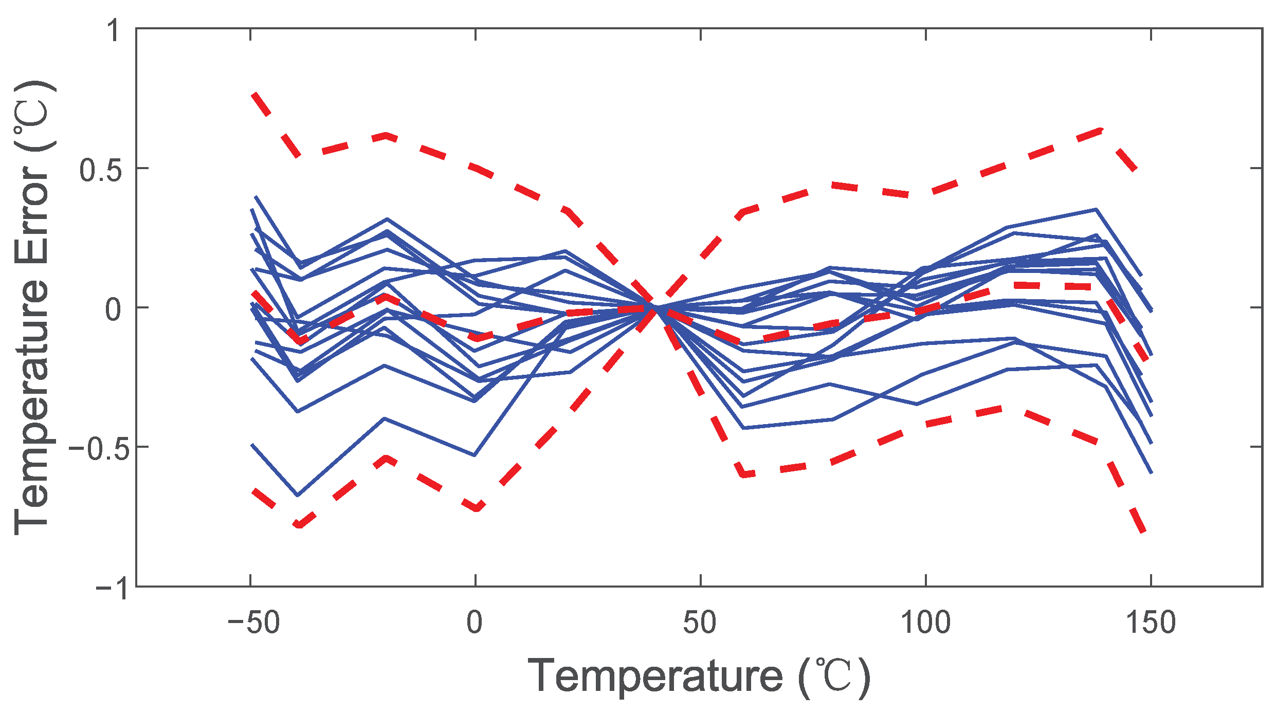
5. Exprimental Results
6. Conclusions
Author Contributions
Funding
Institutional Review Board Statement
Informed Consent Statement
Data Availability Statement
Conflicts of Interest
Abbreviations
| FIA | Floating-inverter-based dynamic amplifier |
| OTA | Operational transconductance amplifier |
| DEM | Dynamic element matching |
| BJT | Bipolar junction transistor |
| TD | Thermal diffusivity |
| HA-VCAL | Heater-assisted voltage calibration |
| ADC | Analog-to-digital converter |
| CTAT | Complementary to absolute temperature |
| PTAT | Proportional to absolute temperature |
| VCM | Common-mode voltage |
References
- Temperature Sensor Performance Survey. Available online: http://ei.ewi.tudelft.nl/docs/TSensor$_$survey.xls (accessed on 1 April 2022).
- Souri, K.; Makinwa, K.A.A. A 0.12 mm2 7.4 uW micropower temperature sensor with an inaccuracy of ±0.2 °C (3σ) from −30 °C to 125 °C. IEEE J.-Solid-State Circuits 2011, 46, 1693–1700. [Google Scholar] [CrossRef]
- Souri, K.; Chae, Y.; Makinwa, K.A.A. A CMOS Temperature Sensor with a Voltage-Calibrated Inaccuracy of ±0.15 °C (3σ) from −55 to 125 °C. IEEE J.-Solid-State Circuits 2012, 48, 292–301. [Google Scholar] [CrossRef]
- Yousefzadeh, B.; Shalmany, S.H.; Makinwa, K.A.A. A BJT-based temperature-to-digital converter with ±60 mK (3σ) inaccuracy from -55 °C to +125 °C in 0.16-um CMOS. IEEE J.-Solid-State Circuits 2017, 52, 1044–1052. [Google Scholar] [CrossRef]
- Wang, G.; Heidari, A.; Makinwa, K.A.A.; Meijer, G.C.M. An Accurate BJT-Based CMOS Temperature Sensor with Duty-Cycle-Modulated Output. IEEE Trans. Ind. Electron. 2017, 64, 1572–1580. [Google Scholar] [CrossRef]
- Pan, S.; Gürleyük, C.; Pimenta, M.F.; Makinwa, K.A.A. A 0.12 mm2 wien-bridge temperature sensor with 0.1 °C (3σ) inaccuracy from −40 °C to 180 °C. In Proceedings of the 2019 IEEE International Solid- State Circuits Conference- (ISSCC), San Francisco, CA, USA, 17–21 February 2019; pp. 184–186. [Google Scholar]
- Van Vroonhoven, C.P.L.; Makinwa, K.A.A. An SOI thermal-diffusivity-based temperature sensor with ±0.6 °C (3Σ) untrimmed inaccuracy from −70 °C to 170 °C. Sens. Actuators Phys. 2011, 188, 2887–2890. [Google Scholar]
- Van Vroonhoven, C.; D’Aquino, D.; Makinwa, K. A ±0.4 °C (3σ) 70 to 200 °C time-domain temperature sensor based on heat diffusion in Si and SiO2. In Proceedings of the 2012 IEEE International Solid-State Circuits Conference, San Francisco, CA, USA, 19–23 February 2012; pp. 204–206. [Google Scholar]
- Souri, K.; Souri, K.; Makinwa, K. A 40 μW CMOS temperature sensor with an inaccuracy of ±0.4 °C (3σ) from −55 °C to 200 °C. In Proceedings of the 2013 Proceedings of the ESSCIRC (ESSCIRC), Bucharest, Romania, 16–20 September 2013; pp. 221–224.
- Chuang, M.-C.; Tai, C.-L.; Hsu, Y.-C.; Roth, A.; Soenen, E. A temperature sensor with a 3 sigma inaccuracy of ±2 °C without trimming from −50 °C to 150 °C in a 16 nm FinFET process. In Proceedings of the ESSCIRC Conference 2015—41st European Solid-State Circuits Conference (ESSCIRC), Graz, Austria, 14–18 September 2015; pp. 271–274. [Google Scholar]
- Yousefzadeh, B.; Makinwa, K.A.A. A BJT-Based Temperature-to-Digital Converter with a ±0.25 °C (3σ)-Inaccuracy From −40 °C to +180 °C Using Heater-Assisted Voltage Calibration. IEEE J.-Solid-State Circuits 2019, 55, 369–377. [Google Scholar] [CrossRef]
- Pertijs, M.A.P.; Huijsing, J.H. Precision Temperature Sensors in CMOS Technology; Springer: Dordrecht, The Netherlands, 2006; pp. 51–58. [Google Scholar]
- Pertijs, M.A.P.; Makinwa, K.A.A.; Huijsing, J.H. A CMOS smart temperature sensor with a 3/spl sigma/ inaccuracy of /spl plusmn/0.1/spl deg/C from -55/spl deg/C to 125/spl deg/C. IEEE J.-Solid-State Circuits 2005, 40, 2805–2815. [Google Scholar] [CrossRef]
- Pertijs, M.; Huijsing, J. Bias Circuits. U.S. Patent 7 446 598 B2, 4 November 2008. [Google Scholar]
- Markus, J.; Silva, J.; Temes, G.C. Theory and applications of incremental /spl Delta//spl Sigma/ converters. IEEE Trans. Circuits Syst. I Regul. Pap. 2004, 51, 678–690. [Google Scholar] [CrossRef]
- Yücetaş, M.; Pulkkine, M.; Gronicz, J.; Halonen, K. A temperature sensor with (3σ) inaccuracy of +0.5/−0.75 °C and energy per conversion of 0.65 μJ using a 0.18 μm CMOS technology. In Proceedings of the 2013 NORCHIP, Vilnius, Lithuania, 11–12 November 2013; pp. 1–4. [Google Scholar]
- Tang, Z.; Fang, Y.; Yu, X.-P.; Shi, Z.; Tan, N. A CMOS Temperature Sensor With Versatile Readout Scheme and High Accuracy for Multi-Sensor Systems. IEEE Trans. Circuits Syst. I Regul. Pap. 2018, 65, 3821–3829. [Google Scholar] [CrossRef]
- Kumar, R.S.A.; Krishnapura, N.; Banerjee, P. Analysis and Design of a Discrete-Time Delta-Sigma Modulator Using a Cascoded Floating-Inverter-Based Dynamic Amplifier. IEEE J.-Solid-State Circuits 2022, 57, 3384–3395. [Google Scholar] [CrossRef]
- Tang, X.; Kasap, B.; Shen, L.; Yang, X.; Shi, W.; Sun, N. An Energy-Efficient Comparator with Dynamic Floating Inverter Pre-Amplifier. In Proceedings of the 2019 Symposium on VLSI Circuits, Kyoto, Japan, 9–14 June 2019; pp. C140–C141. [Google Scholar]
- Tang, X.; Yang, X.; Zhao, W.; Hsu, C.-K.; Liu, J.; Shen, L.; Mukherjee, A.; Shi, W.; Li, S.; Pan, D.Z.; et al. A 13.5-ENOB, 107-μW Noise-Shaping SAR ADC with PVT-Robust Closed-Loop Dynamic Amplifier. IEEE J.-Solid-State Circuits 2020, 55, 3248–3259. [Google Scholar] [CrossRef]
- Ishida, K.; Kanda, K.; Tamtrakarn, A.; Kawaguchi, H.; Sakurai, T. Managing leakage in charge-based analog circuits with low-V/sub TH/ transistors by analog T-switch (AT-Switch) and super cut-off CMOS. In Proceedings of the 2005 Symposium on VLSI Circuits, Kyoto, Japan, 16–18 June 2005; pp. 122–125. [Google Scholar]
- Pathrose, J.; Liu, C.; Chai, K.T.C.; Xu, Y.P. A Time-Domain Band-Gap Temperature Sensor in SOI CMOS for High-Temperature Applications. IEEE Trans. Circuits Syst. II Express Briefs 2015, 62, 436–440. [Google Scholar] [CrossRef]


| [9] | [10] | [17] | [22] | This Work | |
|---|---|---|---|---|---|
| Technology | 160 nm CMOS | 16 nm FinFET | 130 nm CMOS | 1 m CMOS | 180 nm CMOS |
| Area (mm) | 0.1 | 0.0126 | 0.29 | 0.41 | 0.13 |
| Temp. range (°C) | −55∼200 | −50∼150 | −40∼125 | 25∼225 | −50∼150 |
| Calibration | 1-point | 0-point | 1-point | 1-point | 1-point |
| Supply (V) | 1.8 | 1.8 | 2–3.6 | 4.5 | 1.8/3.3 |
| Power (W) | 39.6 | 1210 | 313.5 | 90 | 45.7 |
| Inaccuracy (°C) | ±0.4 (3) | ±2 (3) | ±0.47 (3) | ±1.6 | ±0.8 (3) |
| Relative inaccuracy (%) 1 | 0.31 | 2 | 0.57 | 1.6 | 0.8 |
| Resolution (°C) | 0.02 | 0.38 | 0.016 | 0.2 | 0.04 |
| Conversion rate (ms) | 4.2 | 0.27 | 5.12 | 100 | 10.24 |
| Energy/Conv. (nJ) | 150 | 330 | 1600 | 9000 | 468 |
Publisher’s Note: MDPI stays neutral with regard to jurisdictional claims in published maps and institutional affiliations. |
© 2022 by the authors. Licensee MDPI, Basel, Switzerland. This article is an open access article distributed under the terms and conditions of the Creative Commons Attribution (CC BY) license (https://creativecommons.org/licenses/by/4.0/).
Share and Cite
Qin, C.; Huang, Z.; Liu, Y.; Li, J.; Lin, L.; Tan, N.; Yu, X. An Energy-Efficient BJT-Based Temperature Sensor with ±0.8 °C (3σ) Inaccuracy from −50 to 150 °C. Sensors 2022, 22, 9381. https://doi.org/10.3390/s22239381
Qin C, Huang Z, Liu Y, Li J, Lin L, Tan N, Yu X. An Energy-Efficient BJT-Based Temperature Sensor with ±0.8 °C (3σ) Inaccuracy from −50 to 150 °C. Sensors. 2022; 22(23):9381. https://doi.org/10.3390/s22239381
Chicago/Turabian StyleQin, Chuyun, Zhenyan Huang, Yuyan Liu, Jiping Li, Ling Lin, Nianxiong Tan, and Xiaopeng Yu. 2022. "An Energy-Efficient BJT-Based Temperature Sensor with ±0.8 °C (3σ) Inaccuracy from −50 to 150 °C" Sensors 22, no. 23: 9381. https://doi.org/10.3390/s22239381
APA StyleQin, C., Huang, Z., Liu, Y., Li, J., Lin, L., Tan, N., & Yu, X. (2022). An Energy-Efficient BJT-Based Temperature Sensor with ±0.8 °C (3σ) Inaccuracy from −50 to 150 °C. Sensors, 22(23), 9381. https://doi.org/10.3390/s22239381