
A 2 MS/s Full Bandwidth Hall System with Low Offset Enabled by Randomized Spinning


Abstract
:1. Introduction
2. Error Model
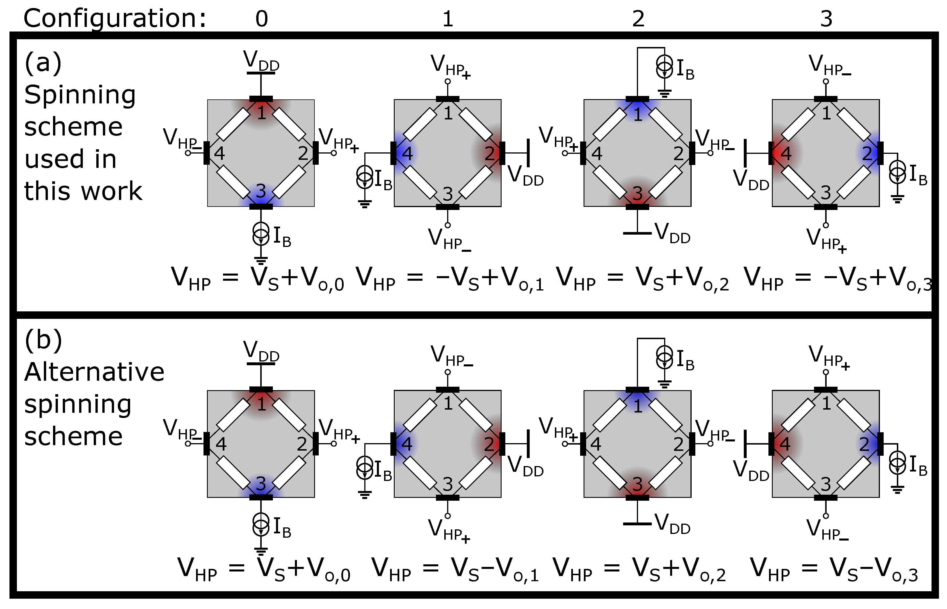
2.1. Hall Plate Readout Configuration and Static Offsets
2.2. Classical Four-Phase Hall Plate Spinning
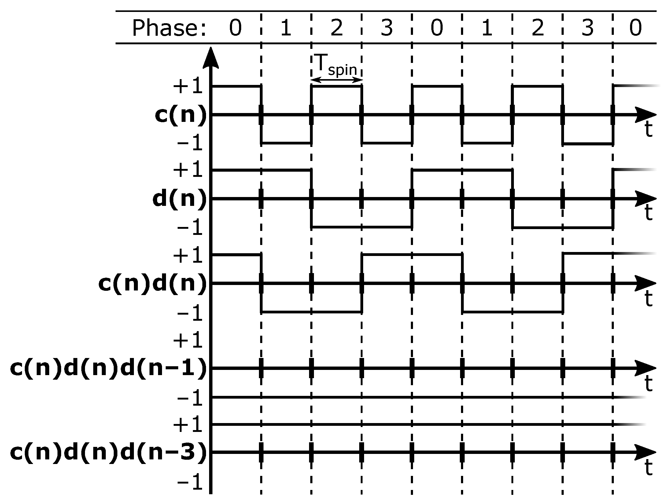
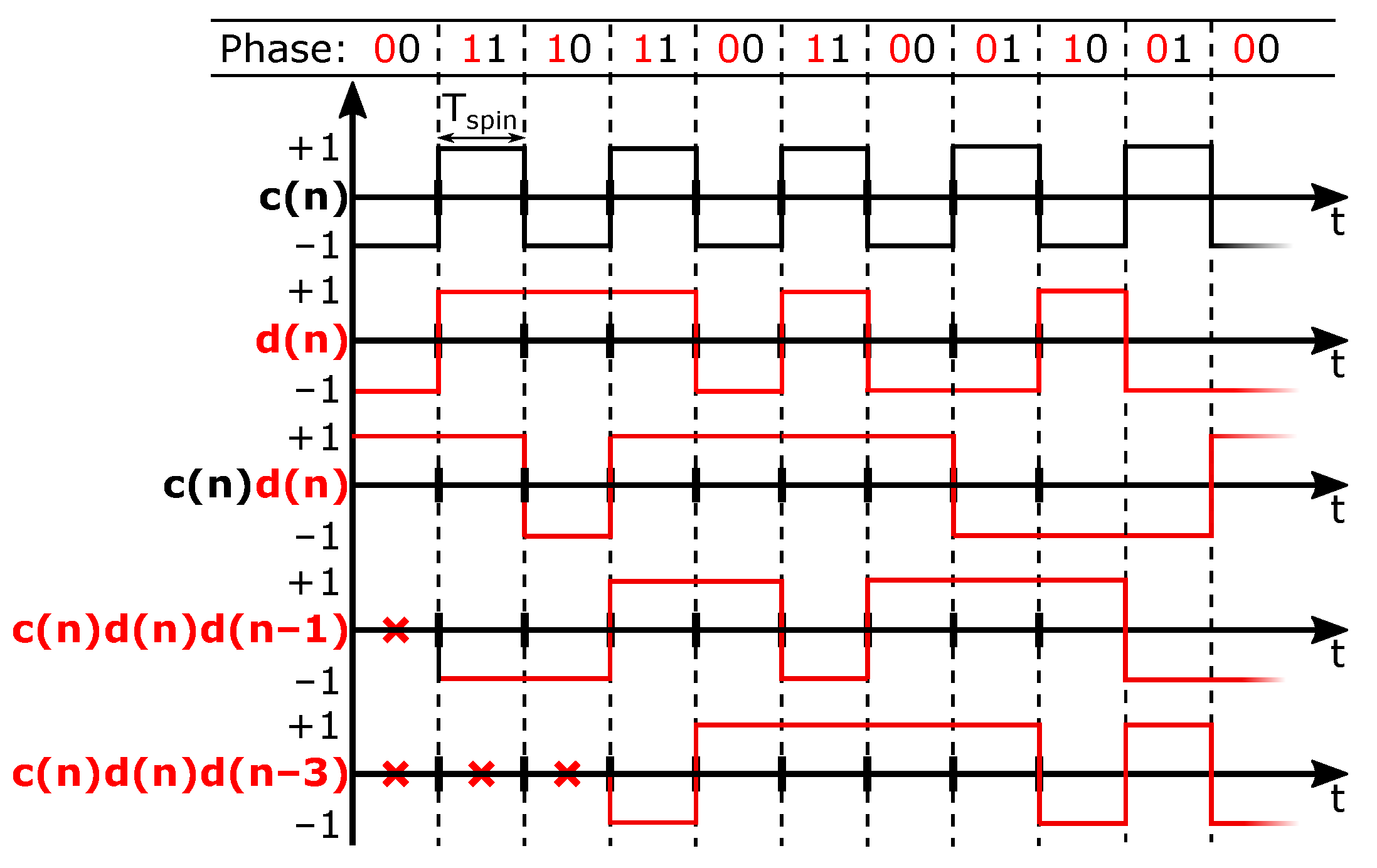
2.3. Randomized Four-Phase Hall Plate Spinning
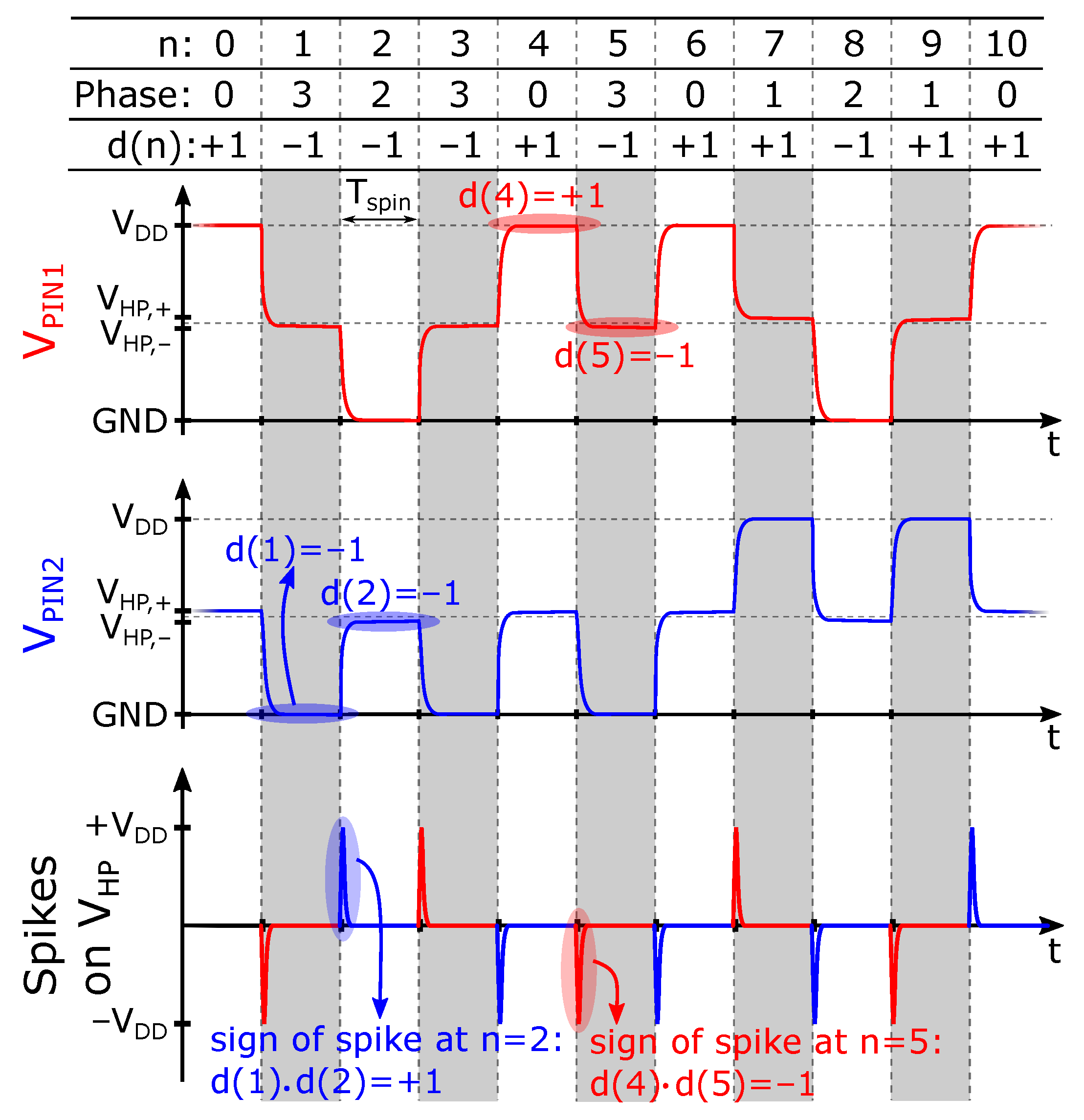
2.4. Dynamic Spinning Effects
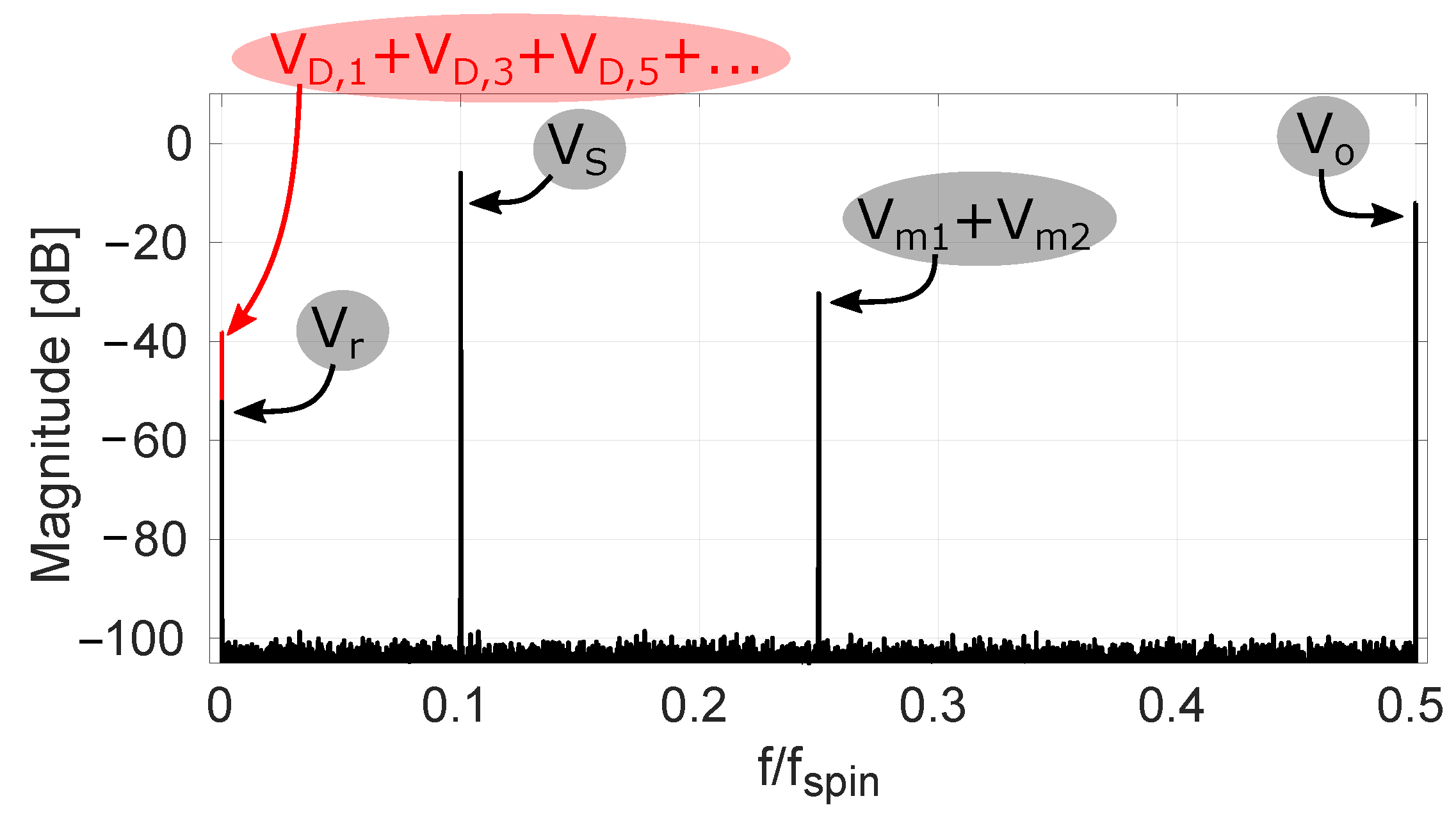
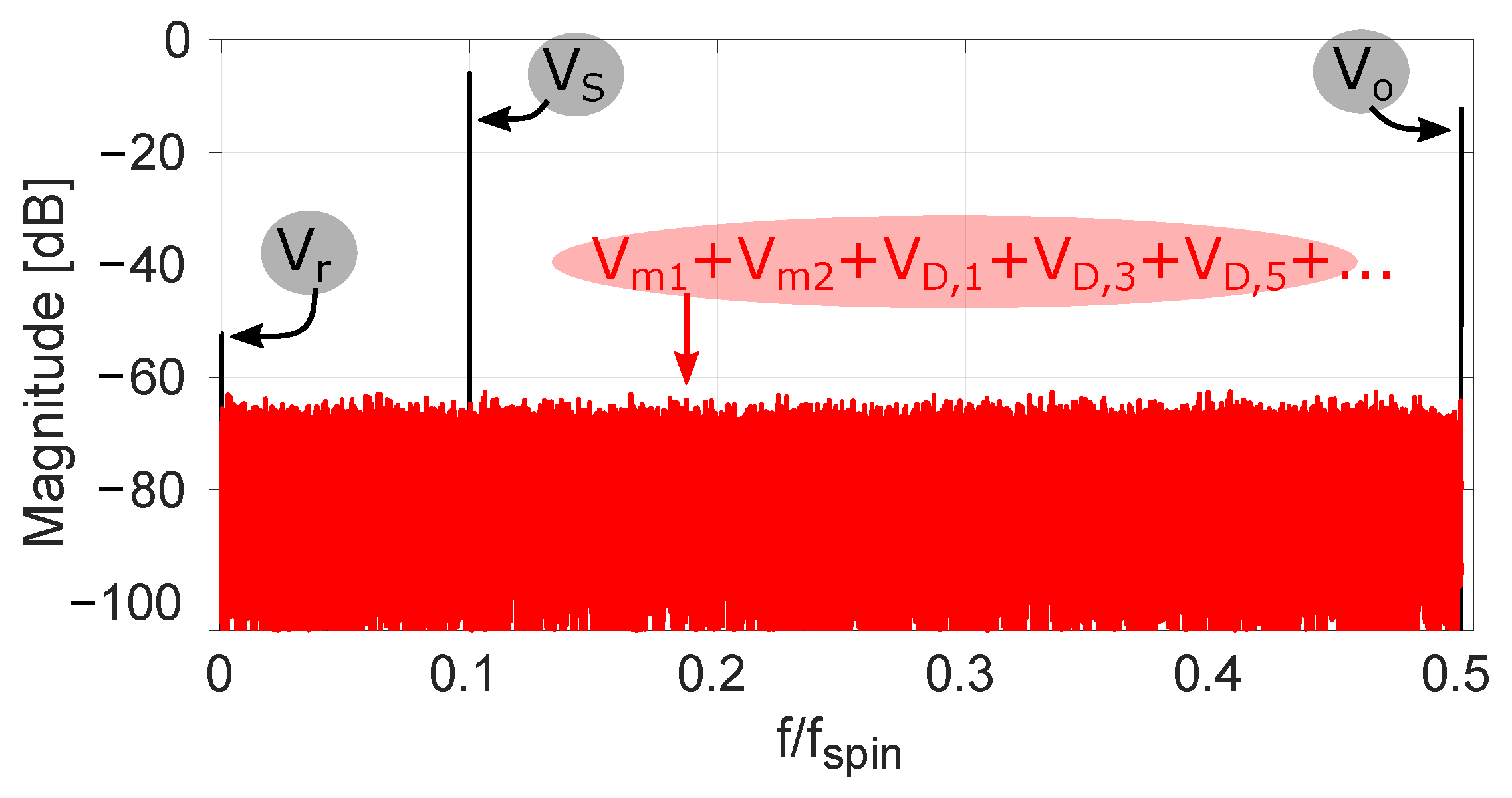
2.5. Modulations Obtained with Randomized Spinning
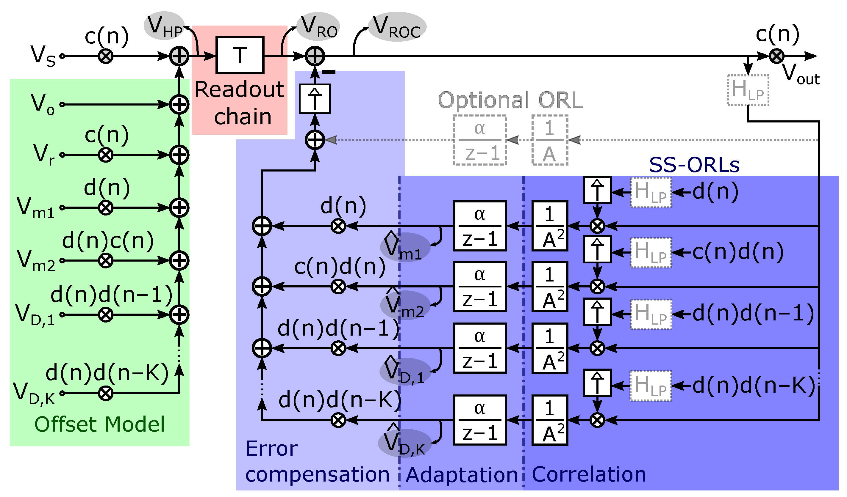
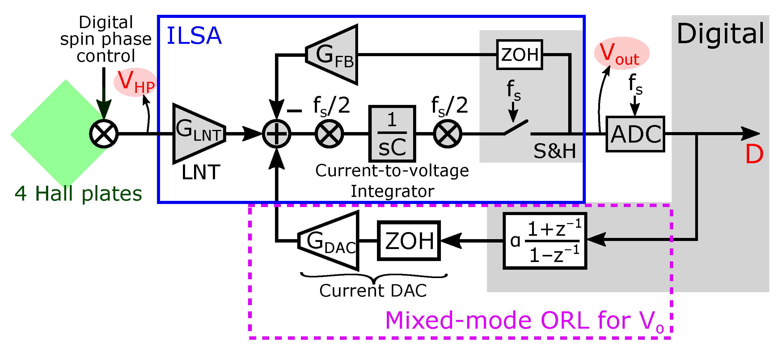
2.6. System-Level Overview of the Proposed Offset-Suppression Solution
3. Spread-Spectrum Offset Reduction Loops
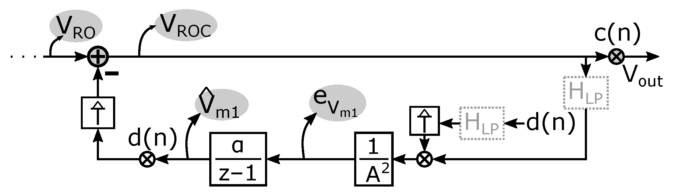
3.1. System Derivation
3.2. Sizing the SS-ORL’s Integration Factor
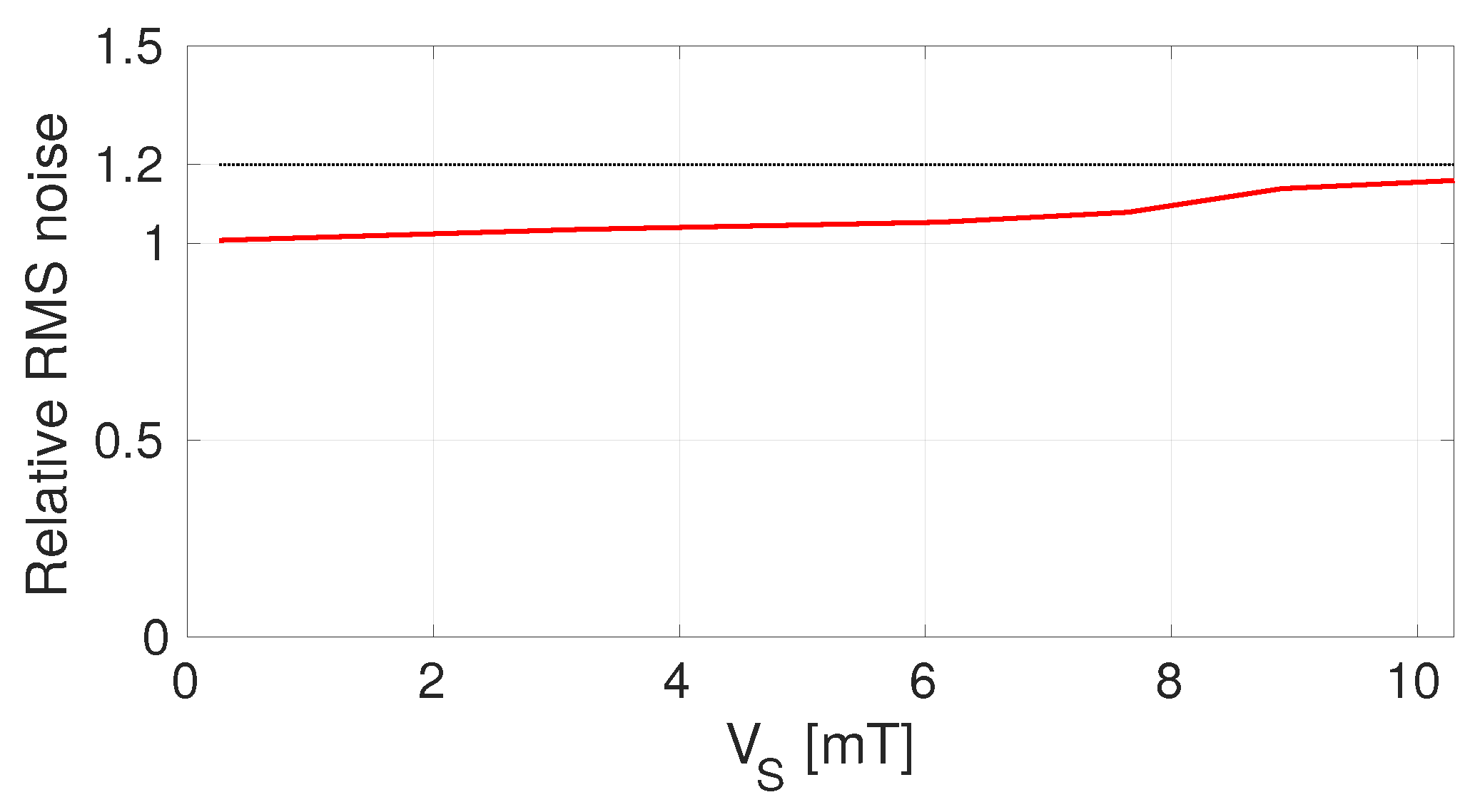
3.2.1. Noise of the SS-ORLs
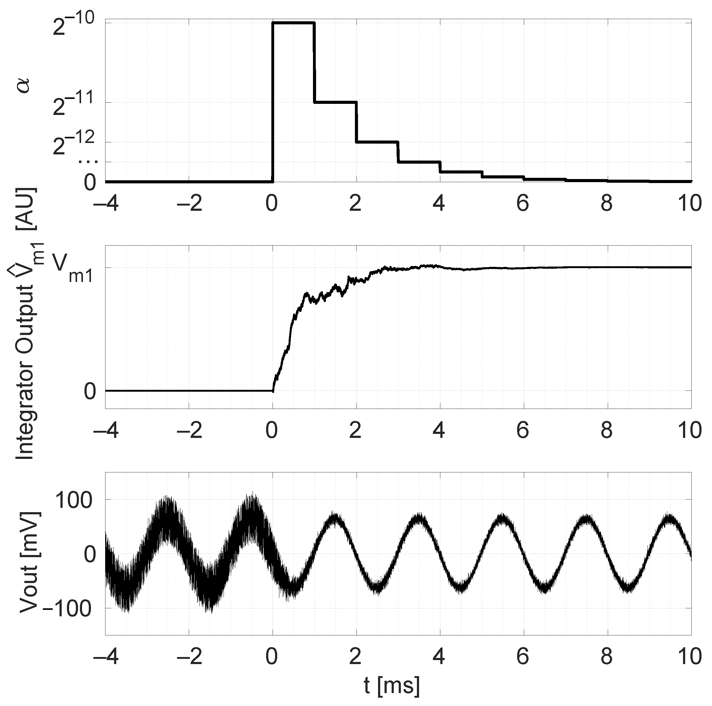
3.2.2. Start-Up Time of the SS-ORLs
3.2.3. Discussion
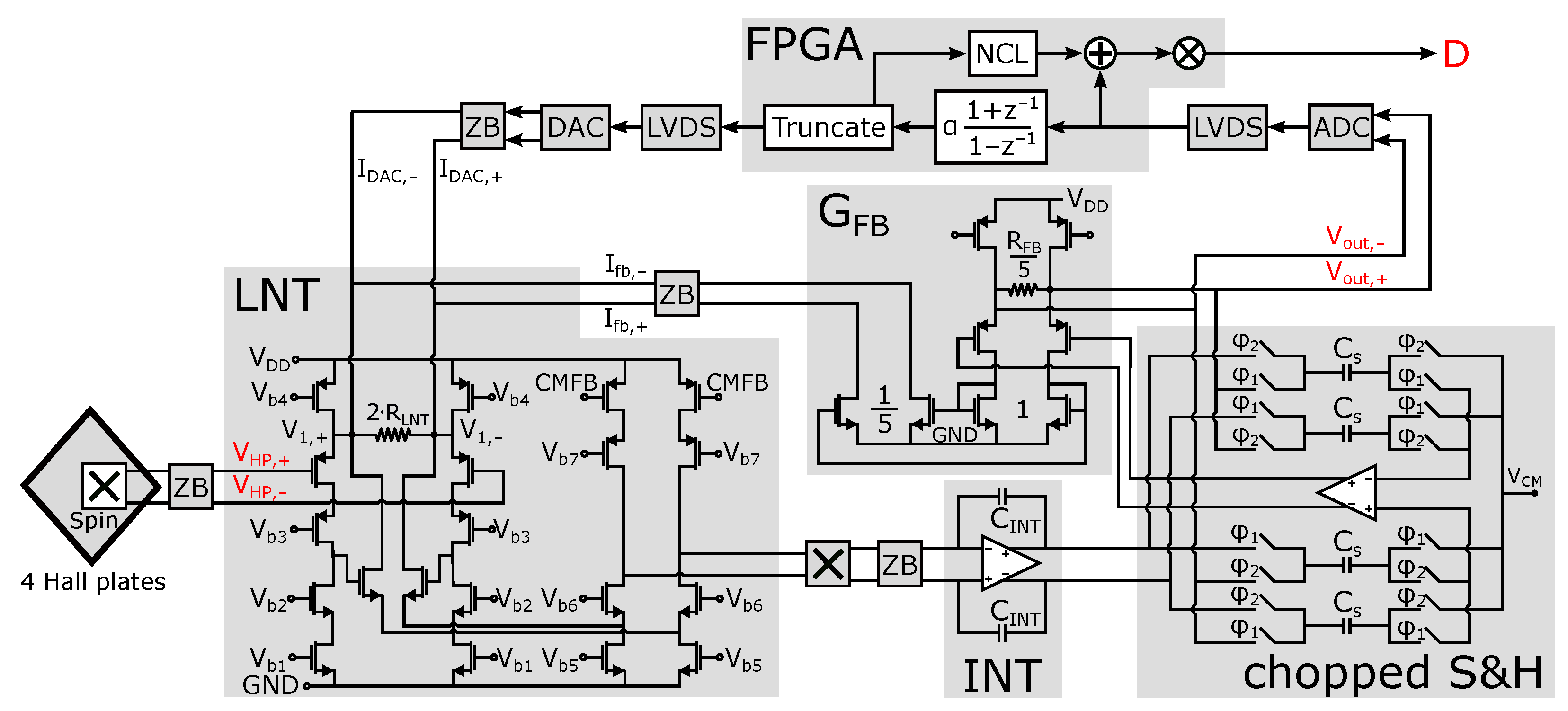
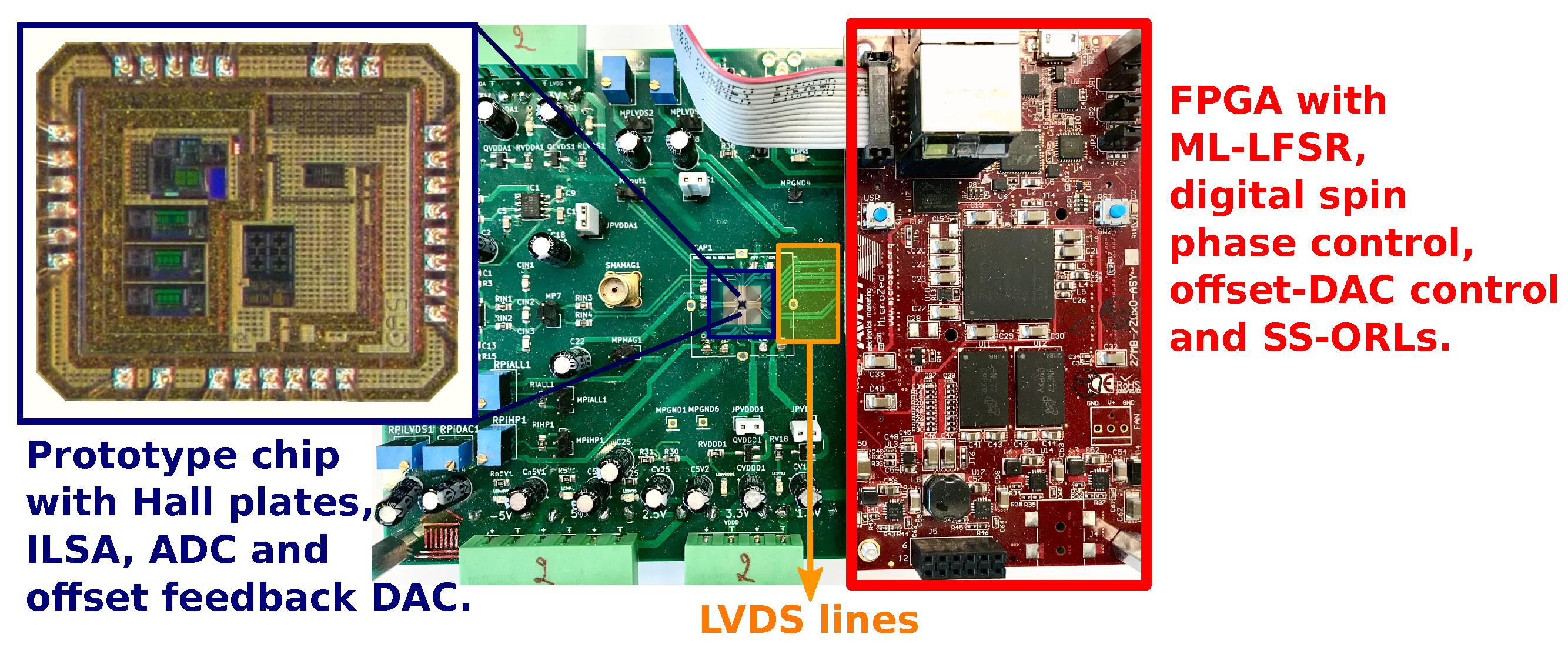
4. The 2 MS/s Hall System Prototype
5. Experimental Verification
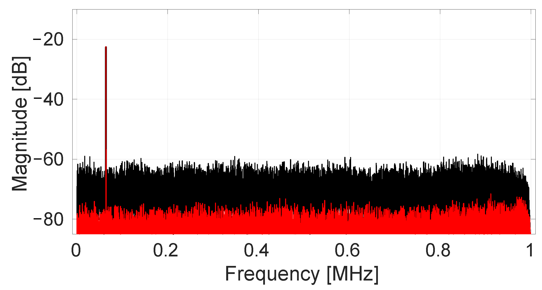
5.1. Measurements with Noise-Constrained Value
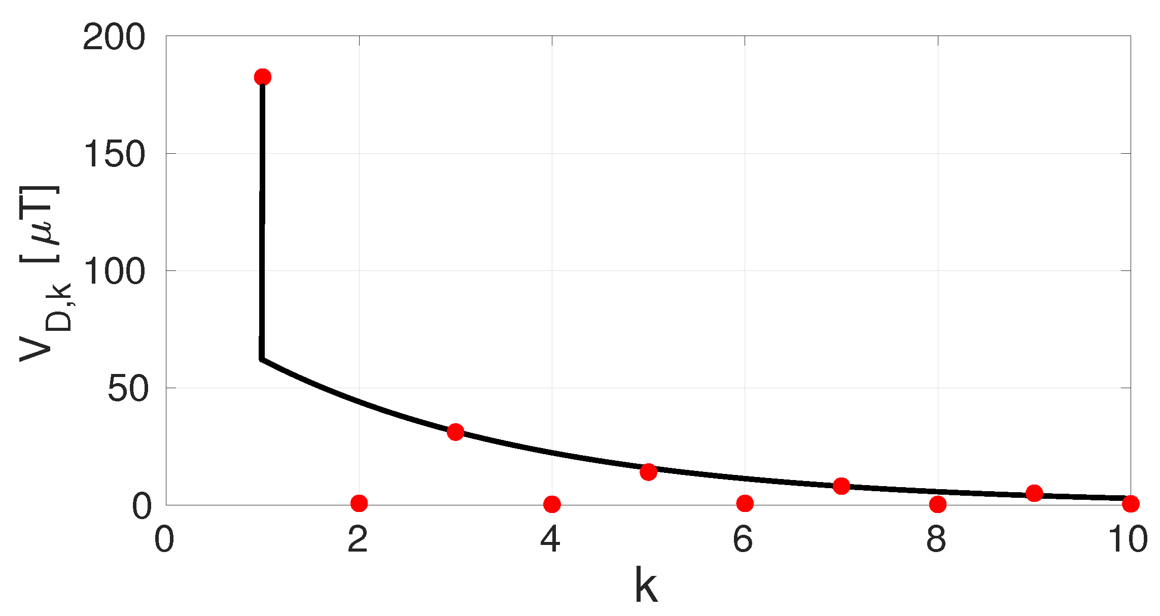
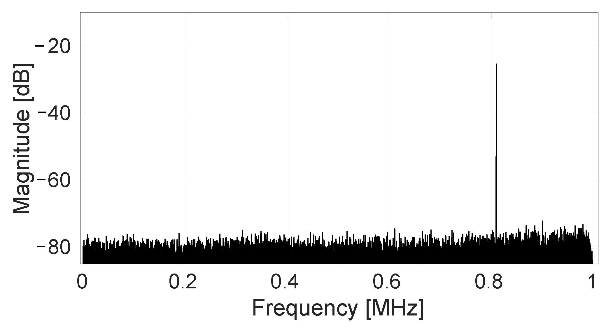
5.2. Measurements with Stepped Values
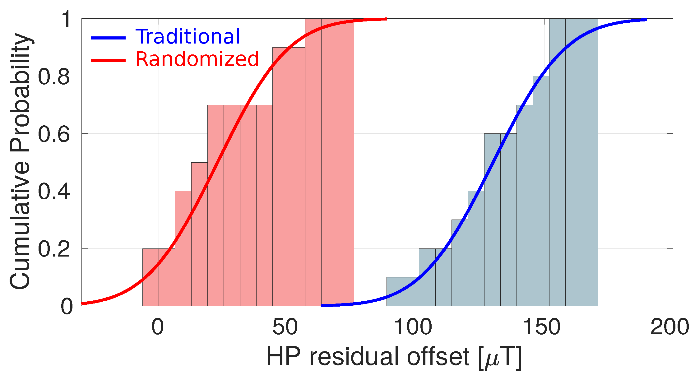
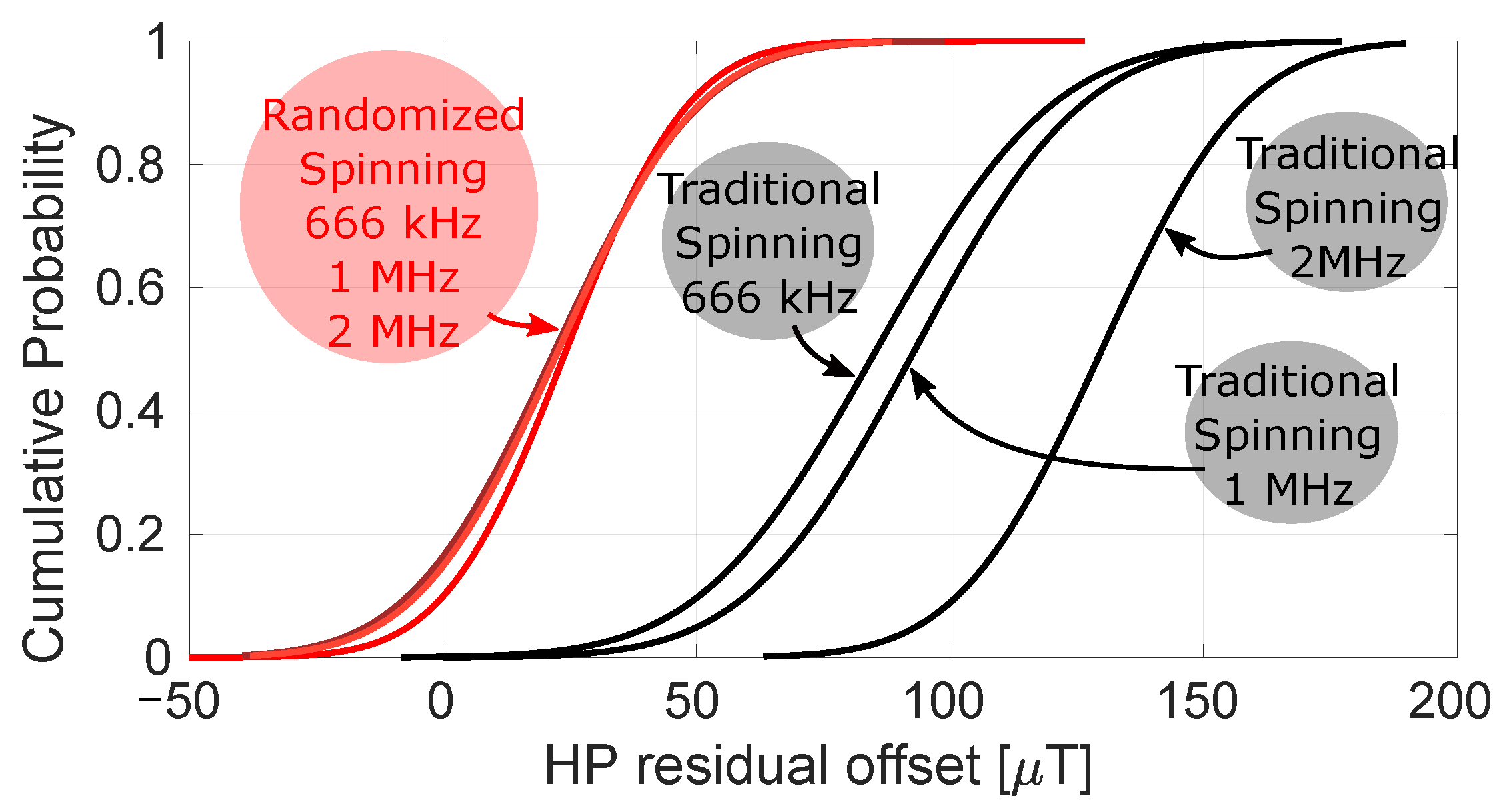
5.3. Offset Histograms
6. Conclusions
Author Contributions
Funding
Institutional Review Board Statement
Informed Consent Statement
Data Availability Statement
Conflicts of Interest
References
- Jiang, J.; Makinwa, K.A.A. Multipath Wide-Bandwidth CMOS Magnetic Sensors. IEEE J. Solid-State Circuits 2017, 52, 198–209. [Google Scholar] [CrossRef]
- Jiang, J.; Makinwa, K.A.A. A Hybrid Multi-Path CMOS Magnetic Sensor with 76 ppm/°C Sensitivity Drift and Discrete-Time Ripple Reduction Loops. IEEE J. Solid-State Circuits 2017, 52, 1876–1884. [Google Scholar] [CrossRef]
- Ziegler, S.; Woodward, R.C.; Iu, H.H.C.; Borle, L.J. Current Sensing Techniques: A Review. IEEE Sens. J. 2009, 9, 354–376. [Google Scholar] [CrossRef]
- Ripka, P. Electric current sensors: A review. Meas. Sci. Technol. 2010, 21, 112001. [Google Scholar] [CrossRef]
- Patel, A.; Ferdowsi, M. Current Sensing for Automotive Electronics—A Survey. IEEE Trans. Veh. Technol. 2009, 58, 4108–4119. [Google Scholar] [CrossRef]
- Burger, F.; Besse, P.A.; Popovic, R. New fully integrated 3-D silicon Hall sensor for precise angular-position measurements. Sens. Actuators A Phys. 1998, 67, 72–76. [Google Scholar] [CrossRef]
- Fan, H.; Li, S.; Nabaei, V.; Feng, Q.; Heidari, H. Modeling of Three-Axis Hall Effect Sensors Based on Integrated Magnetic Concentrator. IEEE Sens. J. 2020, 20, 9919–9927. [Google Scholar] [CrossRef]
- Baltes, H.; Popovic, R. Integrated semiconductor magnetic field sensors. Proc. IEEE 1986, 74, 1107–1132. [Google Scholar] [CrossRef]
- Munter, P. A Low-offset Spinning-current Hall Plate. Sens. Actuators A Phys. 1990, 22, 743–746. [Google Scholar] [CrossRef]
- Popovic, R.S. Hall Effect Devices; Institute of Physics Publishing: Bristol, UK, 2004. [Google Scholar]
- Enz, C.C.; Temes, G.C. Circuit techniques for reducing the effects of op-amp imperfections: Autozeroing, correlated double sampling, and chopper stabilization. Proc. IEEE 1996, 84, 1584–1614. [Google Scholar] [CrossRef]
- Jiang, J.; Kindt, W.J.; Makinwa, K.A.A. A Continuous-Time Ripple Reduction Technique for Spinning-Current Hall Sensors. IEEE J. Solid-State Circuits 2014, 7, 1525–1534. [Google Scholar] [CrossRef]
- Riem, R.; Raman, J.; Borgmans, J.; Rombouts, P. A Low-Noise Instrumentation Amplifier with Built-in Anti-Aliasing for Hall Sensors. IEEE Sens. J. 2021, 21, 18932–18944. [Google Scholar] [CrossRef]
- Wu, R.; Makinwa, K.A.A.; Huijsing, J.H. A Chopper Current-Feedback Instrumentation Amplifier with a 1 mHz 1/f Noise Corner and an AC-Coupled Ripple Reduction Loop. IEEE J. Solid-State Circuits 2009, 44, 3232–3243. [Google Scholar] [CrossRef]
- Motz, M.; Ausserlechner, U.; Bresch, M.; Fakesch, U.; Schaffer, B.; Reidl, C.; Scherr, W.; Pircher, G.; Strasser, M.; Strutz, V. A miniature digital current sensor with differential Hall probes using enhanced chopping techniques and mechanical stress compensation. In Proceedings of the SENSORS, 2012 IEEE, Taipei, Taiwan, 28–31 October 2012; pp. 1–4. [Google Scholar] [CrossRef]
- Jiang, H.; Nihtianov, S.; Makinwa, K.A.A. An Energy-Efficient 3.7-nV/√Hz Bridge Readout IC with a Stable Bridge Offset Compensation Scheme. IEEE J. Solid-State Circuits 2019, 54, 856–864. [Google Scholar] [CrossRef]
- Wei, R.; Liu, Z.; Zhu, R. Low noise chopper-stabilized instrumentation amplifier with a ripple reduction loop. Analog Integr. Circuits Signal Process. 2018, 96, 521–529. [Google Scholar] [CrossRef]
- Pastre, M.; Kayal, M.; Blanchard, H. A Hall Sensor Analog Front End for Current Measurement with Continuous Gain Calibration. IEEE Sens. J. 2007, 7, 860–867. [Google Scholar] [CrossRef]
- Leroy, S.; Rigert, S.; Laville, A.; Ajbl, A.; Close, G.F. Integrated hall-based magnetic platform for position sensing. In Proceedings of the ESSCIRC 2017-43rd IEEE European Solid State Circuits Conference, Leuven, Belgium, 11–14 September 2017; pp. 360–363. [Google Scholar] [CrossRef]
- Crescentini, M.; Syeda, S.F.; Gibiino, G.P. Hall-Effect Current Sensors: Principles of Operation and Implementation Techniques. IEEE Sens. J. 2022, 22, 10137–10151. [Google Scholar] [CrossRef]
- Huber, S.; Leten, W.; Ackermann, M.; Schott, C.; Paul, O. A Fully Integrated Analog Compensation for the Piezo-Hall Effect in a CMOS Single-Chip Hall Sensor Microsystem. IEEE Sens. J. 2015, 15, 2924–2933. [Google Scholar] [CrossRef]
- Raman, J.; Rombouts, P. Randomized Spinning of Hall Plates. U.S. Patent 10,739,418, 5 July 2019. [Google Scholar]
- Crescentini, M.; Marchesi, M.; Romani, A.; Tartagni, M.; Traverso, P.A. A Broadband, On-Chip Sensor Based on Hall Effect for Current Measurements in Smart Power Circuits. IEEE Trans. Instrum. Meas. 2018, 67, 1470–1485. [Google Scholar] [CrossRef]
- Kaufmann, T.; Kopp, D.; Purkl, F.; Baumann, M.; Ruther, P.; Paul, O. Piezoresistive Response of Vertical Hall Devices. IEEE Sensors J. 2011, 11, 2628–2635. [Google Scholar] [CrossRef]
- Taranow, S.G. Method for the compensation of the nonequipotential voltage in the Hall voltage and means for its realization. German Patent Application 2333080, 9 December 1973. [Google Scholar]
- Bilotti, A.; Monreal, G.; Vig, R. Monolithic Magnetic Hall Sensor Using Dynamic Quadrature Offset Cancellation. IEEE J. Solid-State Circuits 1997, 32, 829–839. [Google Scholar] [CrossRef]
- Ajbl, A.; Pastre, M.; Kayal, M. A Fully Integrated Hall Sensor Microsystem for Contactless Current Measurement. IEEE Sensors J. 2013, 13, 2271–2278. [Google Scholar] [CrossRef]
- Randjelovic, Z.; Kayal, M.; Popovic, R.; Blanchard, H. Highly sensitive Hall magnetic sensor microsystem in CMOS technology. IEEE J. Solid-State Circuits 2002, 37, 151–159. [Google Scholar] [CrossRef]
- Udo, A. Limits of offset cancellation by the principle of spinning current Hall probe. In Proceedings of the SENSORS, 2004 IEEE, Vienna, Austria, 24–27 October 2004; Volume 3, pp. 1117–1120. [Google Scholar] [CrossRef]
- Steiner, R.; Maier, C.; Hàberli, A.; Steiner, F.P.; Baltes, H. Offset reduction in Hall devices by continuous spinning current method. Sensors Actuators A Phys. 1998, 66, 167–172. [Google Scholar] [CrossRef]
- Tang, A. Bandpass spread spectrum clocking for reduced clock spurs in autozeroed amplifiers. In Proceedings of the ISCAS 2001. The 2001 IEEE International Symposium on Circuits and Systems (Cat. No. 01CH37196), Sydney, Australia, 6–9 May 2001; Volume 1, pp. 663–666. [Google Scholar] [CrossRef]
- Ivanov, V.; Shaik, M. 5.1 A 10 MHz-bandwidth 4 μs-large-signal-settling 6.5 nV/√Hz-noise 2 μV-offset chopper operational amplifier. In Proceedings of the 2016 IEEE International Solid-State Circuits Conference (ISSCC), San Francisco, CA, USA, 31 January–4 February 2016; pp. 88–89. [Google Scholar] [CrossRef]
- Petkov, V.P.; Balachandran, G.K.; Beintner, J. A Fully Differential Charge-Balanced Accelerometer for Electronic Stability Control. IEEE J. Solid-State Circuits 2014, 49, 262–270. [Google Scholar] [CrossRef]
- Lanniel, A.; Boeser, T.; Alpert, T.; Ortmanns, M. Tackling SDM Feedback Coefficient Modulation in Area Optimized Frontend Readout Circuit for High Performance MEMS Accelerometers. In Proceedings of the 2019 IEEE International Symposium on Inertial Sensors and Systems (INERTIAL), Naples, FL, USA, 1–5 April 2019; pp. 1–4. [Google Scholar] [CrossRef]
- Lanniel, A.; Boeser, T.; Alpert, T.; Ortmanns, M. Low-Noise Readout Circuit for an Automotive MEMS Accelerometer. IEEE Open J. Solid-State Circuits Soc. 2021, 1, 140–148. [Google Scholar] [CrossRef]
- Wang, C.B. A 20-bit 25-kHz Delta–Sigma A/D Converter Utilizing a Frequency-Shaped Chopper Stabilization Scheme. IEEE J. Solid-State Circuits 2001, 36, 566–569. [Google Scholar] [CrossRef]
- Bakker, A.; Thiele, K.; Huijsing, J. A CMOS nested-chopper instrumentation amplifier with 100-nV offset. IEEE J. Solid-State Circuits 2000, 35, 1877–1883. [Google Scholar] [CrossRef]
- Keane, J.; Hurst, P.; Lewis, S. Background interstage gain calibration technique for pipelined ADCs. IEEE Trans. Circuits Syst. I Regul. Pap. 2005, 52, 32–43. [Google Scholar] [CrossRef]
- Panigada, A.; Galton, I. A 130 mW 100 MS/s Pipelined ADC with 69 dB SNDR Enabled by Digital Harmonic Distortion Correction. IEEE J. Solid-State Circuits 2009, 44, 3314–3328. [Google Scholar] [CrossRef]
- Taylor, G.; Galton, I. A Mostly-Digital Variable-Rate Continuous-Time Delta-Sigma Modulator ADC. IEEE J. Solid-State Circuits 2010, 45, 2634–2646. [Google Scholar] [CrossRef]
- Kauffman, J.G.; Witte, P.; Becker, J.; Ortmanns, M. An 8.5 mW Continuous-Time ΔΣ Modulator with 25 MHz Bandwidth Using Digital Background DAC Linearization to Achieve 63.5 dB SNDR and 81 dB SFDR. IEEE J. Solid-State Circuits 2011, 46, 2869–2881. [Google Scholar] [CrossRef]
- Huang, J.; Mercier, P.P. A 112-dB SFDR 89-dB SNDR VCO-Based Sensor Front-End Enabled by Background-Calibrated Differential Pulse Code Modulation. IEEE J. Solid-State Circuits 2021, 56, 1046–1057. [Google Scholar] [CrossRef]
- Robbins, H.; Monro, S. A Stochastic Approximation Method. Ann. Math. Stat. 1951, 22, 400–407. [Google Scholar] [CrossRef]
- Gray, P.R.; Hurst, P.J.; Lewis, S.H.; Meyer, R.G. Analysis and Design of Analog Integrated Circuits; John Wiley & Sons Inc.: New York, NY, USA, 2009; pp. 212–213. [Google Scholar]
- Heidari, H.; Bonizzoni, E.; Gatti, U.; Maloberti, F. A CMOS Current-Mode Magnetic Hall Sensor with Integrated Front-End. IEEE Trans. Circuits Syst.-I Regul. Pap. 2015, 62, 1270–1278. [Google Scholar] [CrossRef]


| 23 | 37 | 122 | 116 | 183 | 31 | 14 | 8 | |
| 22 | 3455 | 40 | 51 | 11 | 2 | 1.3 | 0.8 |
| This Work | [13] | [2] | [23] | [45] | |
|---|---|---|---|---|---|
| Hall | Hall | Hall | Hall | Hall | |
| Inp. range [mT] | ±10.6 | ±10.6 | ±12.5 | ±14.8 | 10 |
| Noise [] | 52–63 * | 55 | 430 | 136 | - |
| Typ. offset [T] | 74 ** 23 | 68 | 40 | >14,000 | <50 |
| BW [kHz] | 820 *** | 410 | 400 | 1000 | 7.8 |
| Current [mA] | 5.1 † | 5.1 | 8 | 8.8 | 0.067 |
| [s] | 0.5 | 1 | 25 | 0.0625 | 1 |
Publisher’s Note: MDPI stays neutral with regard to jurisdictional claims in published maps and institutional affiliations. |
© 2022 by the authors. Licensee MDPI, Basel, Switzerland. This article is an open access article distributed under the terms and conditions of the Creative Commons Attribution (CC BY) license (https://creativecommons.org/licenses/by/4.0/).
Share and Cite
Riem, R.; Raman, J.; Rombouts, P. A 2 MS/s Full Bandwidth Hall System with Low Offset Enabled by Randomized Spinning. Sensors 2022, 22, 6069. https://doi.org/10.3390/s22166069
Riem R, Raman J, Rombouts P. A 2 MS/s Full Bandwidth Hall System with Low Offset Enabled by Randomized Spinning. Sensors. 2022; 22(16):6069. https://doi.org/10.3390/s22166069
Chicago/Turabian StyleRiem, Robbe, Johan Raman, and Pieter Rombouts. 2022. "A 2 MS/s Full Bandwidth Hall System with Low Offset Enabled by Randomized Spinning" Sensors 22, no. 16: 6069. https://doi.org/10.3390/s22166069
APA StyleRiem, R., Raman, J., & Rombouts, P. (2022). A 2 MS/s Full Bandwidth Hall System with Low Offset Enabled by Randomized Spinning. Sensors, 22(16), 6069. https://doi.org/10.3390/s22166069