

Robust Achromatic All-Dielectric Metalens for Infrared Detection in Intelligent Inspection


Abstract
:1. Introduction
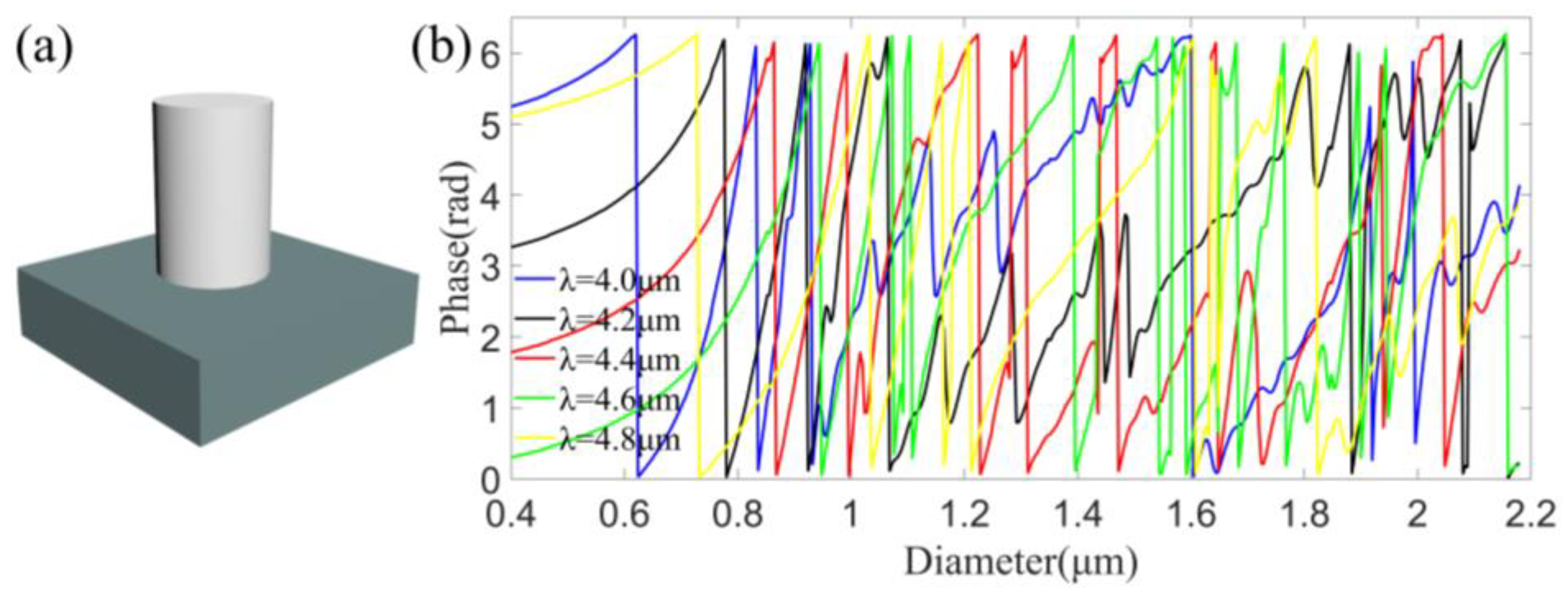
2. Methods
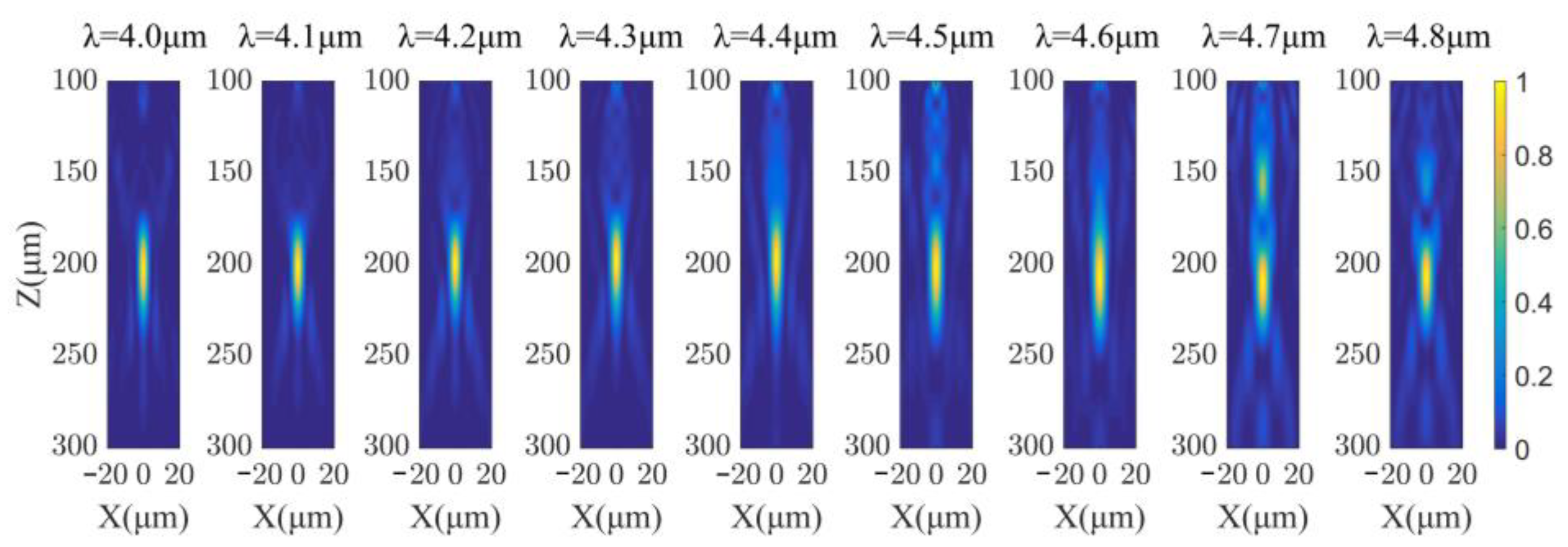
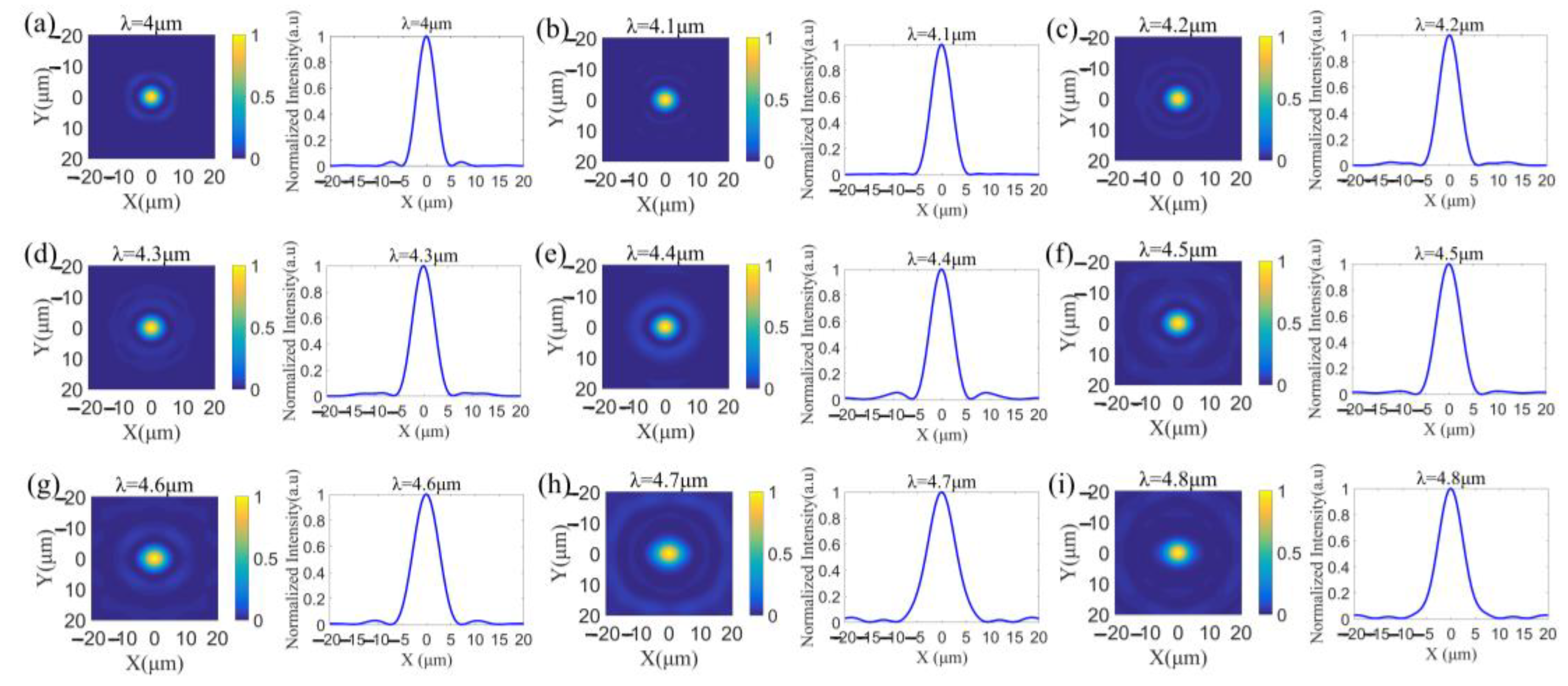
3. Results
4. Conclusions
Supplementary Materials
Author Contributions
Funding
Institutional Review Board Statement
Informed Consent Statement
Data Availability Statement
Acknowledgments
Conflicts of Interest
References
- Khorasaninejad, M.; Capasso, F. Metalenses: Versatile multifunctional photonic components. Science 2017, 358, eaam8100. [Google Scholar] [CrossRef] [PubMed]
- Verslegers, L.; Catrysse, P.B.; Yu, Z.F.; White, J.S.; Barnard, E.S.; Brongersma, M.L.; Fan, S.H. Planar Lenses Based on Nanoscale Slit Arrays in a Metallic Film. Nano Lett. 2009, 9, 235–238. [Google Scholar] [CrossRef]
- Yu, N.F.; Genevet, P.; Kats, M.A.; Aieta, F.; Tetienne, J.P.; Capasso, F.; Gaburro, Z. Light Propagation with Phase Discontinuities: Generalized Laws of Reflection and Refraction. Science 2011, 334, 333–337. [Google Scholar] [CrossRef]
- Aieta, F.; Genevet, P.; Kats, M.A.; Yu, N.F.; Blanchard, R.; Gahurro, Z.; Capasso, F. Aberration-Free Ultrathin Flat Lenses and Axicons at Telecom Wavelengths Based on Plasmonic Metasurfaces. Nano Lett. 2012, 12, 4932–4936. [Google Scholar] [CrossRef] [PubMed]
- Ni, X.J.; Emani, N.K.; Kildishev, A.V.; Boltasseva, A.; Shalaev, V.M. Broadband Light Bending with Plasmonic Nanoantennas. Science 2012, 335, 427. [Google Scholar] [CrossRef]
- Ni, X.J.; Ishii, S.; Kildishev, A.V.; Shalaev, V.M. Ultra-thin, planar, Babinet-inverted plasmonic metalenses. Light-Sci. Appl. 2013, 2, e72. [Google Scholar] [CrossRef]
- Pors, A.; Nielsen, M.G.; Eriksen, R.L.; Bozhevolnyi, S.I. Broadband Focusing Flat Mirrors Based on Plasmonic Gradient Metasurfaces. Nano Lett. 2013, 13, 829–834. [Google Scholar] [CrossRef] [PubMed]
- Aieta, F.; Kats, M.A.; Genevet, P.; Capasso, F. Multiwavelength achromatic metasurfaces by dispersive phase compensation. Science 2015, 347, 1342–1345. [Google Scholar] [CrossRef]
- Arbabi, A.; Horie, Y.; Ball, A.J.; Bagheri, M.; Faraon, A. Subwavelength-thick lenses with high numerical apertures and large efficiency based on high-contrast transmitarrays. Nat. Commun. 2015, 6, 7069. [Google Scholar] [CrossRef]
- Wang, W.; Guo, Z.Y.; Li, R.Z.; Zhang, J.R.; Liu, Y.; Wang, X.S.; Qu, S.L. Ultra-thin, planar, broadband, dual-polarity plasmonic metalens. Photonics Res. 2015, 3, 68–71. [Google Scholar] [CrossRef] [Green Version]
- Arbabi, A.; Arbabi, E.; Kamali, S.M.; Horie, Y.; Han, S.; Faraon, A. Miniature optical planar camera based on a wide-angle metasurface doublet corrected for monochromatic aberrations. Nat. Commun. 2016, 7, 13682. [Google Scholar] [CrossRef]
- Khorasaninejad, M.; Chen, W.T.; Devlin, R.C.; Oh, J.; Zhu, A.Y.; Capasso, F. Metalenses at visible wavelengths: Diffraction-limited focusing and subwavelength resolution imaging. Science 2016, 352, 1190–1194. [Google Scholar] [CrossRef]
- Khorasaninejad, M.; Chen, W.T.; Zhu, A.Y.; Oh, J.; Devlin, R.C.; Rousso, D.; Capasso, F. Multispectral Chiral Imaging with a Metalens. Nano Lett. 2016, 16, 4595–4600. [Google Scholar] [CrossRef]
- Khorasaninejad, M.; Zhuit, A.Y.; Roques-Carmes, C.; Chen, W.T.; Oh, J.; Mishra, I.; Devlin, R.C.; Capasso, F. Polarization-Insensitive Metalenses at Visible Wavelengths. Nano Lett. 2016, 16, 7229–7234. [Google Scholar] [CrossRef]
- Groever, B.; Chen, W.T.; Capasso, F. Meta-Lens Doublet in the Visible Region. Nano Lett. 2017, 17, 4902–4907. [Google Scholar] [CrossRef]
- Khorasaninejad, M.; Shi, Z.; Zhu, A.Y.; Chen, W.T.; Sanjeev, V.; Zaidi, A.; Capasso, F. Achromatic Metalens over 60 nm Bandwidth in the Visible and Metalens with Reverse Chromatic Dispersion. Nano Lett. 2017, 17, 1819–1824. [Google Scholar] [CrossRef]
- Li, K.; Guo, Y.H.; Pu, M.B.; Li, X.; Ma, X.L.; Zhao, Z.Y.; Luo, X.G. Dispersion controlling meta-lens at visible frequency. Opt. Express 2017, 25, 21419–21427. [Google Scholar] [CrossRef]
- Chen, W.T.; Zhu, A.Y.; Sanjeev, V.; Khorasaninejad, M.; Shi, Z.J.; Lee, E.; Capasso, F. A broadband achromatic metalens for focusing and imaging in the visible. Nat. Nanotechnol. 2018, 13, 220–226. [Google Scholar] [CrossRef]
- Shrestha, S.; Overvig Adam, C.; Lu, M.; Stein, A.; Yu, N. Broadband achromatic dielectric metalenses. Light Sci. Appl. 2018, 7, 85. [Google Scholar] [CrossRef]
- Wang, S.; Wu, P.C.; Su, V.C.; Lai, Y.C.; Chen, M.K.; Kuo, H.Y.; Chen, B.H.; Chen, Y.H.; Huang, T.T.; Wang, J.H.; et al. A broadband achromatic metalens in the visible. Nat. Nanotechnol. 2018, 13, 227–232. [Google Scholar] [CrossRef]
- Shi, Z.; Khorasaninejad, M.; Huang, Y.W.; Roques-Carmes, C.; Zhu, A.Y.; Chen, W.T.; Sanjeev, V.; Ding, Z.W.; Tamagnone, M.; Chaudhary, K.; et al. Single-Layer Metasurface with Controllable Multiwavelength Functions. Nano Lett. 2018, 18, 2420–2427. [Google Scholar] [CrossRef]
- Hsiao, H.H.; Chen, Y.H.; Lin, R.J.; Wu, P.C.; Wang, S.; Chen, B.H.; Tsai, D.P. Integrated Resonant Unit of Metasurfaces for Broadband Efficiency and Phase Manipulation. Adv. Opt. Mater. 2018, 6, 1800031. [Google Scholar] [CrossRef]
- Zhou, Y.; Kravchenko, I.I.; Wang, H.; Nolen, J.R.; Gu, G.; Valentine, J. Multilayer Noninteracting Dielectric Metasurfaces for Multiwavelength Metaoptics. Nano Lett. 2018, 18, 7529–7537. [Google Scholar] [CrossRef] [PubMed]
- Lin, R.J.; Su, V.C.; Wang, S.M.; Chen, M.K.; Chung, T.L.; Chen, Y.H.; Kuo, H.Y.; Chen, J.W.; Chen, J.; Huang, Y.T.; et al. Achromatic metalens array for full-colour light-field imaging. Nat. Nanotechnol. 2019, 14, 227–231. [Google Scholar] [CrossRef] [PubMed]
- Chen, W.T.; Zhu, A.Y.; Sisler, J.; Bharwani, Z.; Capasso, F. A broadband achromatic polarization-insensitive metalens consisting of anisotropic nanostructures. Nat. Commun. 2019, 10, 355. [Google Scholar] [CrossRef] [PubMed]
- Chen, L.; Hao, Y.; Zhao, L.; Wu, R.H.; Liu, Y.; Wei, Z.C.; Xu, N.; Li, Z.T.; Liu, H.Z. Multifunctional metalens generation using bilayer all-dielectric metasurfaces. Opt. Express 2021, 29, 18304. [Google Scholar] [CrossRef] [PubMed]
- Elsawy, M.M.R.; Gourdin, A.; Binois, M.; Duvigneau, R.; Felbacq, D.; Khadir, S.; Genevet, P.; Lanteri, S. Multiobjective Statistical Learning Optimization of RGB Metalens. ACS Photonics 2021, 8, 2498–2508. [Google Scholar] [CrossRef]
- Lim, S.W.D.; Meretska, M.L.; Capasso, F. A High Aspect Ratio Inverse-Designed Holey Metalens. Nano Lett. 2021, 21, 8642–8649. [Google Scholar] [CrossRef]
- Mohtashami, Y.; DeCrescent, R.A.; Heki, L.K.; Iyer, P.P.; Butakov, N.A.; Wong, M.S.; Alhassan, A.; Mitchell, W.J.; Nakamura, S.; DenBaars, S.P.; et al. Light-emitting metalenses and meta-axicons for focusing and beaming of spontaneous emission. Nat. Commun. 2021, 12, 3591. [Google Scholar] [CrossRef]
- Lu, X.J.; Guo, Y.H.; Pu, M.B.; Zhang, Y.X.; Li, Z.; Li, X.; Ma, X.L.; Luo, X.G. Broadband achromatic metasurfaces for sub-diffraction focusing in the visible. Opt. Express 2021, 29, 5947–5958. [Google Scholar] [CrossRef]
- Huang, Z.Y.; Qin, M.S.; Guo, X.W.; Yang, C.; Li, S.R. Achromatic and wide-field metalens in the visible region. Opt. Express 2021, 29, 13542–13551. [Google Scholar] [CrossRef] [PubMed]
- Wang, Y.J.; Chen, Q.M.; Yang, W.H.; Ji, Z.H.; Jin, L.M.; Ma, X.; Song, Q.H.; Boltasseva, A.; Han, J.C.; Shalaev, V.M.; et al. High-efficiency broadband achromatic metalens for near-IR biological imaging window. Nat. Commun. 2021, 12, 5560. [Google Scholar] [CrossRef] [PubMed]
- Wang, Y.L.; Fan, Q.B.; Xu, T. Design of high efficiency achromatic metalens with large operation bandwidth using bilayer architecture. Opto-Electron. Adv. 2021, 4, 200008. [Google Scholar] [CrossRef]
- Kim, S.J.; Kim, C.; Kim, Y.; Jeong, J.; Choi, S.; Han, W.; Kim, J.; Lee, B. Dielectric Metalens: Properties and Three-DimensionalImaging Applications. Sensors 2021, 21, 4584. [Google Scholar] [CrossRef]
- Guo, Q.; Shi, Z.; Huang, Y.W.; Alexander, E.; Qiu, C.W.; Capasso, F.; Zickler, T. Compact single-shot metalens depth sensors inspired by eyes of jumping spiders. Proc. Natl. Acad. Sci. USA 2019, 116, 22959–22965. [Google Scholar] [CrossRef]
- Kwon, H.; Arbabi, E.; Kamali, S.M.; Faraji-Dana, M.; Faraon, A. Single-shot quantitative phase gradient microscopy using a system of multifunctional metasurfaces. Nat. Photonics 2020, 14, 109–114. [Google Scholar] [CrossRef]
- Jin, C.; Afsharnia, M.; Berlich, R.; Fasold, S.; Zou, C.; Arslan, D.; Staude, I.; Pertsch, T.; Setzpfandt, F. Dielectric metasurfaces for distance measurements and three-dimensional imaging. Adv. Photonics 2019, 1, 036001. [Google Scholar] [CrossRef]
- Yang, Z.; Wang, Z.; Wang, Y.; Feng, X.; Zhao, M.; Wan, Z.; Zhu, L.; Liu, Z.; Huang, Y.; Xia, J.; et al. Generalized Hartmann-Shack array of dielectric metalens sub-arrays for polarimetric beam profiling. Nat. Commun. 2018, 9, 4607. [Google Scholar] [CrossRef]
- Faraji-Dana, M.; Arbabi, E.; Arbabi, A.; Kamali, S.M.; Kwon, H.; Faraon, A. Compact folded metasurface spectrometer. Nat. Commun. 2018, 9, 4196. [Google Scholar] [CrossRef] [Green Version]


| Wavelength (μm) | 4.0 | 4.2 | 4.4 | 4.6 | 4.8 |
|---|---|---|---|---|---|
| (rad) | −2.174 | −0.141 | −15.872 | 0.0949 | 29.065 |
| Wavelength (μm) | 4.0 | 4.1 | 4.2 | 4.3 | 4.4 | 4.5 | 4.6 | 4.7 | 4.8 |
| Focal length (μm) | 202 | 202 | 200 | 198 | 198 | 202 | 207 | 210 | 207 |
| Wavelength (μm) | 4.0 | 4.1 | 4.2 | 4.3 | 4.4 | 4.5 | 4.6 | 4.7 | 4.8 |
| FWHM (μm) | 4.6 | 5.0 | 5.0 | 5.0 | 5.4 | 5.6 | 6.2 | 6.6 | 5.8 |
Publisher’s Note: MDPI stays neutral with regard to jurisdictional claims in published maps and institutional affiliations. |
© 2022 by the authors. Licensee MDPI, Basel, Switzerland. This article is an open access article distributed under the terms and conditions of the Creative Commons Attribution (CC BY) license (https://creativecommons.org/licenses/by/4.0/).
Share and Cite
Si, W.; Hu, Z.; Lan, D.; Zhou, Y.; Li, W. Robust Achromatic All-Dielectric Metalens for Infrared Detection in Intelligent Inspection. Sensors 2022, 22, 6590. https://doi.org/10.3390/s22176590
Si W, Hu Z, Lan D, Zhou Y, Li W. Robust Achromatic All-Dielectric Metalens for Infrared Detection in Intelligent Inspection. Sensors. 2022; 22(17):6590. https://doi.org/10.3390/s22176590
Chicago/Turabian StyleSi, Wenrong, Zhengyong Hu, Dun Lan, Yi Zhou, and Wei Li. 2022. "Robust Achromatic All-Dielectric Metalens for Infrared Detection in Intelligent Inspection" Sensors 22, no. 17: 6590. https://doi.org/10.3390/s22176590
APA StyleSi, W., Hu, Z., Lan, D., Zhou, Y., & Li, W. (2022). Robust Achromatic All-Dielectric Metalens for Infrared Detection in Intelligent Inspection. Sensors, 22(17), 6590. https://doi.org/10.3390/s22176590