
Recent Progress in Devices Based on Magnetoelectric Composite Thin Films


Abstract
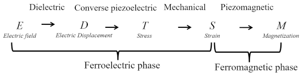
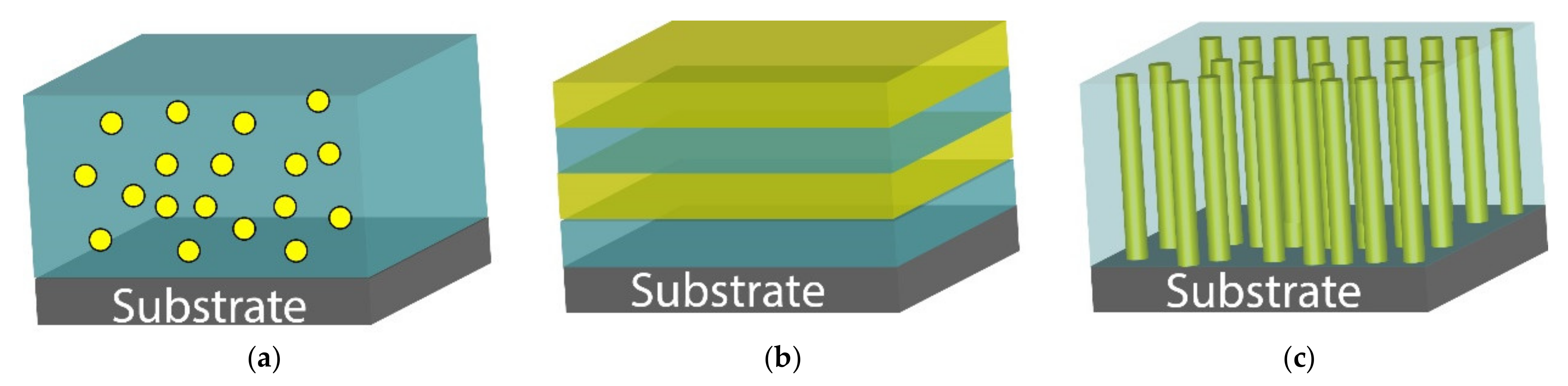
:1. Introduction

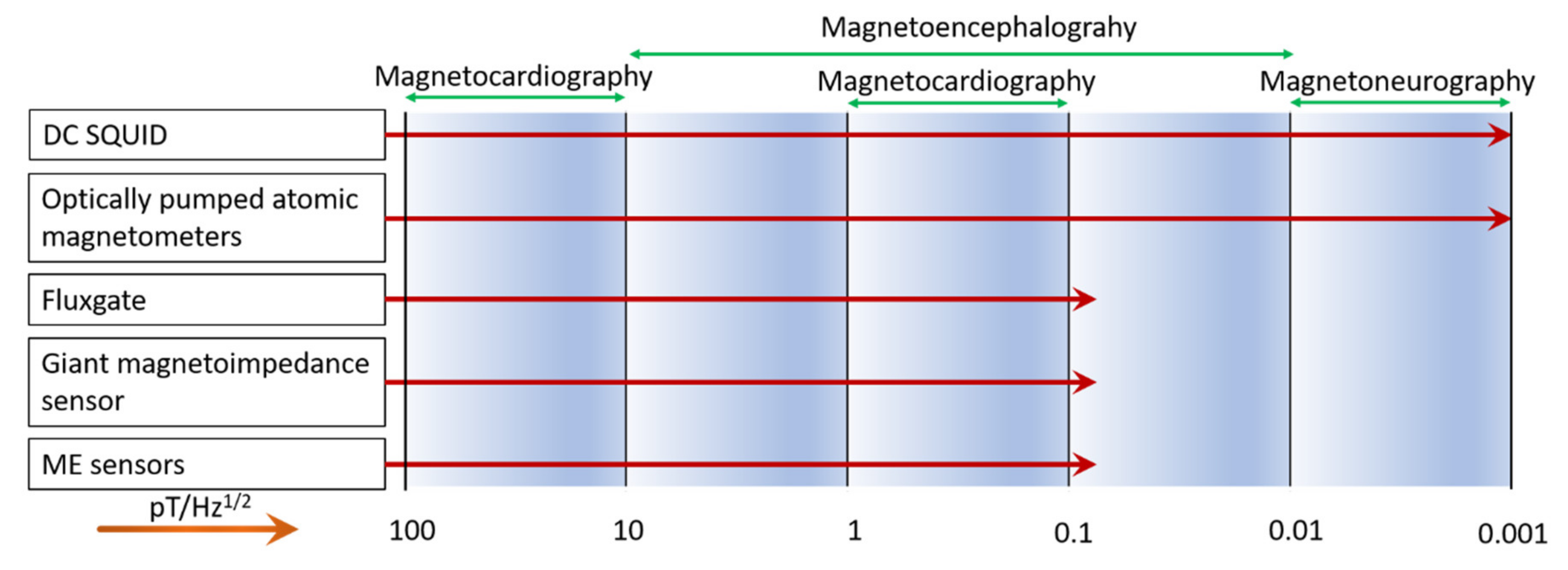
2. Thin-Film Magnetic Sensors
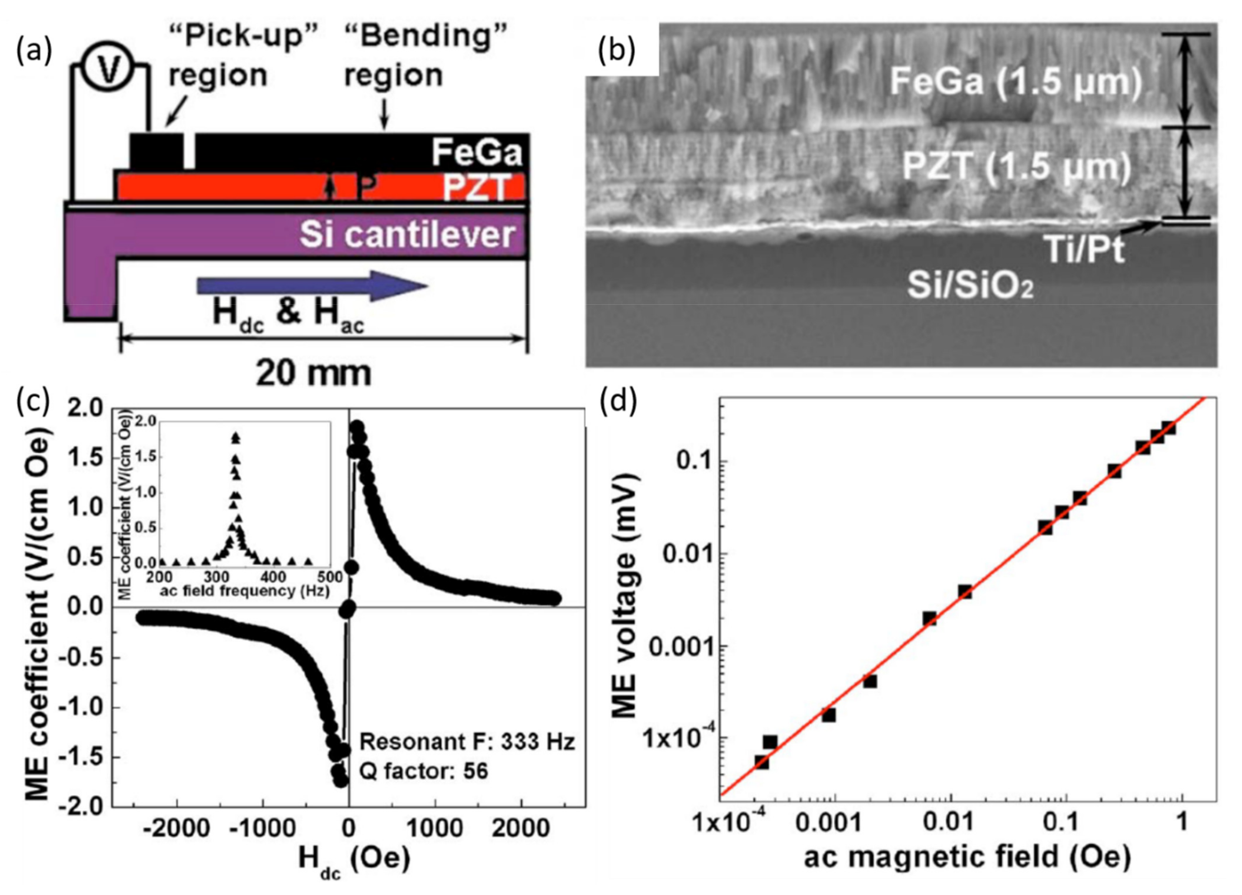
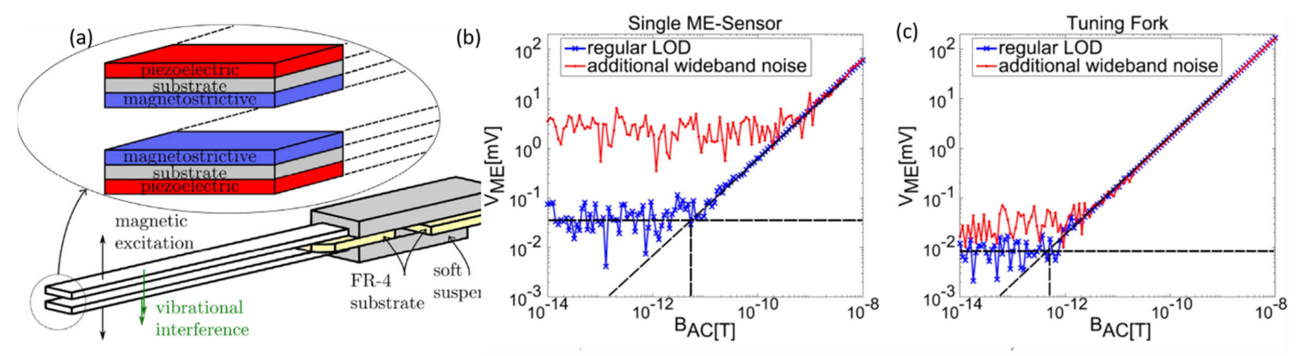
2.1. ME Cantilever Sensors
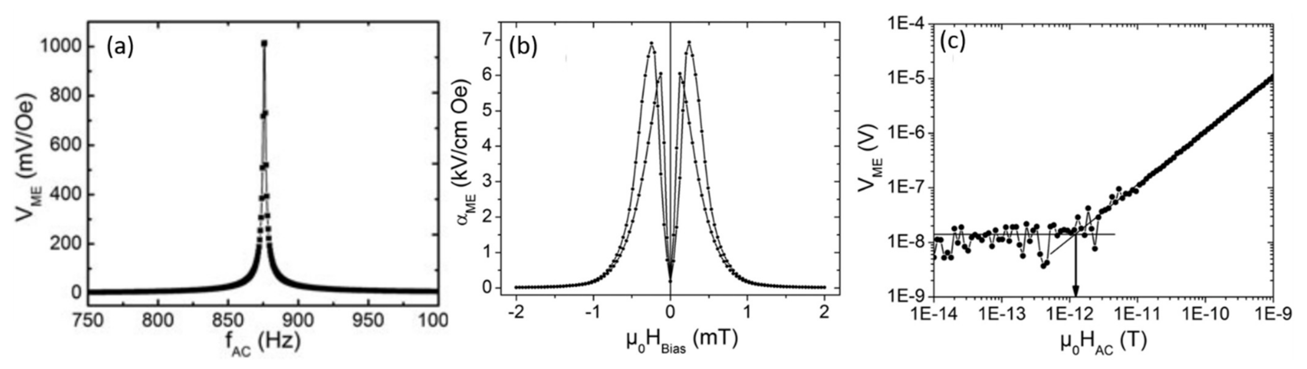
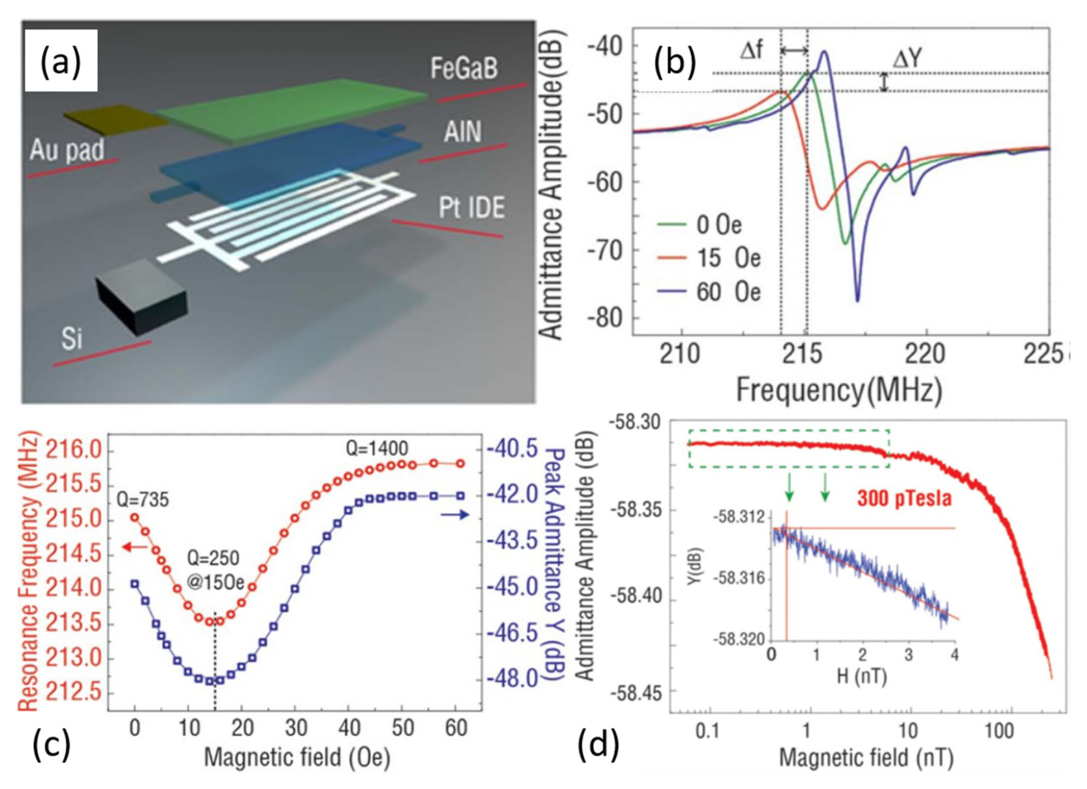
2.2. Self-Biased ME Sensors
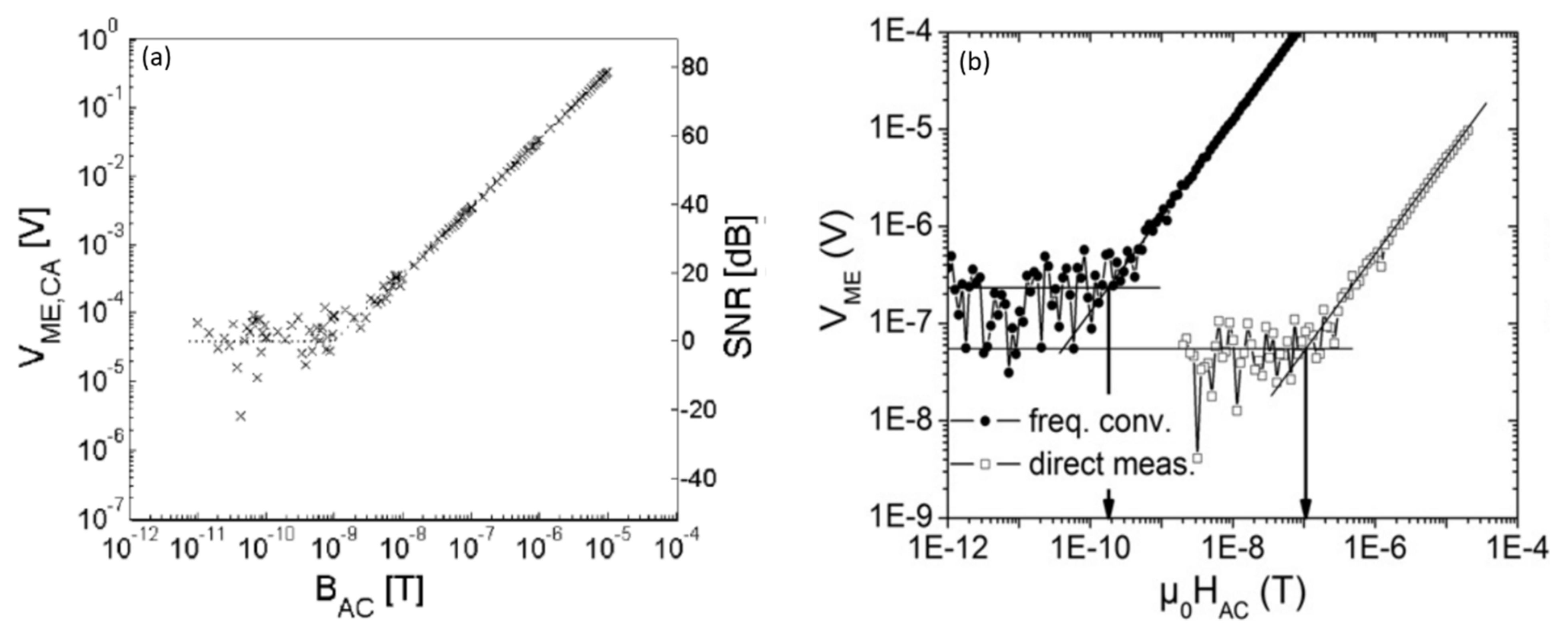
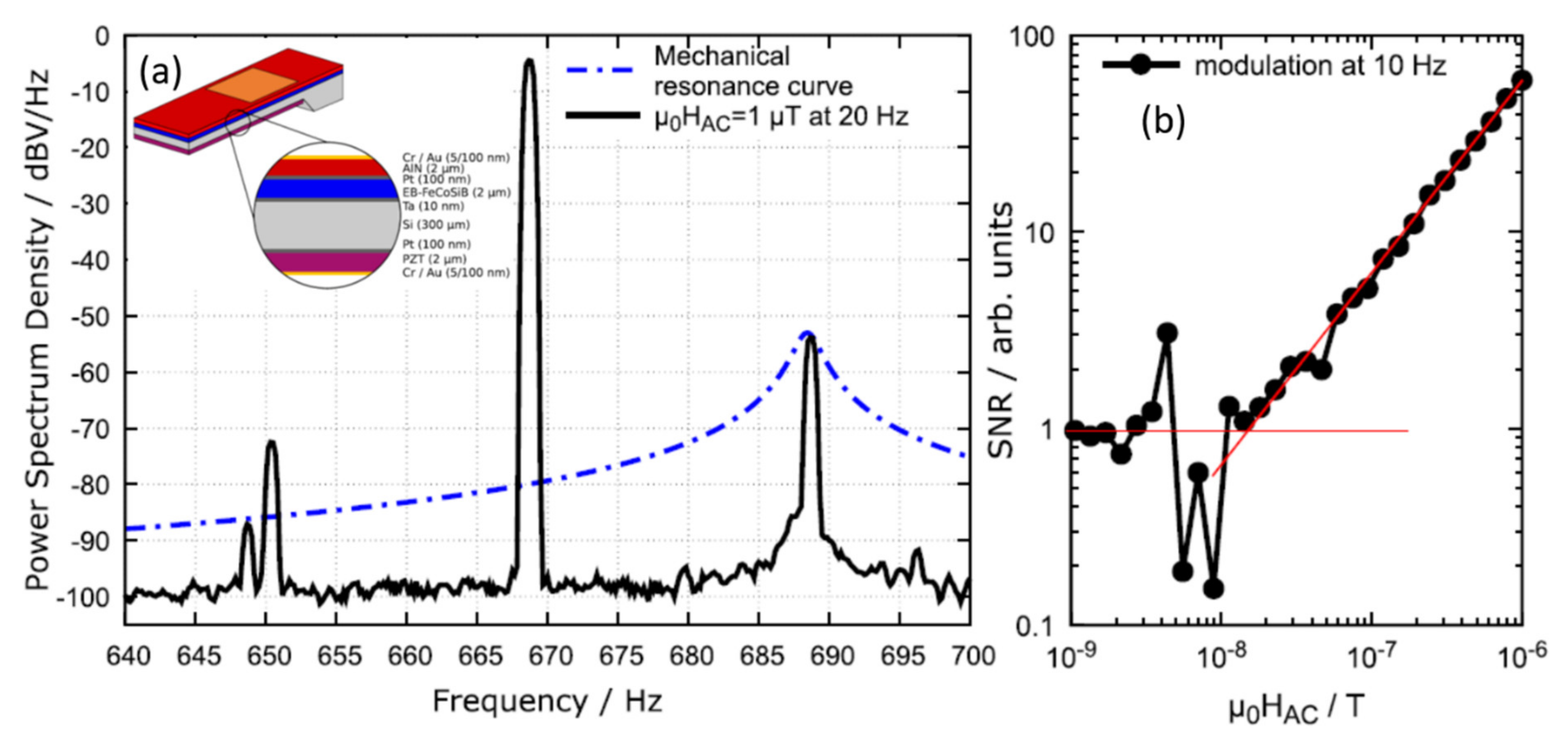
2.3. Sensitivity Enhancement of an ME Sensor Using the Frequency Conversion Technique
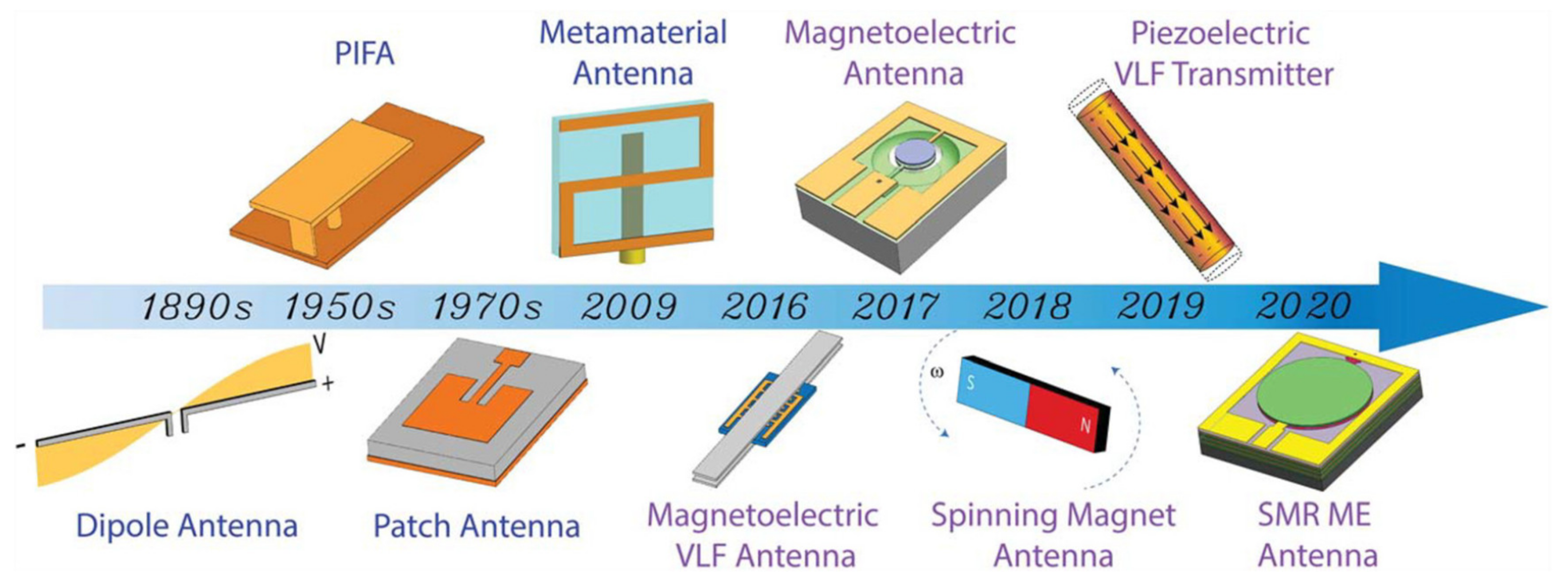
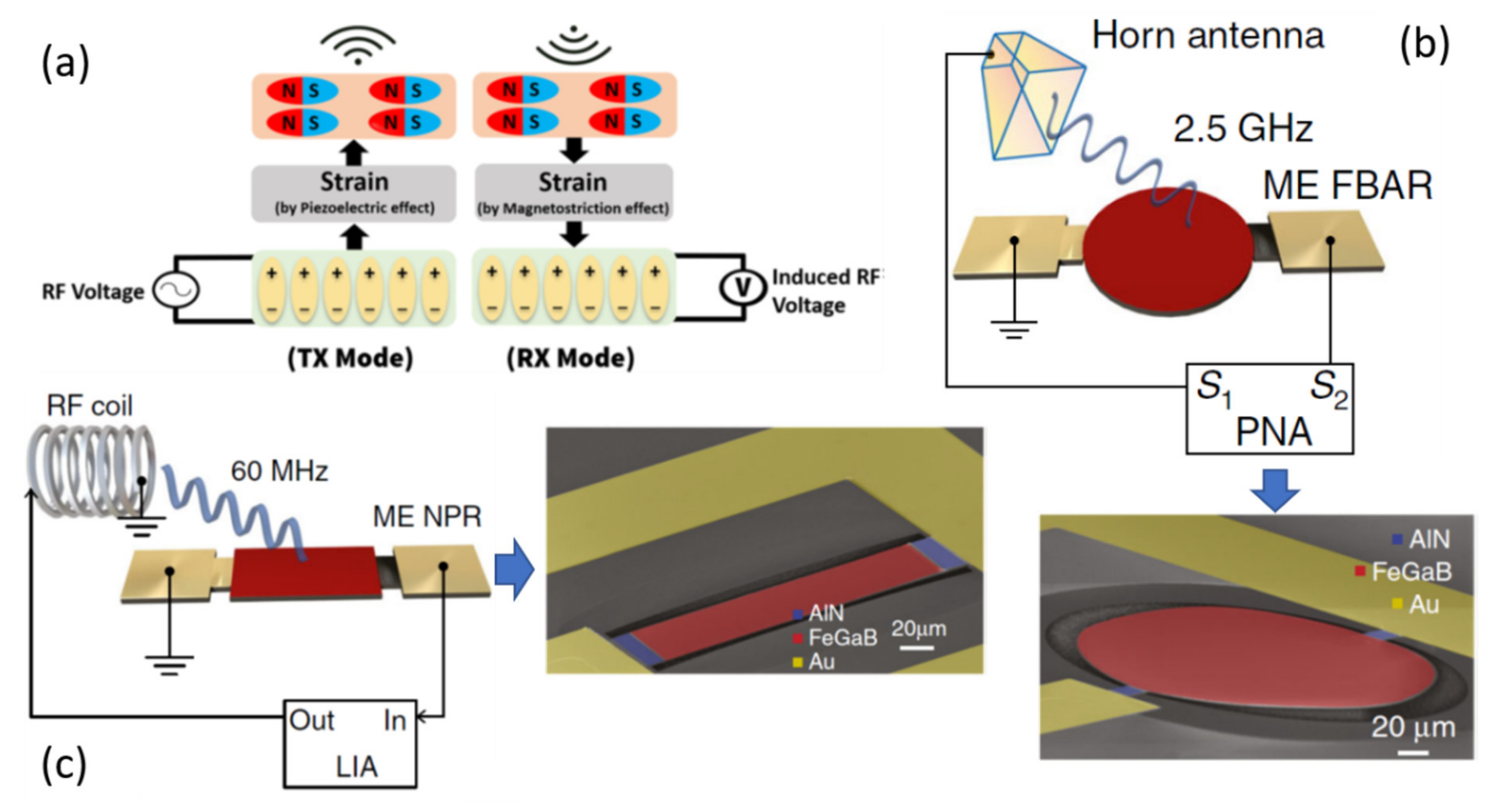
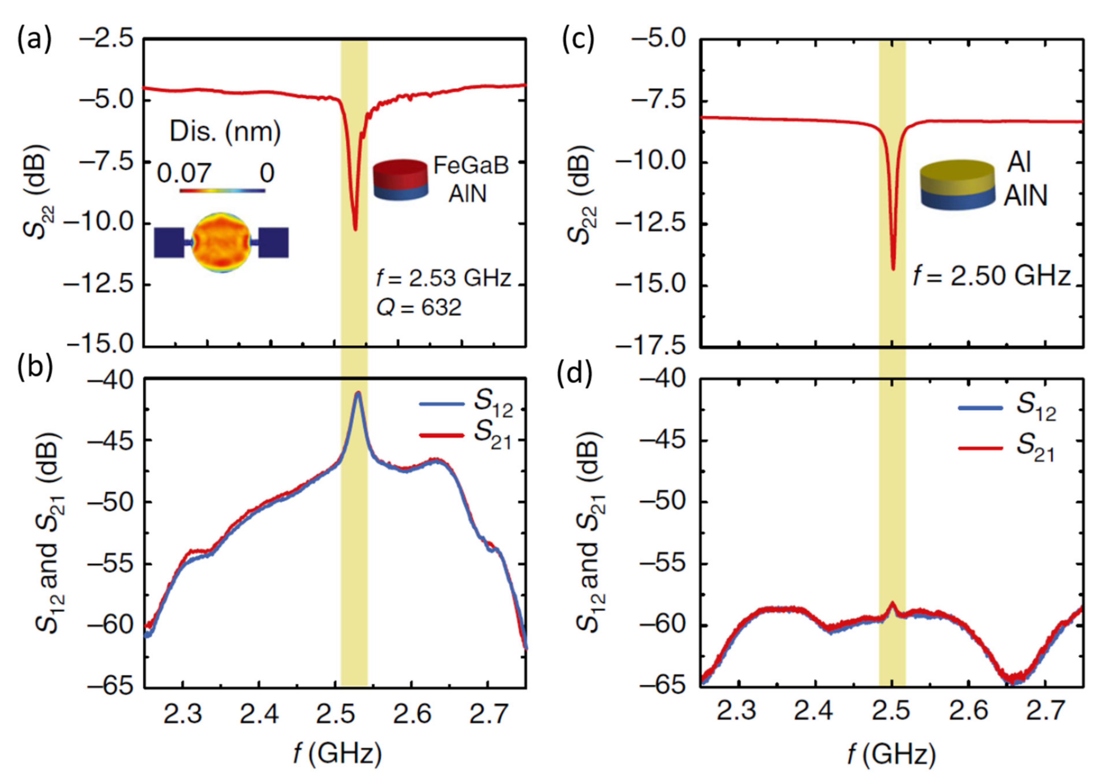
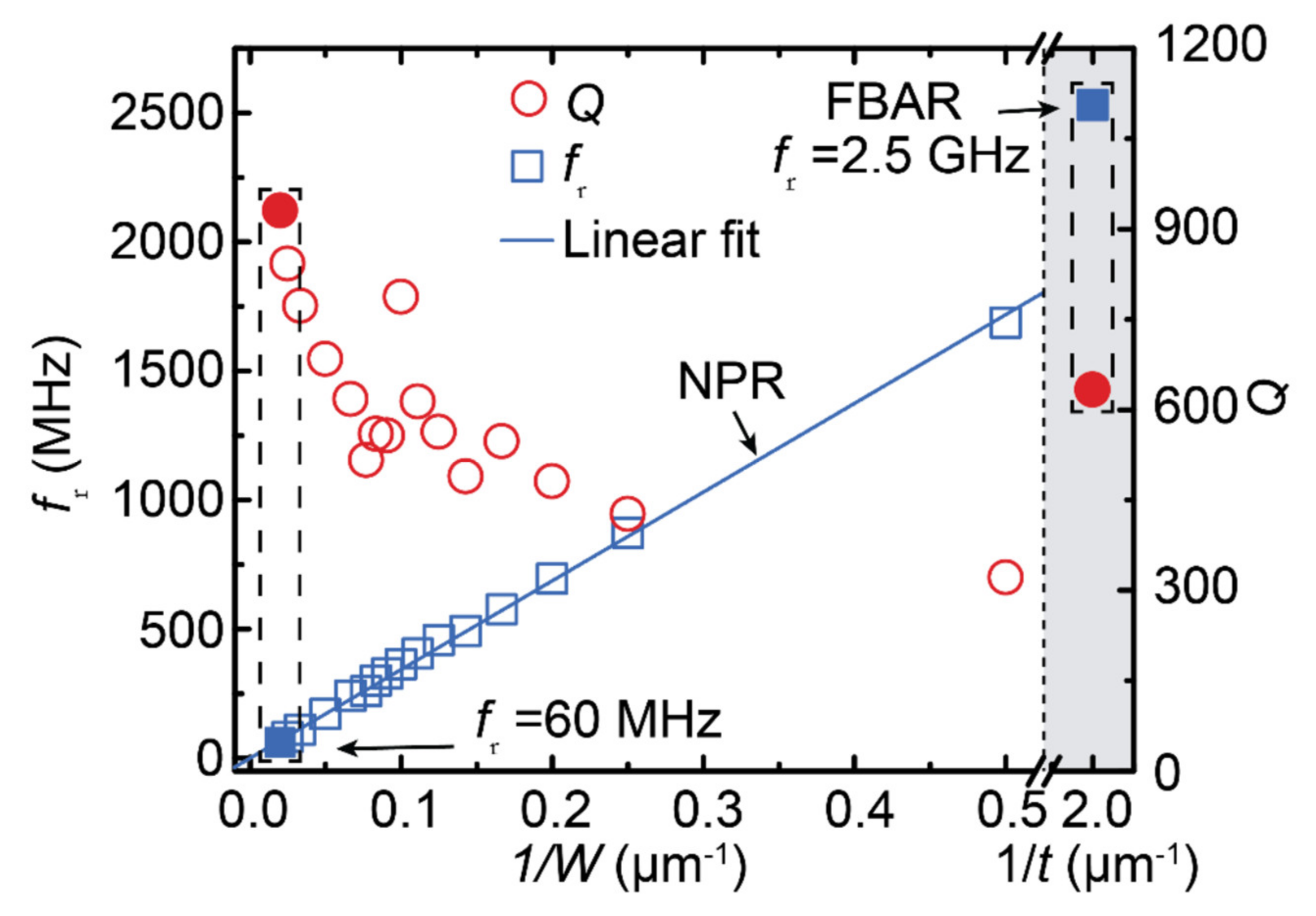
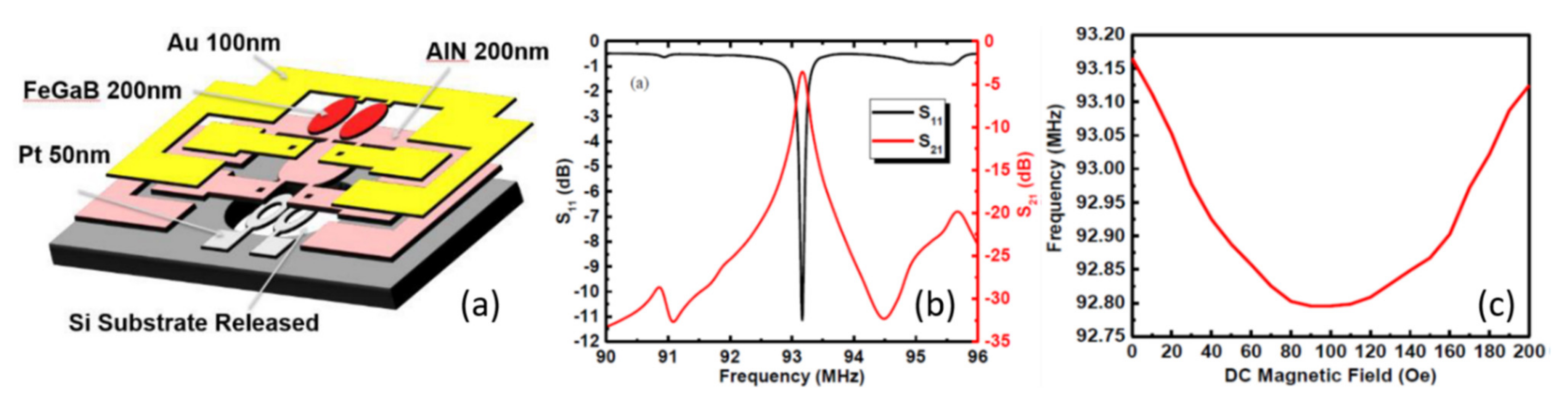
3. ME Antennas
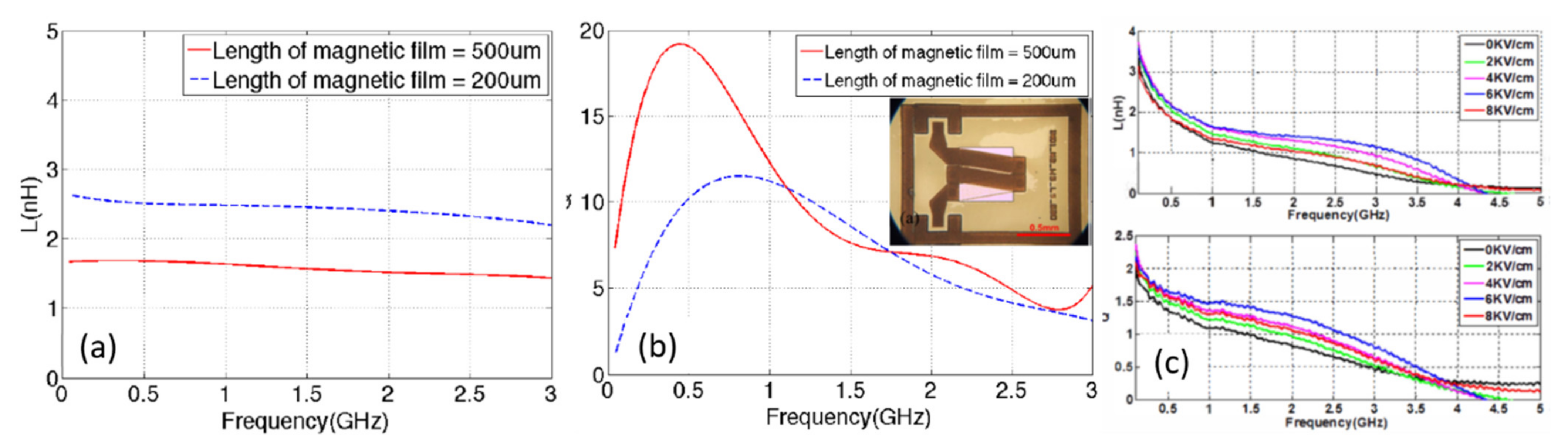
4. ME Tunable RF/Microwave Inductors
5. ME Tunable RF/Microwave Filters
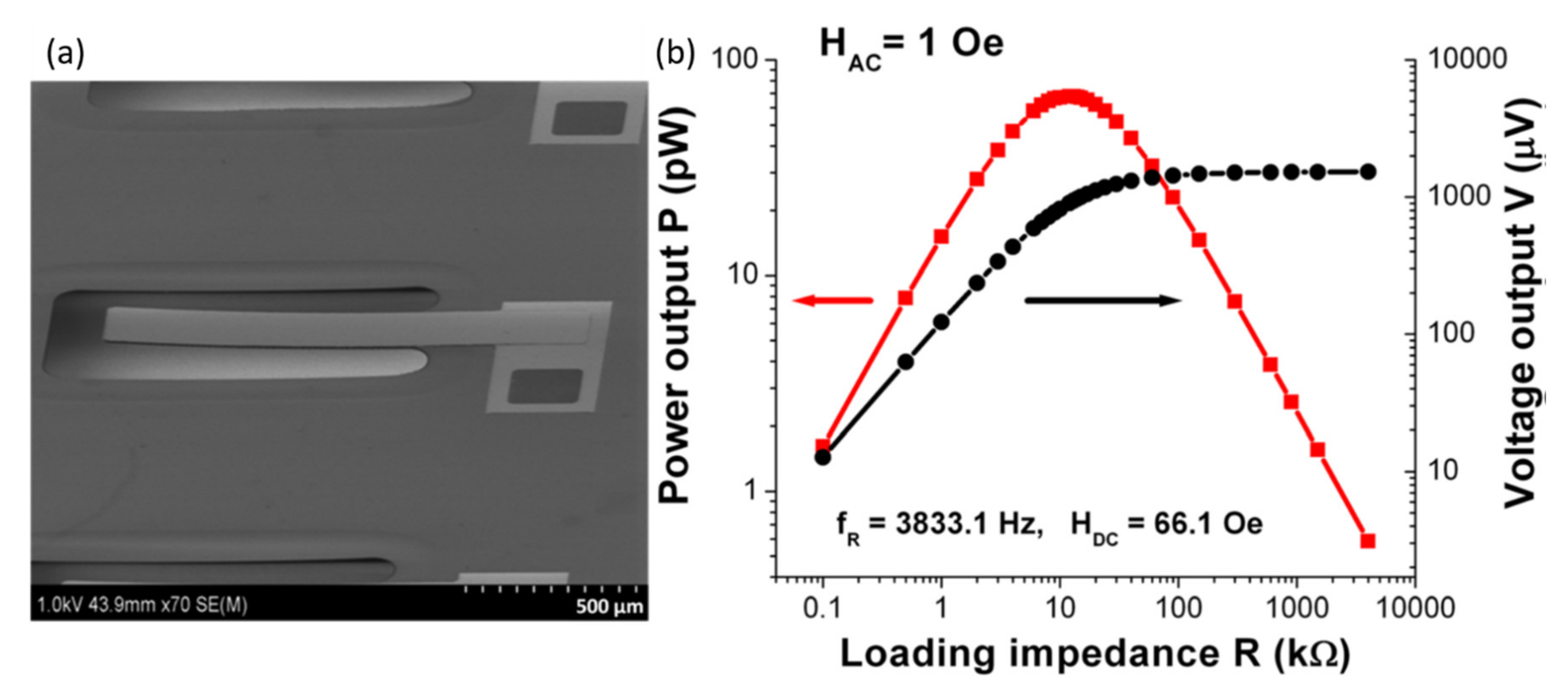
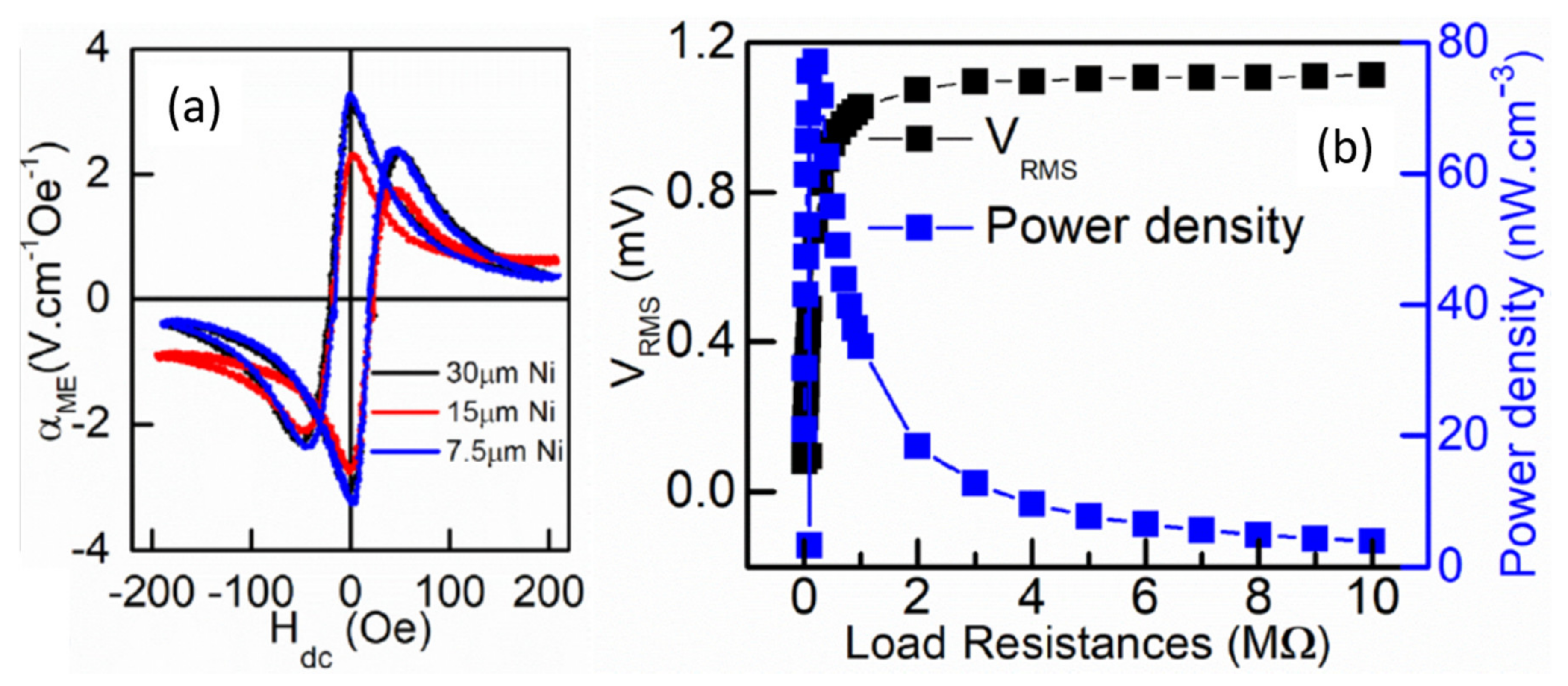
6. ME Thin Film Energy Harvesters
7. Conclusions
Author Contributions
Funding
Institutional Review Board Statement
Informed Consent Statement
Conflicts of Interest
References
- Nan, C.W.; Bichurin, M.I.; Dong, S.; Viehland, D.; Srinivasan, G. Multiferroic magnetoelectric composites: Historical perspective, status, and future directions. J. Appl. Phys. 2008, 103, 31101. [Google Scholar] [CrossRef]
- Fiebig, M. Revival of the magnetoelectric effect. J. Phys. D Appl. Phys. 2005, 38, 123. [Google Scholar] [CrossRef]
- Cho, K.H.; Priya, S. Direct and converse effect in magnetoelectric laminate composites. Appl. Phys. Lett. 2011, 98, 232904. [Google Scholar] [CrossRef] [Green Version]
- Ma, J.; Hu, J.; Li, Z.; Nan, C.W. Recent progress in multiferroic magnetoelectric composites: From bulk to thin films. Adv. Mater. 2011, 23, 1062–1087. [Google Scholar] [CrossRef] [PubMed]
- Palneedi, H.; Annapureddy, V.; Priya, S.; Ryu, J. Status and perspectives of multiferroic magnetoelectric composite materials and applications. Actuators 2016, 5, 9. [Google Scholar] [CrossRef] [Green Version]
- Suchtelen, V.J. Product properties: A new application of composite materials. Phillips Res. Rep. 1972, 27, 28–37. [Google Scholar]
- Zhou, P.; Liang, K.; Liu, Y.; Zheng, Z.; Zhang, T. Effect of interface coupling on magnetoelectric response of Pb(Zr0.52Ti0.48)-O3/La0.67Sr0.33MnO3 thin film under different strain states. Appl. Phys. A Mater. Sci. Process. 2018, 124, 670. [Google Scholar] [CrossRef]
- Zhou, P.; Singh, A.V.; Li, Z.; Popov, M.A.; Liu, Y.; Filippov, D.A.; Zhang, T.; Zhang, W.; Shah, P.J.; Howe, B.M.; et al. Magnetoelectric interactions in composites of ferrite films on lattice-matched substrates and ferroelectrics. Phys. Rev. Appl. 2019, 11, 054045. [Google Scholar] [CrossRef]
- Sahoo, S.; Polisetty, S.; Duan, C.G.; Jaswal, S.S.; Tsymbal, E.Y.; Binek, C. Ferroelectric control of magnetism in BaTiO3/Fe heterostructures via interface strain coupling. Phys. Rev. B Condens. Matter Mater. Phys. 2007, 76, 092108. [Google Scholar] [CrossRef]
- Vaz, C.A.F.; Hoffman, J.; Segal, Y.; Marshall, M.S.J.; Reiner, J.W.; Zhang, Z.; Grober, R.D.; Walker, F.J.; Ahn, C.H. Control of magnetism in Pb(Zr0.2Ti0.8)O3/La0.8Sr0.2MnO3 multiferroic heterostructures. J. Appl. Phys. 2011, 109, 07D905. [Google Scholar] [CrossRef]
- Li, N.; Liu, M.; Zhou, Z.; Sun, N.X.; Murthy, D.V.B.; Srinivasan, G.; Klein, T.M.; Petrov, V.M.; Gupta, A. Electrostatic tuning of ferromagnetic resonance and magnetoelectric interactions in ferrite-piezoelectric heterostructures grown by chemical vapor deposition. Appl. Phys. Lett. 2011, 99, 192502. [Google Scholar] [CrossRef] [Green Version]
- Cernea, M.; Vasile, B.S.; Surdu, V.A.; Trusca, R.; Bartha, C.; Craciun, F.; Galassi, C. Probing the dielectric, piezoelectric and magnetic behavior of CoFe2O4/BNT-BT0.08 composite thin film fabricated by sol-gel and spin-coating methods. Sci. Rep. 2018, 8, 17883. [Google Scholar] [CrossRef]
- Tang, Y.; Wang, R.; Zhang, Y.; Xiao, B.; Li, S.; Du, P. Magnetoelectric coupling tailored by the orientation of the nanocrystals in only one component in percolative multiferroic composites. RSC Adv. 2019, 9, 20345–20355. [Google Scholar] [CrossRef]
- El-Ghazaly, A.; Evans, J.T.; Sato, N.; Montross, N.; Ohldag, H.; White, R.M.; Wang, S.X. Electrically tunable integrated thin-film magnetoelectric resonators. Adv. Mater. Technol. 2017, 2, 1700062. [Google Scholar] [CrossRef]
- Reermann, J.; Durdaut, P.; Salzer, S.; Demming, T.; Piorra, A.; Quandt, E.; Frey, N.; Hoft, M.; Schmidt, G. Evaluation of magnetoelectric sensor systems for cardiological applications. Measurement 2018, 116, 230. [Google Scholar] [CrossRef]
- Zuo, S.; Schmalz, J.; Ozden, M.-O.; Gerken, M.; Su, J.; Niekiel, F.; Lofink, F.; Nazarpour, K. Ultrasensitive magnetoelectric sensing system for pico-Tesla magnetomyography. IEEE Trans. Biomed. Circuits Syst. 2020, 14, 971. [Google Scholar] [CrossRef] [PubMed]
- Friedrich, R.M.; Zabel, S.; Galka, A.; Lukat, N.; Wagner, J.M.; Kirchhof, C.; Quandt, E.; McCord, J.; Selhuber-Unkel, C.; Siniatchkin, M.; et al. Magnetic particle mapping using magnetoelectric sensors as an imaging modality. Sci. Rep. 2019, 9, 2086. [Google Scholar] [CrossRef] [PubMed]
- Patil, D.R.; Chai, Y.; Kambale, R.C.; Jeon, B.-G.; Yoo, K.; Ryu, J.; Yoon, W.-H.; Park, D.-S.; Jeong, D.-Y.; Lee, S.-G.; et al. Enhancement of resonant and non-resonant magnetoelectric coupling in multiferroic laminates with anisotropic piezoelectric properties. Appl. Phys. Lett. 2013, 102, 062909. [Google Scholar] [CrossRef]
- Patil, D.R.; Kambale, R.C.; Chai, Y.S.; Yoon, W.H.; Jeong, D.-Y.; Park, D.S.; Kim, J.-W.; Choi, J.-J.; Ahn, C.-W.; Hahn, B.-D.; et al. Multiple broadband magnetoelectric response in thickness-controlled Ni/[11]Pb(Mg1/3Nb2/3)O3-Pb(Zr,Ti)O3 single crystal/Ni laminates. Appl. Phys. Lett. 2013, 103, 052907. [Google Scholar] [CrossRef]
- Wang, F.; Luo, L.; Zhou, D.; Zhao, X.; Luo, H. Complete set of elastic, dielectric, and piezoelectric constants of orthorhombic 0.71Pb(Mg1∕3Nb2∕3)O3–0.29PbTiO3 single crystal. Appl. Phys. Lett. 2007, 90, 212903. [Google Scholar] [CrossRef]
- Yarar, E.; Hrkac, V.; Zamponi, C.; Piorra, A.; Kienle, L.; Quandt, E. Low temperature aluminum nitride thin films for sensory applications. AIP Adv. 2016, 6, 075115. [Google Scholar] [CrossRef]
- Fichtner, S.; Reimer, T.; Chemnitz, S.; Lofink, F.; Wagner, B. Stress controlled pulsed direct current cosputtered Al1−xScxN as piezoelectric phase for micromechanical sensor applications. APL Mater. 2015, 3, 116102. [Google Scholar] [CrossRef] [Green Version]
- Piorra, A.; Jahns, R.; Teliban, I.; Gugat, J.L.; Gerken, M.; Knöchel, R.; Quandt, E. Magnetoelectric thin film composites with interdigital electrodes. Appl. Phys. Lett. 2013, 103, 032902. [Google Scholar] [CrossRef]
- Röbisch, V.; Salzer, S.; Urs, N.O.; Reermann, J.; Yarar, E.; Piorra, A.; Kirchhof, C.; Lage, E.; Höft, M.; Schmidt, G.U. Pushing the detection limit of thin film magnetoelectric heterostructures. J. Mater. Res. 2017, 32, 1009–1019. [Google Scholar] [CrossRef]
- Viehland, D.; Wuttig, M.; McCord, J.; Quandt, Q. Magnetoelectric magnetic field sensors. MRS Bull. 2018, 43, 834–840. [Google Scholar] [CrossRef]
- Zhao, P.; Zhao, Z.; Hunter, D.; Suchoski, R.; Gao, C.; Mathews, S.; Wuttig, M.; Takeuchi, I. Fabrication and characterization of all-thin-film magnetoelectric sensors. Appl. Phys. Lett. 2009, 94, 243507. [Google Scholar] [CrossRef] [Green Version]
- Spetzler, B.; Kirchhof, C.; Quandt, E.; Mccord, J. Magnetic Sensitivity of Bending-Mode Delta-E-Effect Sensors. Phys. Rev. Appl. 2019, 12, 064036. [Google Scholar] [CrossRef]
- Röbisch, V.; Yarar, E.; Urs, N.O.; Teliban, I.; Knöchel, R.; McCord, J.; Quandt, E.; Meyners, D. Exchange biased magnetoelectric composites for magnetic field sensor application by frequency conversion. J. Appl. Phys. 2015, 117, 17B513. [Google Scholar] [CrossRef]
- Yarar, E.; Salzer, S.; Hrkac, V.; Piorra, A.; Höft, M.; Knöchel, R.; Kienle, L.; Quandt, E. Inverse bilayer magnetoelectric thin film sensor. Appl. Phys. Lett. 2016, 109, 022901. [Google Scholar] [CrossRef]
- Salzer, S.; Jahns, R.; Piorra, A.; Teliban, I.; Reermann, J.; Höft, M.; Quandt, E.; Knöchel, R. Tuning fork for noise suppression in magnetoelectric sensors. Sens. Actuators 2016, 237, 91–95. [Google Scholar] [CrossRef]
- Su, J.; Niekiel, F.; Fichtner, S.; Thormaehlen, L.; Kirchhof, C.; Meyners, D.; Quandt, E.; Wagner, B.; Lofink, F. AlScN-based MEMS Magnetoelectric Sensor. Appl. Phys. Lett. 2020, 117, 132903. [Google Scholar] [CrossRef]
- Lage, E.; Kirchhof, C.; Hrkac, V.; Kienle, L.; Jahns, R.; Knöchel, R.; Quandt, E.; Meyners, D. Exchange biasing of magnetoelectric composites. Nature 2012, 11, 523–529. [Google Scholar] [CrossRef] [PubMed]
- Jahns, R.; Zabel, S.; Marauska, S.; Gojdka, B.; Wagner, B.; Knöchel, R.; Adelung, R.; Faupel, F. Microelectromechanical magnetic field sensor based on ΔE effect. Appl. Phys. Lett. 2014, 105, 052414. [Google Scholar] [CrossRef]
- Hayes, P.; Salzer, S.; Reermann, J.; Yarar, E.; Röbisch, V.; Piorra, A.; Meyners, D.; Höft, M.; Knöchel, R.; Schmidt, G.; et al. Electrically modulated magnetoelectric sensors. Appl. Phys. Lett. 2016, 108, 182902. [Google Scholar] [CrossRef]
- Klug, M.J.; Thormahlen, L.; Robisch, V.; Toxværd, S.D.; Hoft, M.; Knochel, R.; Quandt, E.; Meyners, D.; McCord, J. Antiparallel exchange biased multilayers for low magnetic noise magnetic field sensors. J. Appl. Phys. Lett. 2019, 114, 192410. [Google Scholar] [CrossRef]
- Berry, B.S.; Pritchet, W.C. Magnetic annealing and directional ordering of an amorphous ferromagnetic alloy. Phys. Rev. Lett. 1975, 34, 1022. [Google Scholar] [CrossRef]
- Gojdka, B.; Jahns, R.; Meurisch, K.; Greve, H.; Adelung, R.; Quandt, E.; Knöchel, R.; Faupel, F. Fully integrable magnetic field sensor based on delta-E effect. Appl. Phys. Lett. 2011, 99, 223502. [Google Scholar] [CrossRef] [Green Version]
- Ngoc, N.T.; Agnus, G.; Matzen, S.; Maroutian, T.; Huong Giang, D.T.; Lecoeur, P. Cantilever magnetoelectric PZT/Tb–Fe–Co resonators for magnetic sensing applications. APL Mater. 2021, 9, 041103. [Google Scholar] [CrossRef]
- Nan, T.; Hui, Y.; Rinaldi, M.; Sun, N.X. Self-biased 215 MHz magnetoelectric NEMS resonator for ultra-sensitive DC magnetic field detection. Sci. Rep. 2013, 3, 1985. [Google Scholar] [CrossRef] [PubMed] [Green Version]
- Li, M.; Matyushov, A.; Dong, C.; Chen, H.; Lin, H.; Nan, T.; Qian, Z.; Rinaldi, M.; Lin, Y.; Sun, N.X. Ultra-sensitive NEMS magnetoelectric sensor for pico-Tesla DC magnetic field detection. Appl. Phys. Lett. 2017, 110, 143510. [Google Scholar] [CrossRef]
- Desmond, M.; Mapps, J.; Levada, K.; Belyaev, V.; Omelyanchik, A.; Panina, L.; Rodionova, V. Ultrasensitive magnetic field sensors for biomedical applications. Sensors 2020, 20, 1569. [Google Scholar]
- Chen, H.; Liang, X.; Dong, C.; He, Y.; Sun, N.; Zaeimbashi, M.; He, Y.; Gao, Y.; Parimi, P.V.; Lin, H.; et al. Ultra-compact mechanical antennas. Appl. Phys. Lett. 2020, 117, 170501. [Google Scholar] [CrossRef]
- Yao, Z.; Wang, Y.E. Bulk acoustic wave mediated multiferroic antennas near ferromagnetic resonance. In Proceedings of the 2015 IEEE International Symposium on Antennas and Propagation & USNC/URSI National Radio Science Meeting, Vancouver, BC, Canada, 19–24 July 2015. [Google Scholar] [CrossRef]
- Yao, Z.; Wang, Y.E.; Keller, S.; Carman, G.P. Bulk acoustic wavemediated multiferroic antennas: Architecture and performance bound. IEEE Trans. Antennas Propag. 2015, 63, 3335–3344. [Google Scholar] [CrossRef]
- Domann, J.P.; Carman, G.P. Strain powered antennas. J. Appl. Phys. 2016, 121, 044905. [Google Scholar] [CrossRef]
- Zaeimbashi, M.; Nasrollahpour, M.; Khalifa, A.; Romano, A.; Liang, X.; Chen, H.; Sun, N.; Matyushov, A.; Lin, H.; Dong, C.; et al. Ultra-compact dual-band smart NEMS magnetoelectric antennas for simultaneous wireless energy harvesting and magnetic field sensing. Nat. Commun. 2021, 12, 3141. [Google Scholar] [CrossRef]
- Nan, T.; Lin, H.; Gao, Y.; Matyushov, A.; Yu, G.; Chen, H.; Sun, N.; Wei, S.; Wang, Z.; Li, M.; et al. Acoustically actuated ultra-compact NEMS magnetoelectric antennas. Nat. Comm. 2017, 8, 296. [Google Scholar] [CrossRef]
- Liang, X.; Chen, H.; Sun, N.; Gao, Y.; Lin, H.; Sun, N.X. Mechanically driven SMR-based MEMS magnetoelectric antennas. In Proceedings of the 2020 IEEE International Symposium on Antennas and Propagation and North American Radio Science Meeting, Montreal, QC, Canada, 5–10 July 2020. [Google Scholar] [CrossRef]
- Lin, H.; Page, M.R.; McConney, M.; Jones, J.; Howe, B.; Sun, N.X. Integrated magnetoelectric devices: Filters, pico-Tesla magnetometers, and ultracompact acoustic antennas. MRS Bull. 2018, 43, 841–847. [Google Scholar] [CrossRef]
- Salvia, J.; Bain, J.; Yue, C. Tunable on-chip inductors up to 5 GHz using patterned permalloy laminations. In Proceedings of the IEEE InternationalElectron Devices Meeting, 2005. IEDM Technical Digest, Washington, DC, USA, 5 December 2005. [Google Scholar] [CrossRef]
- Lou, J.; Reed, D.; Liu, M.; Sun, N.X. Electrostatically tunable magnetoelectric inductors with large inductance tunability. Appl. Phys. Lett. 2009, 94, 112508. [Google Scholar] [CrossRef]
- Gao, Y.; Zardareh, S.Z.; Yang, X.; Nan, T.; Zhou, Z.Y.; Onabajo, M.; Liu, M.; Aronow, A.; Mahalingam, K.; Howe, B.M.; et al. Significantly enhanced inductance and quality factor of GHz integrated magnetic solenoid inductors with FeGaB/Al2O3 multilayer films. IEEE Trans. Electron Devices 2014, 61, 1470. [Google Scholar]
- Wu, J.; Yang, X.; Beguhn, S.; Lou, J.; Sun, N.X. Nonreciprocal tunable low-loss bandpass filters with ultra wideband isolation based on magnetostatic surface wave. IEEE Trans. Microw. Theory Tech. 2012, 60, 12. [Google Scholar] [CrossRef]
- Lin, H.; Jing, W.; Xi, Y.; Hu, Z.; Nan, T.; Emori, S.; Gao, Y.; Guo, R.; Wang, X.; Sun, N.X. Integrated non-reciprocal dual H- and E-Field tunable bandpass filter with ultra-wideband isolation. In Proceedings of the 2015 IEEE MTT-S International Microwave Symposium, Phoenix, AZ, USA, 17–22 May 2015. [Google Scholar]
- Lin, H.; Nan, T.; Qian, Z.; Gao, Y.; Hui, Y.; Wang, X.; Guo, R.; Belkessam, A.; Shi, W.; Rinaldi, M.; et al. Tunable RF band-pass filters based on NEMS magnetoelectric resonators. In Proceedings of the IEEE MTTS International Microwave Symposium, San Francisco, CA, USA, 22–27 May 2016. [Google Scholar]
- Annapureddy, V.; Kim, M.; Palneedi, H.; Lee, H.-Y.; Choi, S.-Y.; Yoon, W.-H.; Park, D.-S.; Choi, J.-J.; Hahn, B.-D.; Ahn, C.-W.; et al. Low-loss piezoelectric single-crystal fibers for enhanced magnetic energy harvesting with magnetoelectric composite. Adv. Energy Mater. 2016, 6, 1601244. [Google Scholar] [CrossRef]
- Annapureddy, V.; Lee, H.Y.; Yoon, W.H.; Woo, H.-J.; Lee, J.-H.; Palneedi, H.; Kim, H.-J.; Choi, J.-J.; Jeong, D.Y.; Yi, S.N.; et al. Enhanced magnetic energy harvesting properties of magneto-mechano-electric generator by tailored geometry. Appl. Phys. Lett. 2016, 109, 093901. [Google Scholar] [CrossRef]
- Zhang, Y.; Liu, G.; Shi, H.; Xiao, W.; Zhu, Y.; Li, M.; Liu, J. Enhanced magnetoelectric effect in ferromagnetic–elastic–piezoelectric composites. J. Alloys Compd. 2014, 613, 93–95. [Google Scholar] [CrossRef]
- Annapureddy, V.; Na, S.M.; Hwang, G.T.; Kang, M.G.; Sriramdas, R.; Palneedi, H.; Yoon, W.; Hahn, B.-D.; Kim, J.-W.; Ahn, C.-W.; et al. Exceeding milli-watt powering magneto-mechano-electric generator for standalone-powered electronics. Energy Environ. Sci. 2018, 11, 818–829. [Google Scholar] [CrossRef]
- Liu, G.; Ci, P.; Dong, S. Theoretical analysis on low frequency magneto-mechano-electric coupling behavior in piezo-unimorph/magnet composite. J. Appl. Phys. 2014, 115, 164104. [Google Scholar] [CrossRef]
- Liu, G.; Ci, P.; Dong, S. Energy harvesting from ambient low-frequency magnetic field using magneto-mechano-electric composite cantilever. Appl. Phys. Lett. 2014, 104, 032908. [Google Scholar] [CrossRef]
- Sriramdas, R.; Kang, M.G.; Meng, M.; Kiani, M.; Ryu, J.; Sanghadasa, M.; Priya, S. Large power amplification in magneto-mechano-electric harvesters through distributed forcing. Adv. Energy Mater. 2020, 10, 1903689. [Google Scholar] [CrossRef]
- Lee, H.; Sriramdas, R.; Kumar, P.; Sanghadasa, M.; Kang, M.G.; Priya, S. Maximizing power generation from ambient stray magnetic fields around smart infrastructures enabling self-powered wireless devices. Energy Environ. Sci. 2020, 13, 1462–1472. [Google Scholar] [CrossRef]
- Dong, S.; Zhai, J.; Li, J.F.; Viehland, D.; Priya, S. Multimodal system for harvesting magnetic and mechanical energy. Appl. Phys. Lett. 2008, 93, 103511. [Google Scholar] [CrossRef] [Green Version]
- Kang, M.G.; Sriramdas, R.; Lee, H.; Chun, J.; Maurya, D.; Hwang, G.T.; Ryu, J.; Priya, S. High power magnetic field energy harvesting through amplified magneto-mechanical vibration. Adv. Energy Mater. 2018, 1703313. [Google Scholar] [CrossRef]
- Liu, G.; Dong, S. A magneto-mechano-electric coupling equivalent circuit of piezoelectric bimorph/magnets composite cantilever. J. Appl. Phys. 2014, 115, 084112. [Google Scholar] [CrossRef]
- Song, H.; Patil, D.R.; Yoon, W.H.; Kim, K.H.; Choi, C.; Kim, J.H.; Hwang, G.T.; Jeong, D.Y.; Ryu, J. Significant power enhancement of magneto-mechano-electric generators by magnetic flux concentration. Energy Environ. Sci. 2020, 13, 4238–4248. [Google Scholar] [CrossRef]
- Onuta, T.D.; Wang, Y.; Long, C.J.; Takeuchi, I. Energy harvesting properties of all-thin-film multiferroic cantilevers. Appl. Phys. Lett. 2011, 99, 203506. [Google Scholar] [CrossRef] [Green Version]
- Nguyen, T.; Fleming, Y.; Bender, P.; Grysan, P. Low-temperature growth of AlN films on magnetostrictive foils for high-magnetoelectric-response thin-film composites. ACS Appl. Mater. Interfaces 2021, 13, 30874−30884. [Google Scholar] [CrossRef] [PubMed]
- Chen, H.; Liang, X.; Sun, N.; Sun, N.-X.; Lin, H.; Gao, Y. An ultra-compact ME antenna design for implantable wireless communication. In Proceedings of the 2020 IEEE International Symposium on Antennas and Propagation and North American Radio Science Meeting, Montreal, QC, Canada, 5–10 July 2020. [Google Scholar] [CrossRef]
- Liang, X.; Chen, H.; Sun, N.X. Magnetoelectric materials and devices. APL Mater. 2021, 9, 041114. [Google Scholar] [CrossRef]
- Trassin, M. Low energy consumption spintronics using multiferroic heterostructures. J. Phys. Condens. Matter 2016, 28, 033001. [Google Scholar] [CrossRef] [PubMed]
- Gradauskaite, E.; Meisenheimer, P.; Müller, M.; Heron, J.; Trassin, M. Multiferroic heterostructures for spintronics. Phys. Sci. Rev. 2020, 6, 1. [Google Scholar]


| Device | Type | ME Mechanism | Characteristics | Performance |
|---|---|---|---|---|
| ME sensor | 1. Direct sensing (a) without self-bias (b) Tuning fork (c) self-bias 2. Frequency conversion 3. Delta-E effect | DME | Highest sensitivity at fr Noise reduction Without Hdc High ME sensitivity at low frequency via MFC or EFC Change in Young modulus with the magnetic field | LoD = 135 fT/Hz1/2 at 23.23 kHz LoD = 400 fT/Hz1/2 at 867 Hz LoD = 540 pT/Hz1/2 at 10 Hz LoD = 800 pT/Hz1/2 at 10 Hz LoD = 5.1 pT/Hz1/2 at 1 Hz |
| ME antenna | VHR-NPR UHF-FBAR | DME | Width vibration mode (30–300 MHz) Width vibration mode (0.3–3 GHz) | = 6 kV/cm·Oe Gain = −18 dBi at 2.5 GHz |
| Tunable RF/Microwave devices | Tunable inductors Tunable Filters | CME DME and CME | High inductance tunability High Q at GHz Nonreciprocity | Inductance tunability = 191% Q = 19 at 0.50 GHz 5 MHz/Oe and 55 MHz/(kV/cm) |
| Energy harvesters | Magnetic field harvesting | DME | High efficiency | P = 64.61 µW |
Publisher’s Note: MDPI stays neutral with regard to jurisdictional claims in published maps and institutional affiliations. |
© 2021 by the authors. Licensee MDPI, Basel, Switzerland. This article is an open access article distributed under the terms and conditions of the Creative Commons Attribution (CC BY) license (https://creativecommons.org/licenses/by/4.0/).
Share and Cite
Patil, D.R.; Kumar, A.; Ryu, J. Recent Progress in Devices Based on Magnetoelectric Composite Thin Films. Sensors 2021, 21, 8012. https://doi.org/10.3390/s21238012
Patil DR, Kumar A, Ryu J. Recent Progress in Devices Based on Magnetoelectric Composite Thin Films. Sensors. 2021; 21(23):8012. https://doi.org/10.3390/s21238012
Chicago/Turabian StylePatil, Deepak Rajaram, Ajeet Kumar, and Jungho Ryu. 2021. "Recent Progress in Devices Based on Magnetoelectric Composite Thin Films" Sensors 21, no. 23: 8012. https://doi.org/10.3390/s21238012
APA StylePatil, D. R., Kumar, A., & Ryu, J. (2021). Recent Progress in Devices Based on Magnetoelectric Composite Thin Films. Sensors, 21(23), 8012. https://doi.org/10.3390/s21238012