
Performance Improvement of Residue-Free Graphene Field-Effect Transistor Using Au-Assisted Transfer Method

Abstract
:1. Introduction
2. Materials and Methods
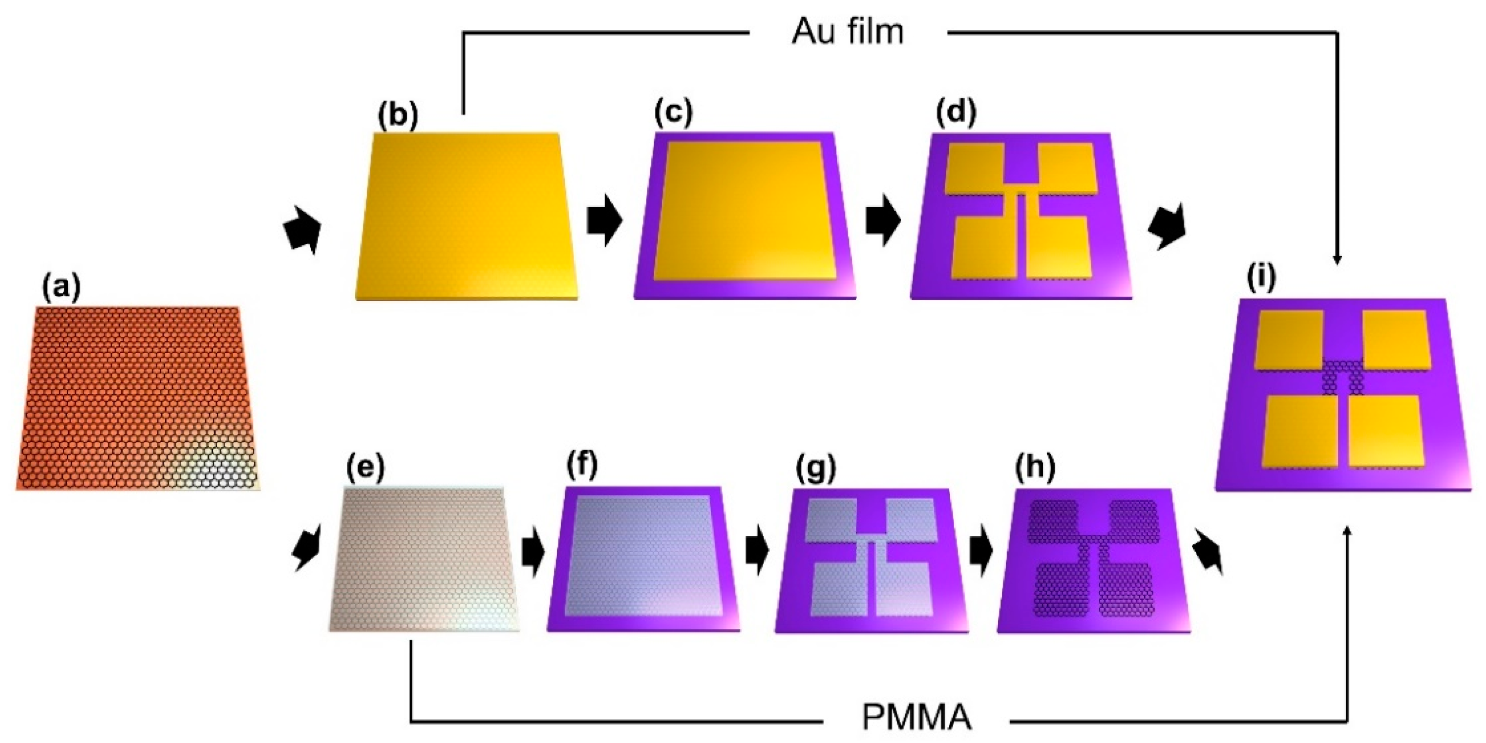
2.1. Graphene Synthesis and Transfer Process
2.2. GFET Fabrication Process
2.3. Measurement Equipment and Condition
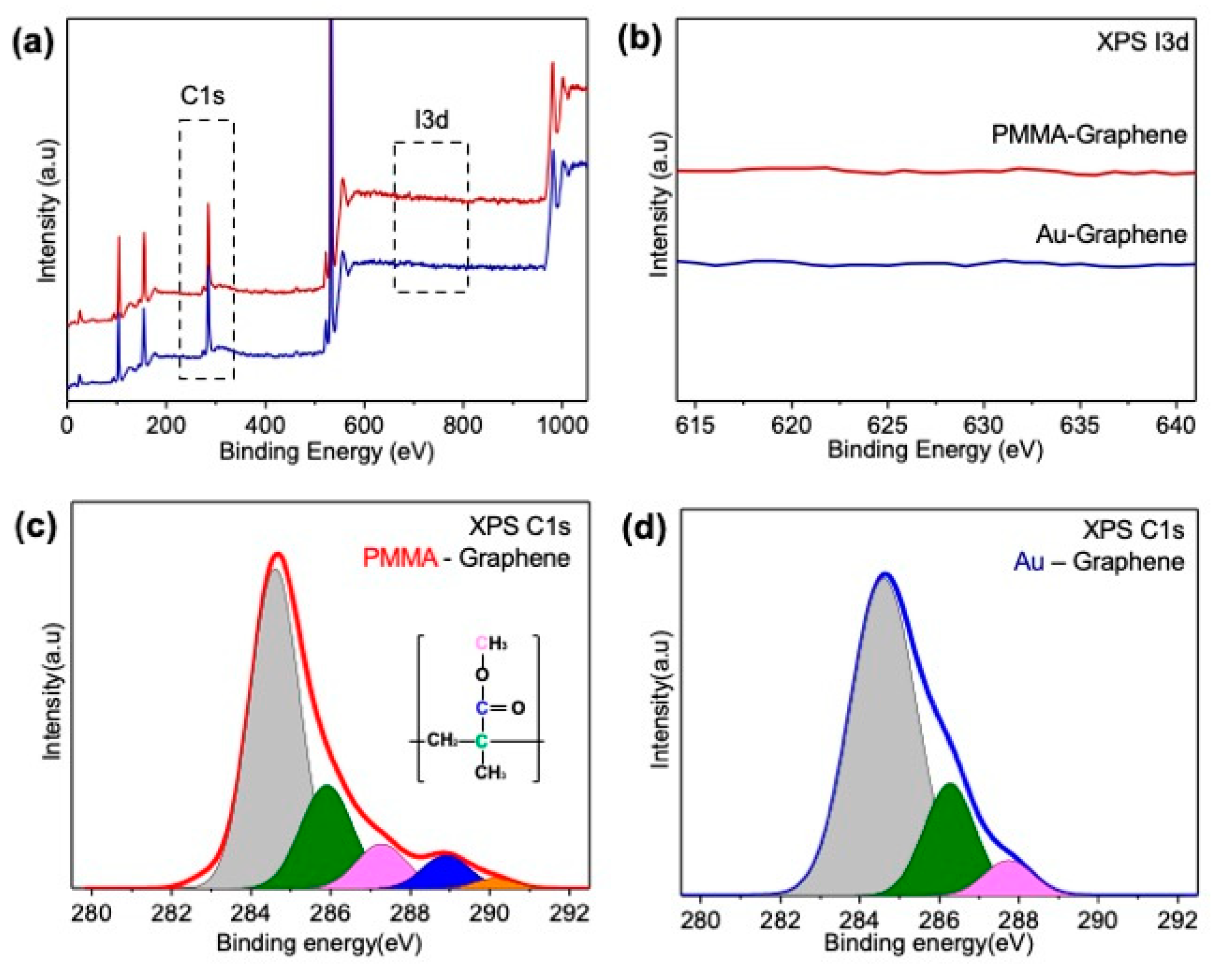
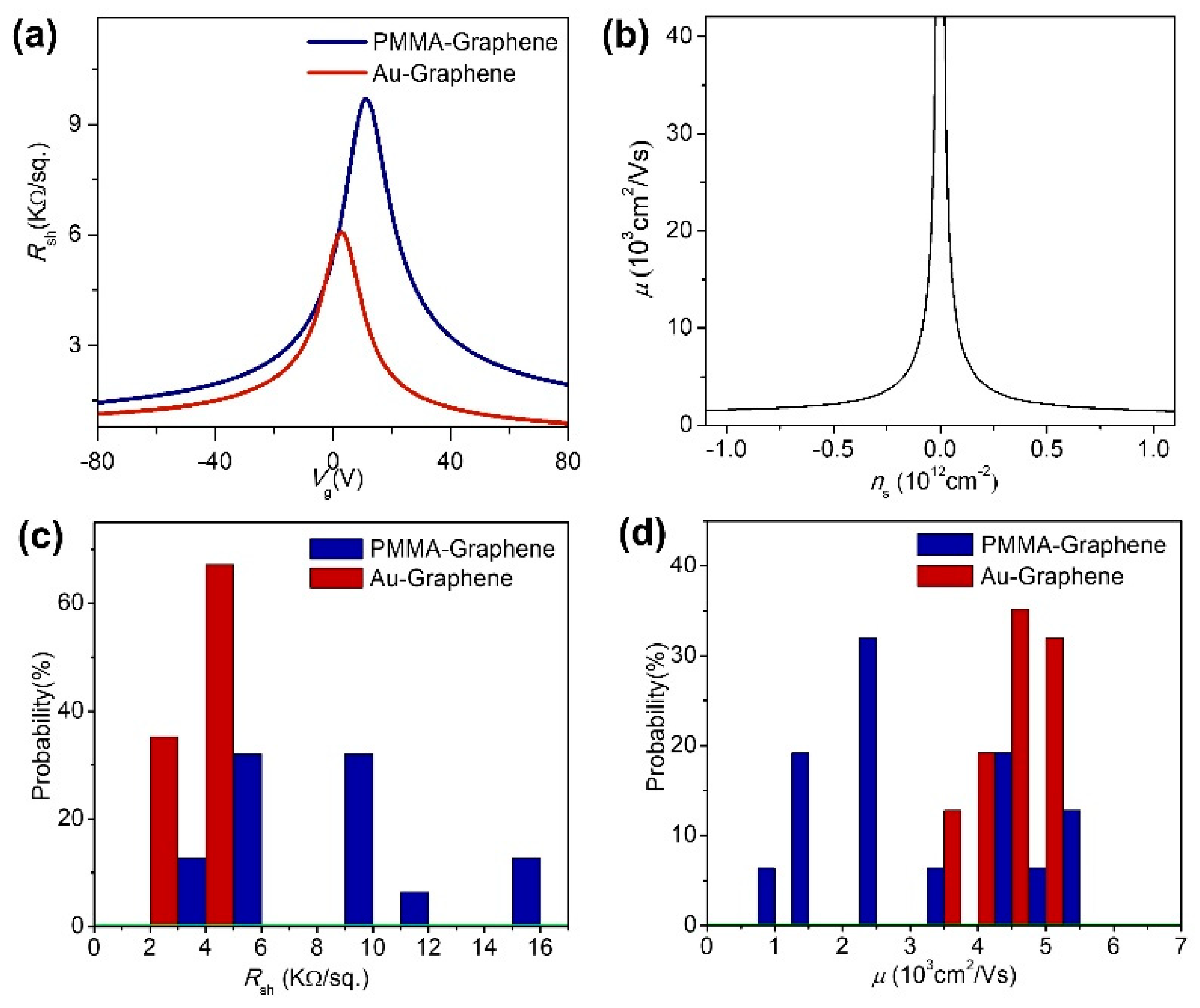
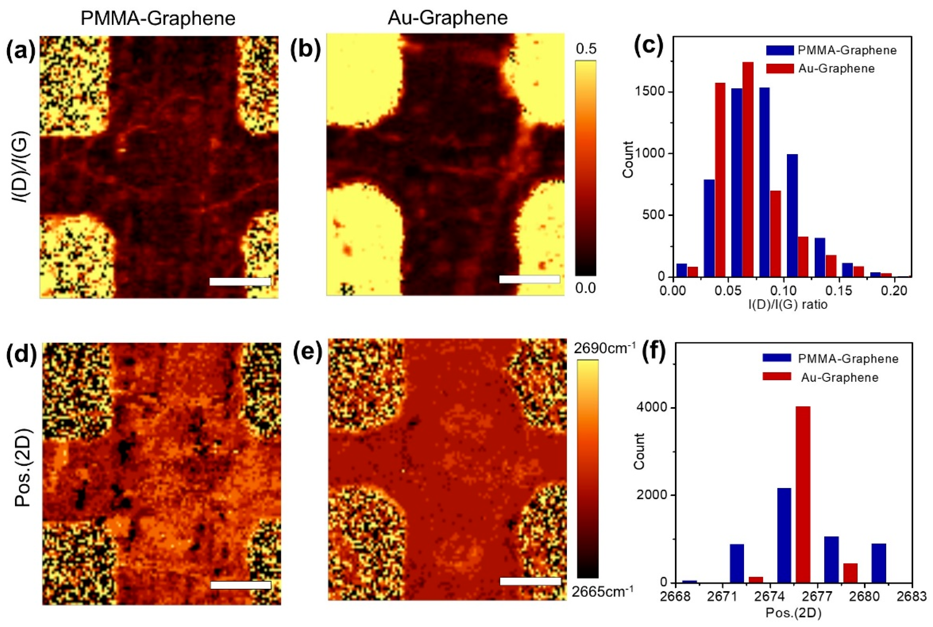
3. Results and Discussion
4. Conclusions
Supplementary Materials
Author Contributions
Funding
Institutional Review Board Statement
Informed Consent Statement
Data Availability Statement
Conflicts of Interest
References
- Novoselov, K.S.; Morozov, S.V.; Mohinddin, T.M.G.; Ponomarenko, L.A.; Elias, D.C.; Yang, R.; Barbolina, I.I.; Blake, P.; Booth, T.J.; Jiang, D.; et al. Electronic properties of graphene. Phys. Status Solidi B 2007, 244, 4106–4111. [Google Scholar] [CrossRef] [Green Version]
- Du, X.; Skachko, I.; Barker, A.; Andrei, E.Y. Approaching ballistic transport in suspended graphene. Nat. Nanotechnol. 2008, 3, 491–495. [Google Scholar] [CrossRef] [PubMed] [Green Version]
- Novoselov, K.S.; Geim, A.K.; Morozov, S.V.; Jiang, D.; Zhang, Y.; Dubonos, S.V.; Grigorieva, I.V.; Firsov, A.A. Electric field in atomically thin carbon films. Science 2004, 306, 666–669. [Google Scholar] [CrossRef] [PubMed] [Green Version]
- Mahjoub, A.M.; Motooka, S.; Aoki, N.; Song, J.; Bird, J.P.; Kawano, Y.; Ferry, D.K.; Ishibashi, K.; Ochiai, Y. Towards graphene ghz/thz nanosensor. Jpn. J. Appl. Phys. 2011, 50, 070119. [Google Scholar] [CrossRef]
- Bolotin, K.I.; Sikes, K.J.; Jiang, Z.; Klima, M.; Fudenberg, G.; Hone, J.; Kim, P.; Stormer, H.L. Ultrahigh electron mobility in suspended graphene. Solid State Commun. 2008, 146, 351–355. [Google Scholar] [CrossRef] [Green Version]
- Xia, F.; Mueller, T.; Lin, Y.; Valdes-Garcia, A.; Avouris, P. Ultrafast graphene photodetector. Nat. Nanotech. 2009, 4, 839–843. [Google Scholar] [CrossRef] [Green Version]
- Mueller, T.; Xia, F.; Avouris, P. Graphene photodetectors for high-speed optical communications. Nat. Photon. 2010, 4, 297–301. [Google Scholar] [CrossRef] [Green Version]
- Schedin, F.; Geim, A.K.; Morozov, S.V.; Hill, E.W.; Blake, P.; Katsnelson, M.I.; Novoselov, K.S. Detection of individual gas molecules adsorbed on graphene. Nat. Mater. 2007, 6, 652–655. [Google Scholar] [CrossRef]
- Pak, Y.; Kim, S.-M.; Jeong, H.; Kang, C.G.; Park, J.S.; Song, H.; Lee, R.; Myoung, N.; Lee, B.H.; Seo, S.; et al. Palladium-Decorated Hydrogen-Gas Sensors Using Periodically Aligned Graphene Nanoribbons. ACS Appl. Mater. Interfaces 2014, 6, 13293–13298. [Google Scholar] [CrossRef] [PubMed]
- De Arco, L.G.; Zhang, Y.; Schlenker, C.W.; Ryu, K.; Thompson, M.E.; Zhou, C. Continuous, Highly Flexible, and Transparent Graphene Films by Chemical Vapor Deposition for Organic Photovoltaics. ACS Nano 2010, 4, 2865–2873. [Google Scholar] [CrossRef]
- Wang, L.; Liu, W.; Zhang, Y.; Zhang, Z.-H.; Tiam Tan, S.; Yi, X.; Wang, G.; Sun, X.; Zhu, H.; Demir, H.V. Graphene-based transparent conductive electrodes for GaN-based light emitting diodes: Challenges and countermeasures. Nano Energy 2015, 12, 419–436. [Google Scholar] [CrossRef]
- Berger, C.; Song, Z.; Li, X.; Wu, X.; Brown, N.; Naud, C.; Mayou, D.; Li, T.; Hass, J.; Marchenkov, A.N.; et al. Electronic confinement and coherence in patterned epitaxial graphene. Science 2006, 312, 1191–1196. [Google Scholar] [CrossRef] [PubMed] [Green Version]
- Kosynkin, D.V.; Higginbotham, A.L.; Sinitskii, A.; Lomeda, J.R.; Dimiev, A.; Price, B.K.; Tour, J.M. Longitudinal unzipping of carbon nanotubes to form graphene nanoribbons. Nature 2009, 458, 872–876. [Google Scholar] [CrossRef] [Green Version]
- Li, D.; Müller, M.B.; Gilje, S.; Kaner, R.B.; Wallace, G.G. Processable aqueous dispersions of graphene nanosheets. Nat. Nanotechnol. 2008, 3, 101–105. [Google Scholar] [CrossRef]
- Li, X.; Cai, W.; An, J.; Kim, S.; Nah, J.; Yang, D.; Piner, R.; Velamakanni, A.; Jung, I.; Tutuc, E.; et al. Large-area synthesis of high-quality and uniform graphene films on copper foils. Science 2009, 324, 1312–1314. [Google Scholar] [CrossRef] [PubMed] [Green Version]
- Kim, K.S.; Zhao, Y.; Jang, H.; Lee, S.Y.; Kim, J.M.; Kim, K.S.; Ahn, J.H.; Kim, P.; Choi, J.Y.; Hong, B.H. Large-scale pattern growth of graphene films for stretchable transparent electrodes. Nature 2009, 457, 706–710. [Google Scholar] [CrossRef] [PubMed]
- Liao, Z.M.; Han, B.H.; Zhou, Y.B.; Yu, D.P. Hysteresis reversion in graphene field-effect transistors. J. Chem. Phys. 2010, 133, 044703. [Google Scholar] [CrossRef]
- Liu, W.; Li, H.; Xu, C.; Khatami, Y.; Banerjee, K. Synthesis of high-quality monolayer and bilayer graphene on copper using chemical vapor deposition. Carbon 2011, 49, 4122–4130. [Google Scholar] [CrossRef]
- Huang, P.Y.; Ruiz-Vargas, C.S.; Van Der Zande, A.M.; Whitney, W.S.; Levendorf, M.P.; Kevek, J.W.; Garg, S.; Alden, J.S.; Hustedt, C.J.; Zhu, Y.; et al. Grains and grain boundaries in single-layer graphene atomic patchwork quilts. Nature 2011, 469, 389–392. [Google Scholar] [CrossRef] [Green Version]
- Li, X.; Magnuson, C.W.; Venugopal, A.; Tromp, R.M.; Hannon, J.B.; Vogel, E.M.; Colombo, L.; Ruoff, R.S. Large-area graphene single crystals grown by low-pressure chemical vapor deposition of methane on copper. J. Am. Chem. Soc. 2011, 133, 2816–2819. [Google Scholar] [CrossRef]
- Chen, S.; Ji, H.; Chou, H.; Li, Q.; Li, H.; Suk, J.W.; Piner, R.; Liao, L.; Cai, W.; Ruoff, R.S. Millimeter-size single-crystal graphene by suppressing evaporative loss of Cu during low pressure chemical vapor deposition. Adv. Mater. 2013, 25, 2062–2065. [Google Scholar] [CrossRef] [PubMed]
- Pirkle, A.; Chan, J.; Venugopal, A.; Hinojos, D.; Magnuson, C.W.; McDonnell, S.; Colombo, L.; Vogel, E.M.; Ruoff, R.S.; Wallace, R.M. The effect of chemical residues on the physical and electrical properties of chemical vapor deposited graphene transferred to SiO2. Appl. Phys. Lett. 2011, 99, 122108. [Google Scholar] [CrossRef] [Green Version]
- Wood, J.D.; Doidge, G.P.; Carrion, E.A.; Koepke, J.C.; Kaitz, J.A.; Datye, I.; Behnam, A.; Hewaparakrama, J.; Aruin, B.; Chen, Y.; et al. Annealing free, clean graphene transfer using alternative polymer scaffolds. Nanotechnology 2015, 26, 055302. [Google Scholar] [CrossRef] [PubMed] [Green Version]
- Goniszewski, S.; Adabi, M.; Shaforost, O.; Hanham, S.M.; Hao, L.; Klein, N. Correlation of p-doping in CVD Graphene with Substrate Surface Charges. Sci. Rep. 2016, 6, 22858. [Google Scholar] [CrossRef]
- Dan, Y.; Lu, Y.; Kybert, N.J.; Luo, Z.; Johnson, A.T.C. Intrinsic response of graphene vapor sensors. Nano Lett. 2009, 9, 1472–1475. [Google Scholar] [CrossRef] [Green Version]
- Alyobi, M.M.M.; Barnett, C.J.; Cobley, R.J. Effects of Thermal Annealing on the Properties of Mechanically Exfoliated Suspended and On-Substrate Few-Layer Graphene. Crystals 2017, 7, 349. [Google Scholar] [CrossRef] [Green Version]
- Ahn, Y.; Kim, H.; Kim, Y.H.; Yi, Y.; Kim, S.I. Procedure of removing polymer residues and its influences on electronic and structural characteristics of graphene. Appl. Phys. Lett. 2013, 102, 091602. [Google Scholar] [CrossRef]
- Lin, Y.C.; Lu, C.C.; Yeh, C.H.; Jin, C.; Suenaga, K.; Chiu, P.W. Graphene annealing: How clean can it be? Nano Lett. 2012, 12, 414–419. [Google Scholar] [CrossRef] [PubMed]
- Lin, Y.C.; Jin, C.; Lee, J.C.; Jen, S.F.; Suenaga, K.; Chiu, P.W. Clean transfer of graphene for isolation and suspension. ACS Nano 2011, 5, 2362–2368. [Google Scholar] [CrossRef]
- Cheng, Z.; Zhou, Q.; Wang, C.; Li, Q.; Wang, C.; Fang, Y. Toward intrinsic graphene surfaces: A systematic study on thermal annealing and wet-chemical treatment of SiO2-supported graphene devices. Nano Lett. 2011, 11, 767–771. [Google Scholar] [CrossRef] [PubMed]
- Levendorf, M.P.; Ruiz-Vargas, C.S.; Garg, S.; Park, J. Transfer-free batch fabrication of single layer graphene transistors. Nano Lett. 2009, 9, 4479–4483. [Google Scholar] [CrossRef]
- Wang, D.Y.; Huang, I.S.; Ho, P.H.; Li, S.S.; Yeh, Y.C.; Wang, D.W.; Chen, W.L.; Lee, Y.Y.; Chang, Y.M.; Chen, C.C.; et al. Clean-lifting transfer of large-area residual-free graphene films. Adv. Mater. 2013, 25, 4521–4526. [Google Scholar] [CrossRef]
- Reina, A.; Jia, X.; Ho, J.; Nezich, D.; Son, H.; Bulovic, V.; Dresselhaus, M.S.; Jing, K. Large area, few-layer graphene films on arbitrary substrates by chemical vapor deposition. Nano Lett. 2009, 9, 30–35. [Google Scholar] [CrossRef] [PubMed]
- Lee, J.; Kim, Y.; Shin, H.-J.; Lee, C.; Lee, D.; Moon, C.-Y.; Lim, J.; Jun, S.C. Clean transfer of graphene and its effect on contact resistance. Appl. Phys. Lett. 2013, 103, 103104–103105. [Google Scholar] [CrossRef]
- Kalita, G.; Wakita, K.; Takahashi, M.; Umeno, M. Lodine doping in solid precursor-based CVD growth graphene film. J. Mater. Chem. 2011, 21, 15209–15213. [Google Scholar] [CrossRef]
- Fangping, O.; Huang, B.; Li, Z.; Xiao, J.; Wang, H.; Xu, H. Chemical functionalization of graphene nanoribbons by carboxyl groups on stone-wales defects. J. Phys. Chem. C 2008, 112, 12003–12007. [Google Scholar]
- Hong, S.K.; Song, S.M.; Sul, O.; Cho, B.J. Carboxylic group as the origin of electrical performance degradation during the transfer process of CVD growth graphene. J. Electrochem. Soc. 2012, 159, K107–K109. [Google Scholar] [CrossRef]
- Mitta, S.B.; Choi, M.S.; Nipane, A.; Ali, F.; Kim, C.; Teherani, J.T.; Hone, J.; Yoo, W.J. Electrical characterization of 2D materials-based field-effect transistors. 2D Mater. 2020, 8, 012002. [Google Scholar] [CrossRef]
- Venugopal, A.; Colombo, L.; Vogel, E.M. Issues with characterizing transport properties of graphene field effect transistors. Solid State Commun. 2012, 152, 1311–1316. [Google Scholar] [CrossRef]
- Suk, J.W.; Lee, W.H.; Lee, J.; Chou, H.; Piner, R.D.; Hao, Y.; Akinwande, D.; Ruoff, R.S. Enhancement of the electrical properties of graphene grown by chemical vapor deposition via controlling the effects of polymer residue. Nano Lett. 2013, 13, 1462–1467. [Google Scholar] [CrossRef]
- Ferrari, A.C. Raman spectroscopy of graphene and graphite: Disorder, electron-phonon coupling, doping and nonadiabatic effects. Solid State Commun. 2007, 143, 47–57. [Google Scholar] [CrossRef]
- Lucchese, M.M.; Stavale, F.; Ferreira, E.H.M.; Vilani, C.; Moutinho, M.V.O.; Capaz, R.B.; Achete, C.A.; Jorio, A. Quantifying ion-induced defects and Raman relaxation length in graphene. Carbon 2010, 48, 1592–1597. [Google Scholar] [CrossRef]


Publisher’s Note: MDPI stays neutral with regard to jurisdictional claims in published maps and institutional affiliations. |
© 2021 by the authors. Licensee MDPI, Basel, Switzerland. This article is an open access article distributed under the terms and conditions of the Creative Commons Attribution (CC BY) license (https://creativecommons.org/licenses/by/4.0/).
Share and Cite
Jang, Y.; Seo, Y.-M.; Jang, H.-S.; Heo, K.; Whang, D. Performance Improvement of Residue-Free Graphene Field-Effect Transistor Using Au-Assisted Transfer Method. Sensors 2021, 21, 7262. https://doi.org/10.3390/s21217262
Jang Y, Seo Y-M, Jang H-S, Heo K, Whang D. Performance Improvement of Residue-Free Graphene Field-Effect Transistor Using Au-Assisted Transfer Method. Sensors. 2021; 21(21):7262. https://doi.org/10.3390/s21217262
Chicago/Turabian StyleJang, Yamujin, Young-Min Seo, Hyeon-Sik Jang, Keun Heo, and Dongmok Whang. 2021. "Performance Improvement of Residue-Free Graphene Field-Effect Transistor Using Au-Assisted Transfer Method" Sensors 21, no. 21: 7262. https://doi.org/10.3390/s21217262
APA StyleJang, Y., Seo, Y.-M., Jang, H.-S., Heo, K., & Whang, D. (2021). Performance Improvement of Residue-Free Graphene Field-Effect Transistor Using Au-Assisted Transfer Method. Sensors, 21(21), 7262. https://doi.org/10.3390/s21217262