
Process Variability in Top-Down Fabrication of Silicon Nanowire-Based Biosensor Arrays


Abstract
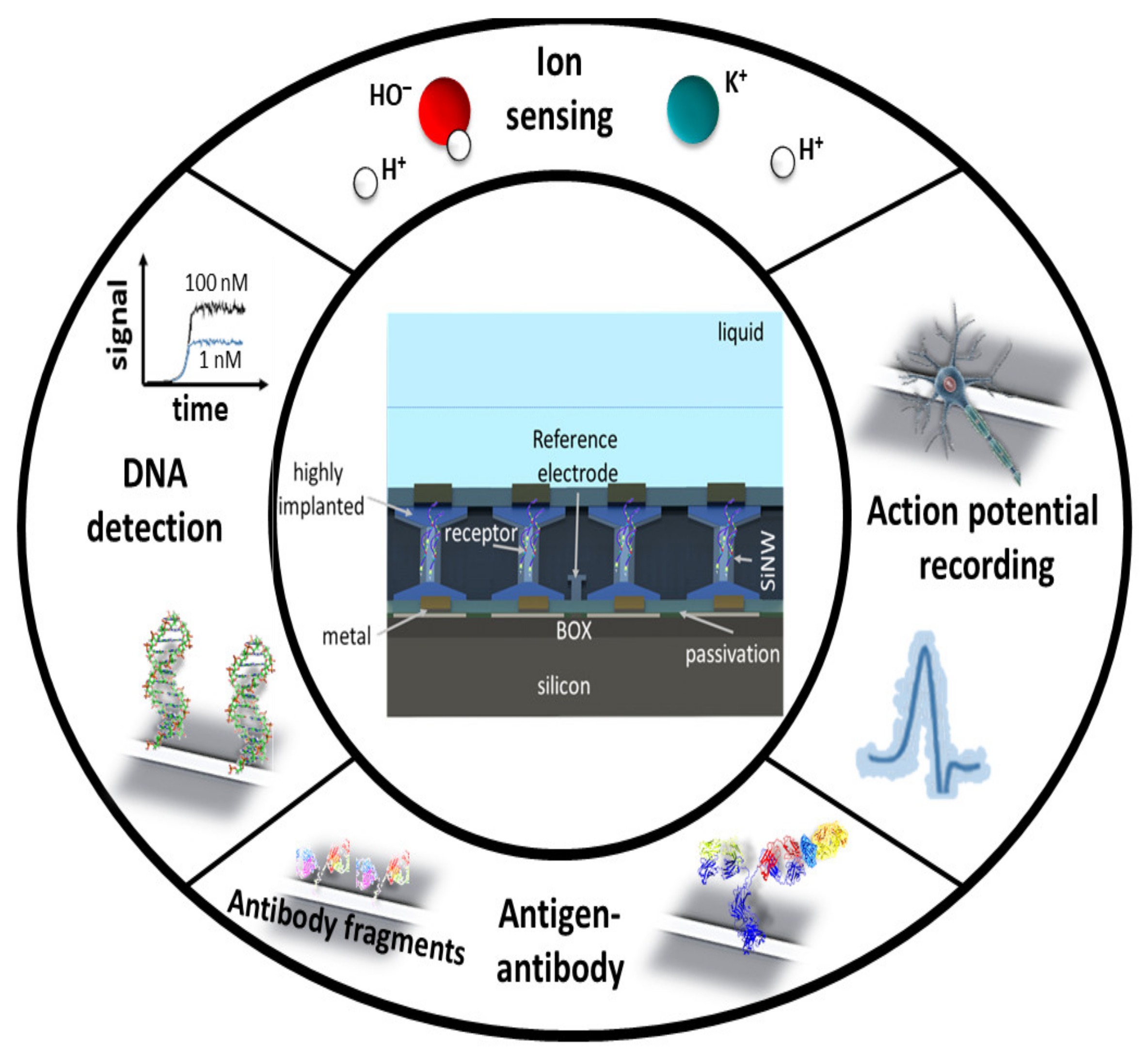
1. Introduction
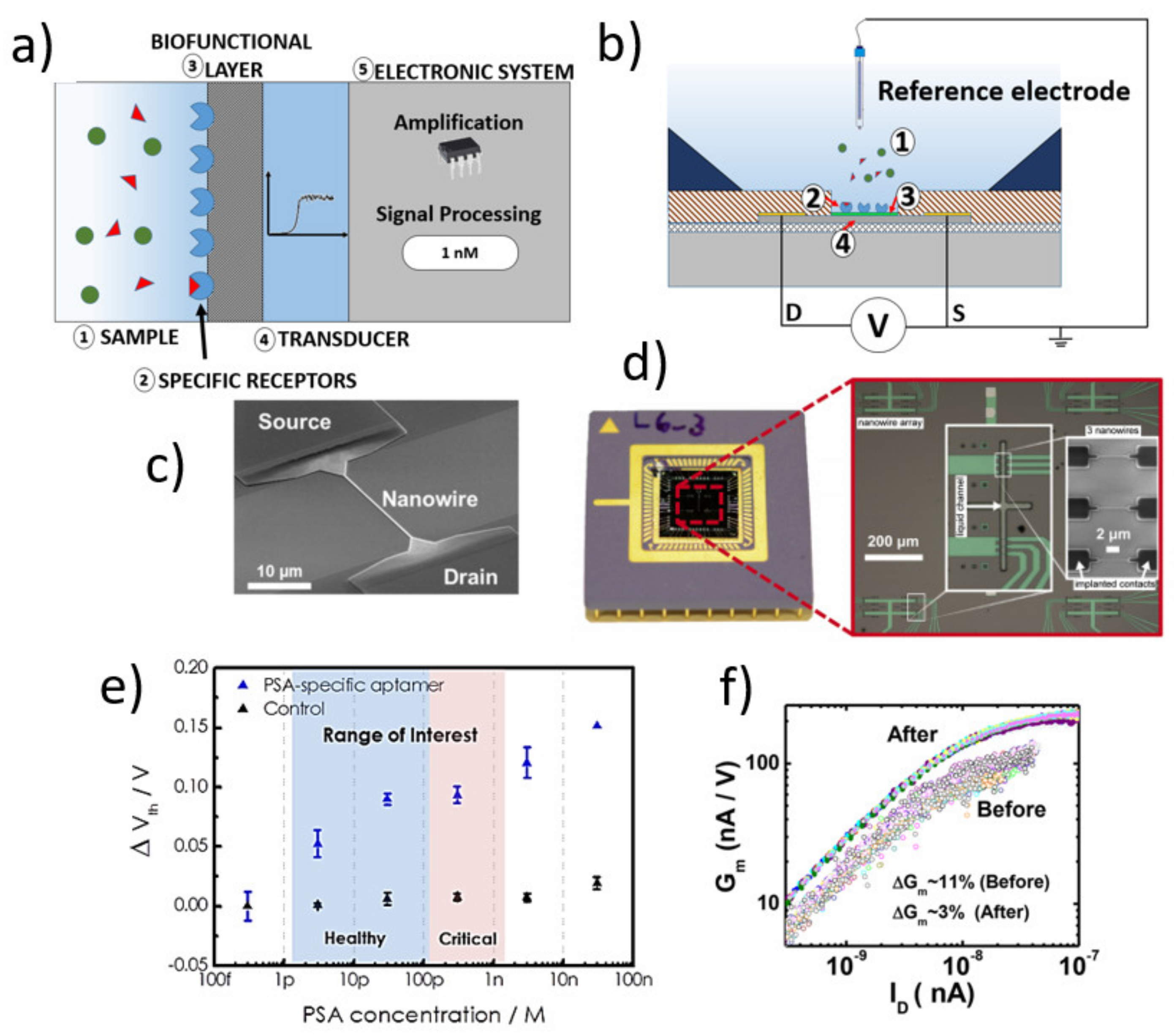
2. SiNW-FET Biosensor
2.1. Structure of SiNW FET-Based Biosensors
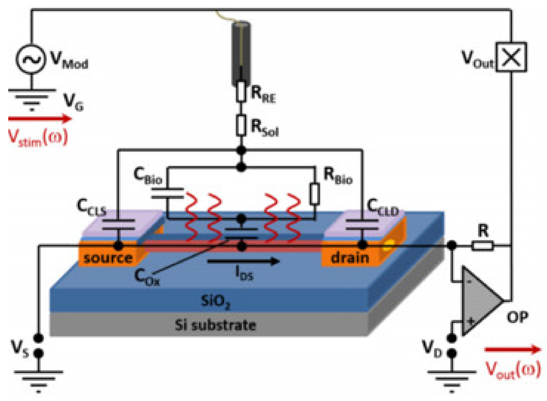
2.2. Readout Methods of SiNW-FETs
3. Design and Fabrication Considerations of SiNW-FET Biosensors
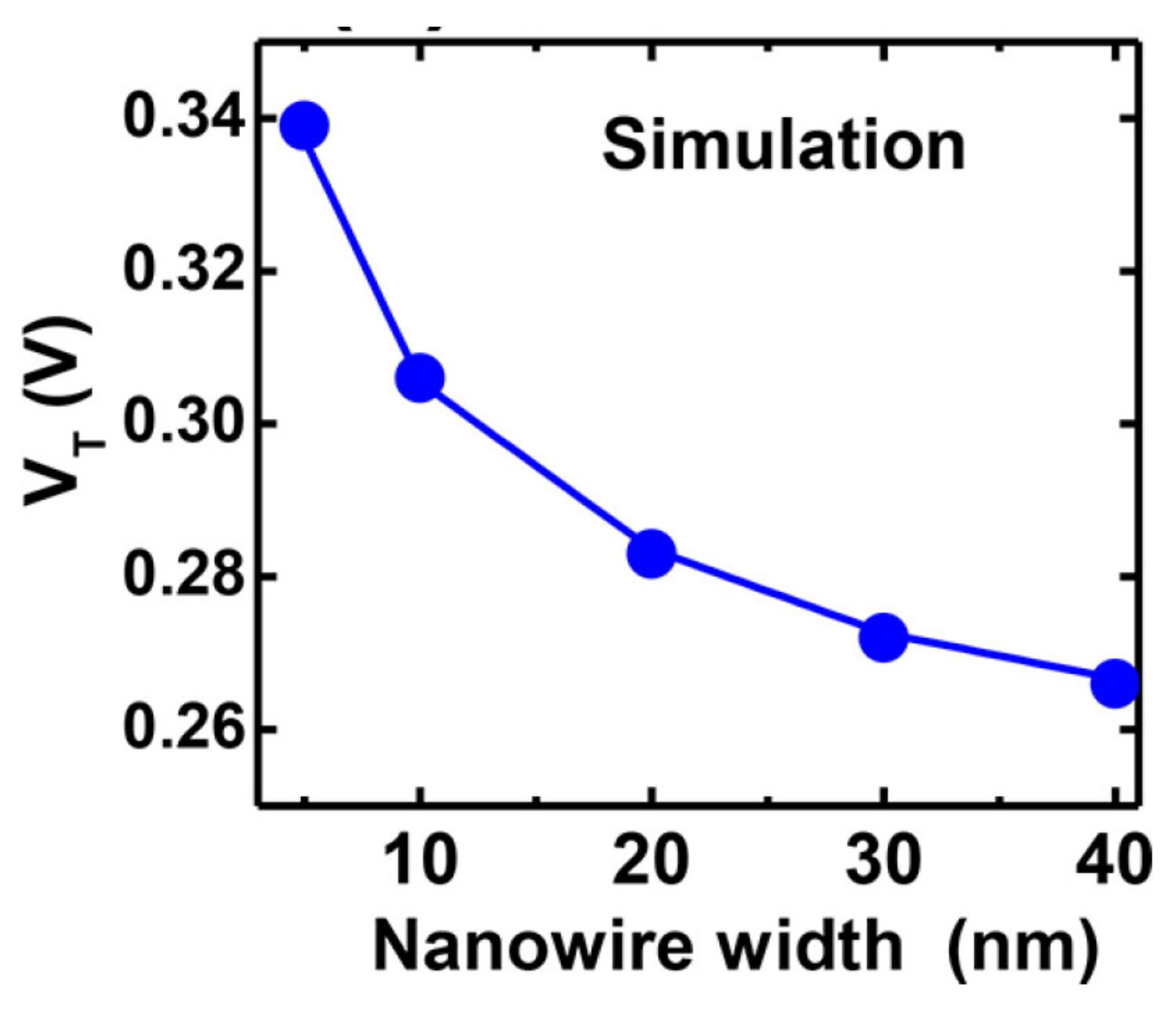
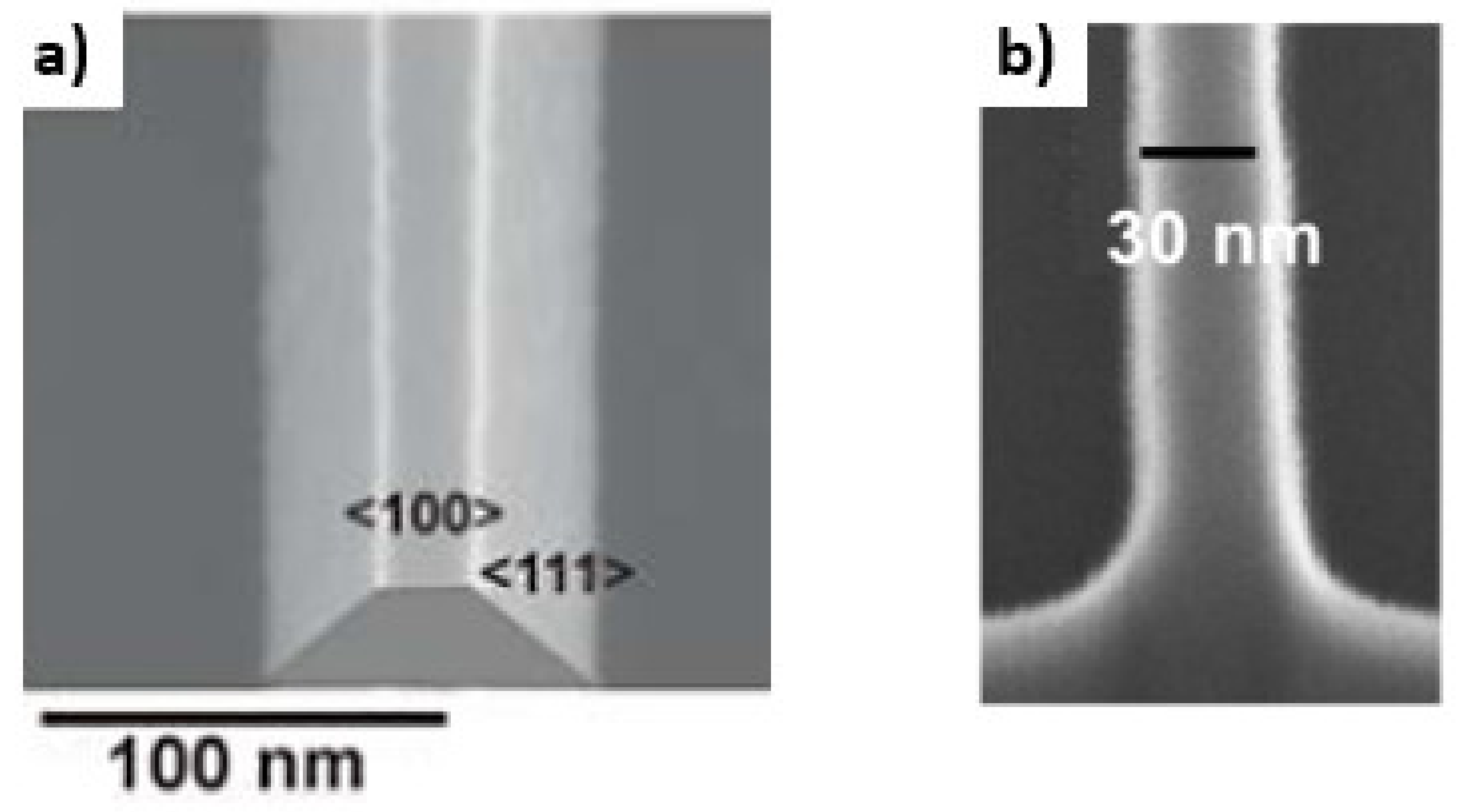
3.1. Nanowire: Dimensions and Pattering Method
3.2. The Drain and Source Contacts
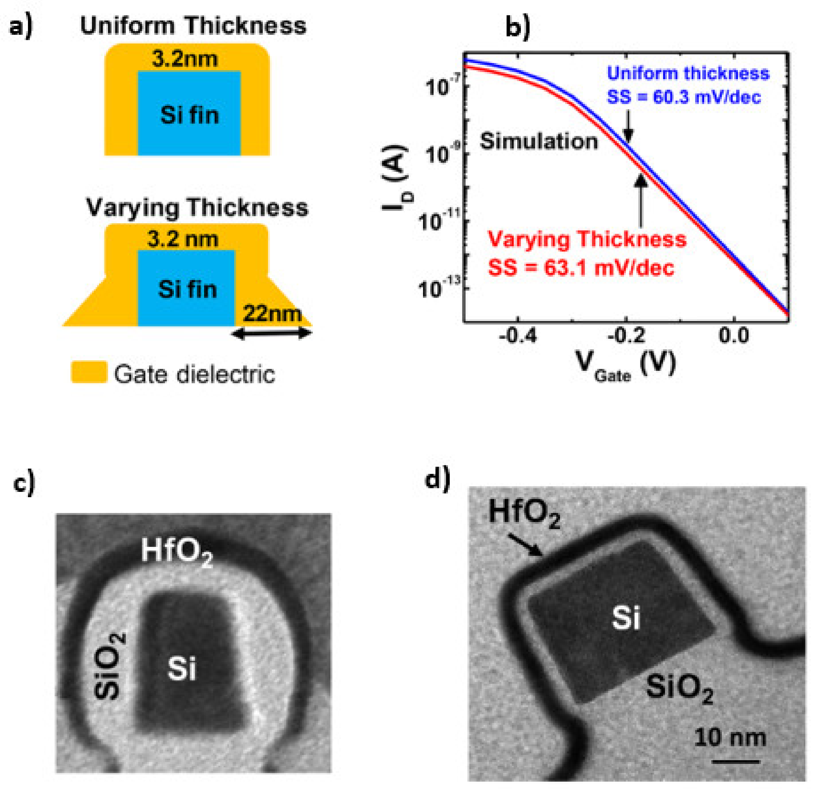
3.3. The Gate Oxide
4. Fabrication Methods for SiNW Based Biosensors
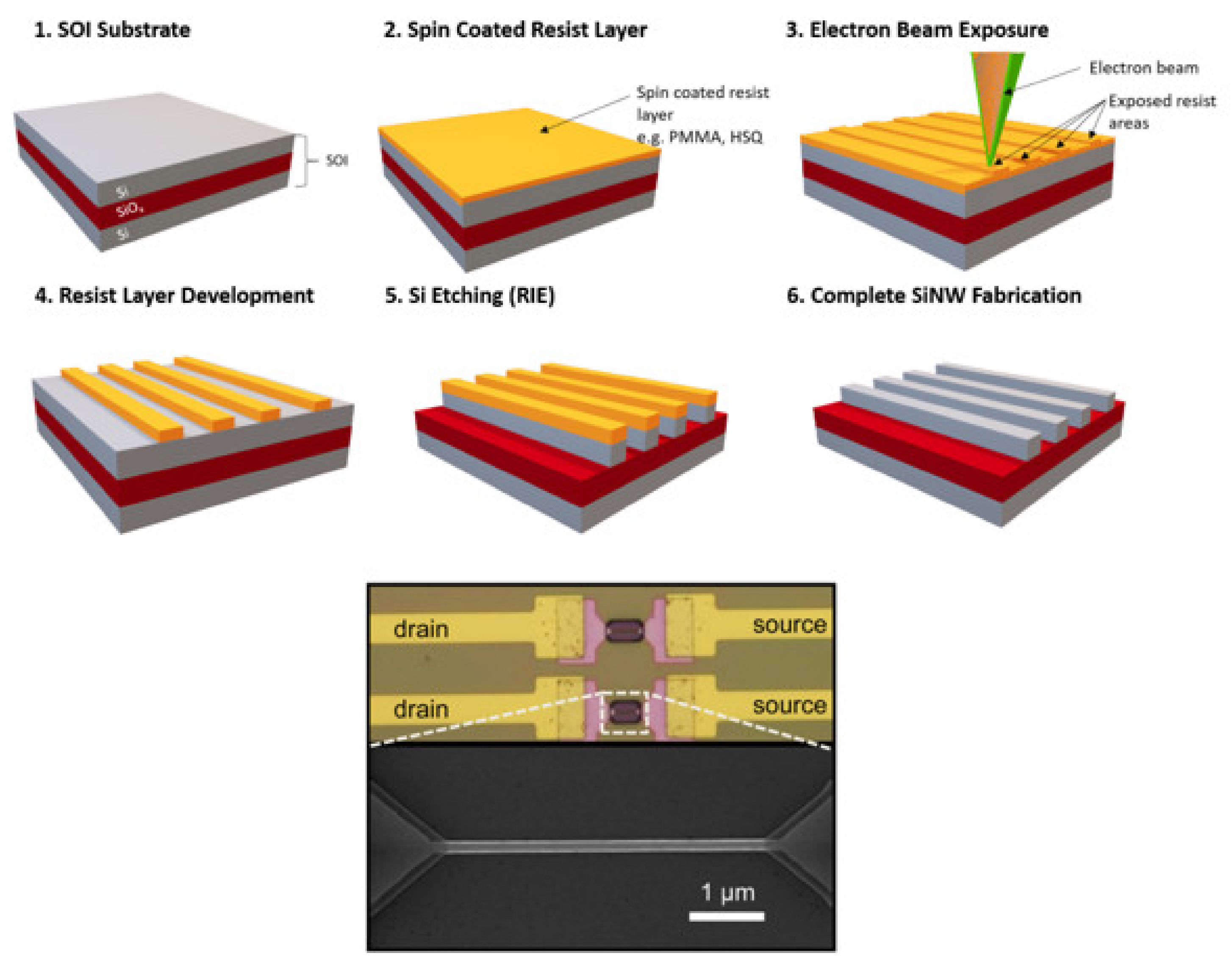
4.1. Electron Beam Lithography (EBL)
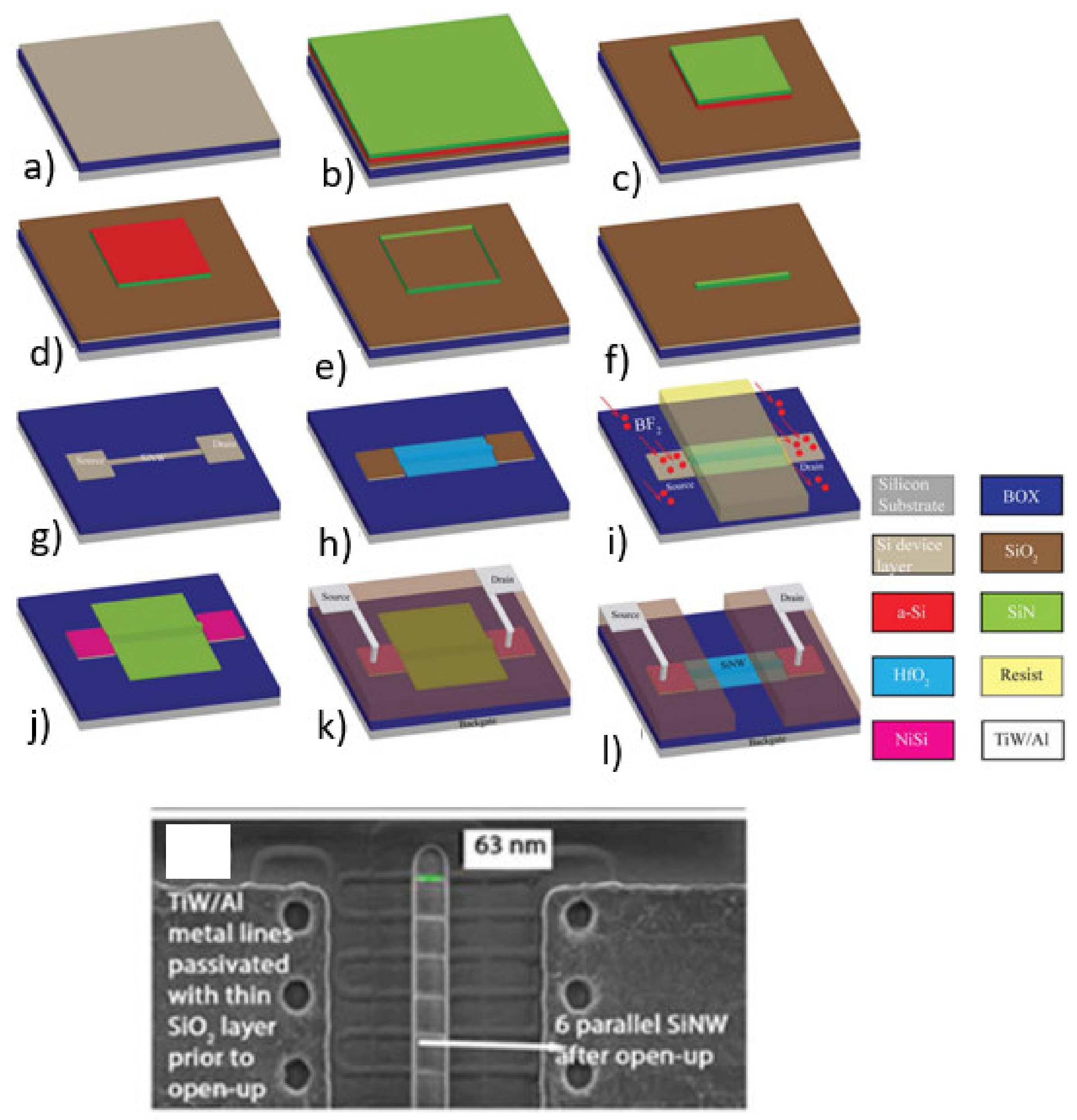
4.2. Sidewall Transfer Lithography (STL)
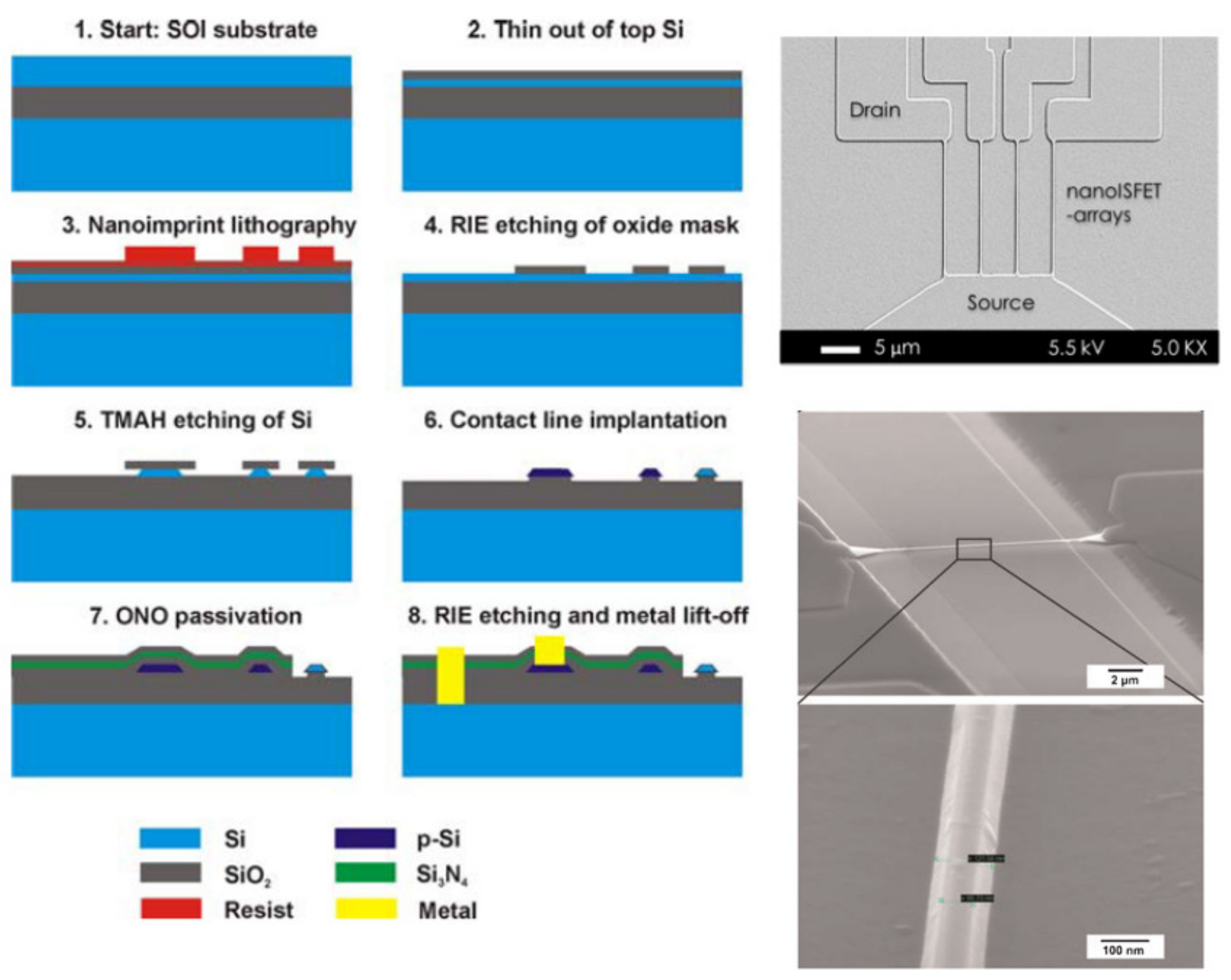
4.3. Nanoimprint Lithography (NIL)
5. System Integration
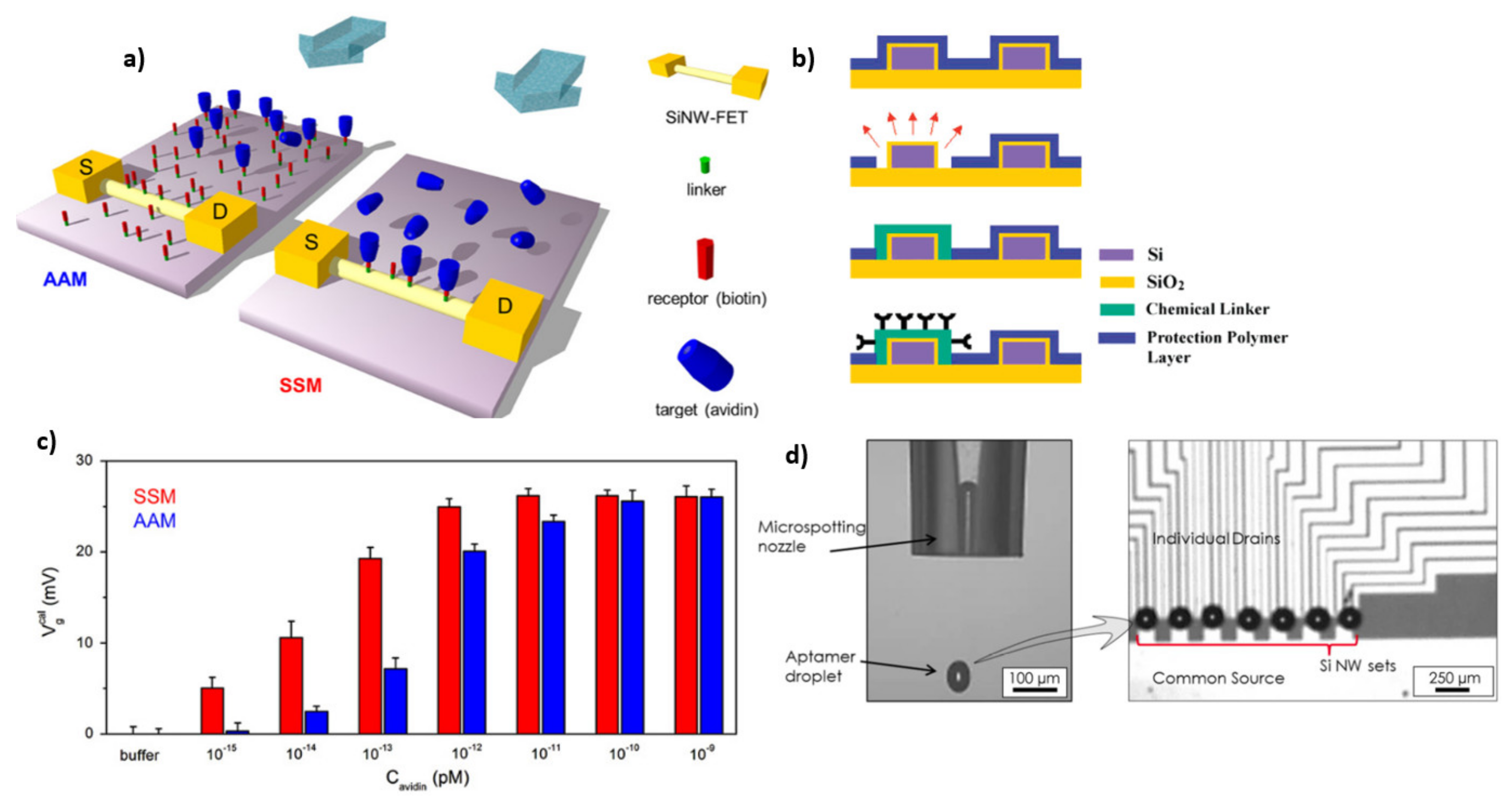
5.1. Surface Functionalization for Biosensing Applications
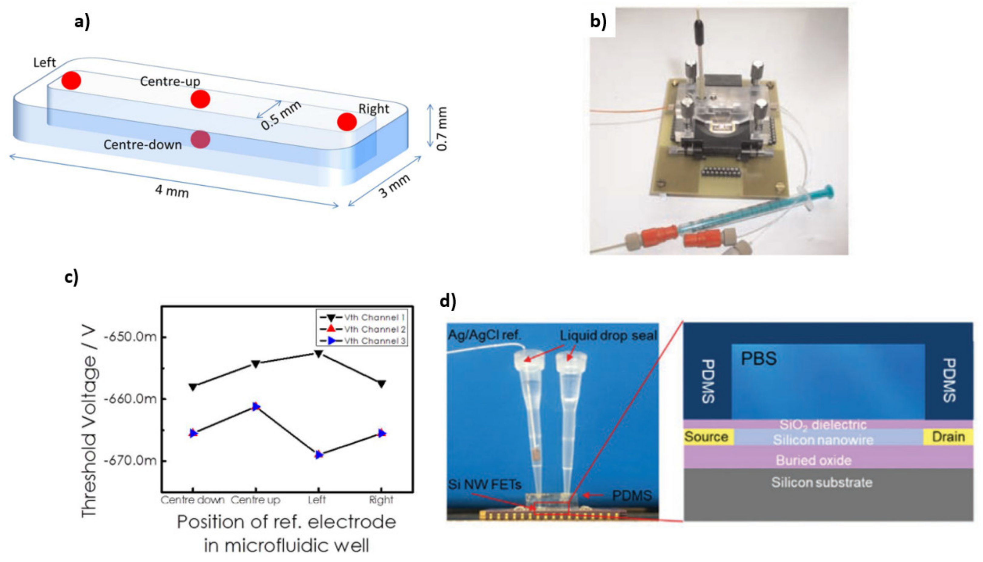
5.2. Microfluidic Integration
6. Conclusions and Outlook
Author Contributions
Funding
Institutional Review Board Statement
Informed Consent Statement
Acknowledgments
Conflicts of Interest
References
- Dincer, C.; Bruch, R.; Costa-Rama, E.; Fernandez-Abedul, M.T.; Merkoci, A.; Manz, A.; Urban, G.A.; Guder, F. Disposable Sensors in Diagnostics, Food, and Environmental Monitoring. Adv. Mater. 2019, 31, e1806739. [Google Scholar] [CrossRef]
- Li, J.; Kutovyi, Y.; Zadorozhnyi, I.; Boichuk, N.; Vitusevich, S. Monitoring of Dynamic Processes during Detection of Cardiac Biomarkers Using Silicon Nanowire Field-Effect Transistors. Adv. Mater. Interfaces 2020, 7, 2000508. [Google Scholar] [CrossRef]
- Vacic, A.; Criscione, J.M.; Stern, E.; Rajan, N.K.; Fahmy, T.; Reed, M.A. Multiplexed SOI BioFETs. Biosens Bioelectron 2011, 28, 239–242. [Google Scholar] [CrossRef] [PubMed]
- Zheng, G.; Patolsky, F.; Cui, Y.; Wang, W.U.; Lieber, C.M. Multiplexed electrical detection of cancer markers with nanowire sensor arrays. Nat. Biotechnol. 2005, 23, 1294–1301. [Google Scholar] [CrossRef]
- Cui, Y.; Wei, Q.; Park, H.; Lieber, C.M. Nanowire nanosensors for highly sensitive and selective detection of biological and chemical species. Science 2001, 293, 1289–1292. [Google Scholar] [CrossRef] [PubMed]
- Rani, D.; Pachauri, V.; Madaboosi, N.; Jolly, P.; Vu, X.T.; Estrela, P.; Chu, V.; Conde, J.P.; Ingebrandt, S. Top-Down Fabricated Silicon Nanowire Arrays for Field-Effect Detection of Prostate-Specific Antigen. ACS Omega 2018, 3, 8471–8482. [Google Scholar] [CrossRef]
- Gao, Z.; Agarwal, A.; Trigg, A.D.; Singh, N.; Fang, C.; Tung, C.-H.; Fan, Y.; Buddharaju, K.D.; Kong, J.J.A.C. Silicon nanowire arrays for label-free detection of DNA. Anal. Chem. 2007, 79, 3291–3297. [Google Scholar] [CrossRef]
- Schwartz, M.; Nguyen, T.C.; Vu, X.T.; Wagner, P.; Thoelen, R.; Ingebrandt, S. Impedimetric Sensing of DNA with Silicon Nanowire Transistors as Alternative Transducer Principle. Phys. Status Solidi 2018, 215, 1700740. [Google Scholar] [CrossRef]
- Eschermann, J.F.; Stockmann, R.; Hueske, M.; Vu, X.T.; Ingebrandt, S.; Offenhäusser, A. Action potentials of HL-1 cells recorded with silicon nanowire transistors. Appl. Phys. Lett. 2009, 95, 083703. [Google Scholar] [CrossRef]
- Delacour, C.; Veliev, F.; Crozes, T.; Bres, G.; Minet, J.; Ionica, I.; Ernst, T.; Briançon-Marjollet, A.; Albrieux, M.; Villard, C.J.A.E.M. Neuron-Gated Silicon Nanowire Field Effect Transistors to Follow Single Spike Propagation within Neuronal Network. Adv. Eng. Mater. 2021, 23, 2001226. [Google Scholar] [CrossRef]
- Patolsky, F.; Timko, B.P.; Yu, G.; Fang, Y.; Greytak, A.B.; Zheng, G.; Lieber, C.M.J.S. Detection, stimulation, and inhibition of neuronal signals with high-density nanowire transistor arrays. Science 2006, 313, 1100–1104. [Google Scholar] [CrossRef] [PubMed]
- Anand, A.; Liu, C.-R.; Chou, A.-C.; Hsu, W.-H.; Ulaganathan, R.K.; Lin, Y.-C.; Dai, C.-A.; Tseng, F.-G.; Pan, C.-Y.; Chen, Y.-T.J.A.S. Detection of K+ efflux from stimulated cortical neurons by an aptamer-modified silicon nanowire field-effect transistor. ACS Sens. 2017, 2, 69–79. [Google Scholar] [CrossRef]
- Zafar, S.; D’Emic, C.; Jagtiani, A.; Kratschmer, E.; Miao, X.; Zhu, Y.; Mo, R.; Sosa, N.; Hamann, H.; Shahidi, G. Silicon Nanowire Field Effect Transistor Sensors with Minimal Sensor-to-Sensor Variations and Enhanced Sensing Characteristics. ACS Nano 2018, 12, 6577–6587. [Google Scholar] [CrossRef]
- Li, H.; Dauphin-Ducharme, P.; Ortega, G.; Plaxco, K.W. Calibration-Free Electrochemical Biosensors Supporting Accurate Molecular Measurements Directly in Undiluted Whole Blood. J. Am. Chem. Soc. 2017, 139, 11207–11213. [Google Scholar] [CrossRef]
- Rani, D.; Pachauri, V.; Ingebrandt, S. Silicon Nanowire Field-Effect Biosensors. In Label-Free Biosensing; Springer: Berlin, Germany, 2018; pp. 27–57. [Google Scholar]
- Tran, D.P.; Pham, T.T.T.; Wolfrum, B.; Offenhausser, A.; Thierry, B. CMOS-Compatible Silicon Nanowire Field-Effect Transistor Biosensor: Technology Development toward Commercialization. Materials 2018, 11, 785. [Google Scholar] [CrossRef] [PubMed]
- Namdari, P.; Daraee, H.; Eatemadi, A. Recent Advances in Silicon Nanowire Biosensors: Synthesis Methods, Properties, and Applications. Nanoscale Res. Lett 2016, 11, 406. [Google Scholar] [CrossRef] [PubMed]
- Lee, S.; Wang, N.; Zhang, Y.; Tang, Y.J.M.B. Oxide-assisted semiconductor nanowire growth. Mrs Bull. 1999, 24, 36–42. [Google Scholar] [CrossRef]
- Patolsky, F.; Zheng, G.; Lieber, C.M. Fabrication of silicon nanowire devices for ultrasensitive, label-free, real-time detection of biological and chemical species. Nat. Protoc. 2006, 1, 1711–1724. [Google Scholar] [CrossRef] [PubMed]
- Kim, A.; Ah, C.S.; Yu, H.Y.; Yang, J.-H.; Baek, I.-B.; Ahn, C.-G.; Park, C.W.; Jun, M.S.; Lee, S.J.A.P.L. Ultrasensitive, label-free, and real-time immunodetection using silicon field-effect transistors. Appl. Phys. Lett. 2007, 91, 103901. [Google Scholar] [CrossRef]
- Gao, A.; Lu, N.; Dai, P.; Li, T.; Pei, H.; Gao, X.; Gong, Y.; Wang, Y.; Fan, C. Silicon-nanowire-based CMOS-compatible field-effect transistor nanosensors for ultrasensitive electrical detection of nucleic acids. Nano Lett. 2011, 11, 3974–3978. [Google Scholar] [CrossRef]
- Vu, X.T.; Eschermann, J.F.; Stockmann, R.; GhoshMoulick, R.; Offenhäusser, A.; Ingebrandt, S. Top-down processed silicon nanowire transistor arrays for biosensing. Phys. Status Solidi 2009, 206, 426–434. [Google Scholar] [CrossRef]
- Jayakumar, G.; Garidis, K.; Hellström, P.-E.; Östling, M. Fabrication and characterization of silicon nanowires using STL for biosensing applications. In Proceedings of the 15th International Conference on Ultimate Integration on Silicon (ULIS), Stockholm, Sweden, 7–9 April 2014; pp. 109–112. [Google Scholar]
- Park, I.; Li, Z.; Pisano, A.P.; Williams, R.S. Top-down fabricated silicon nanowire sensors for real-time chemical detection. Nanotechnology 2010, 21, 015501. [Google Scholar] [CrossRef]
- Vu, X.; GhoshMoulick, R.; Eschermann, J.; Stockmann, R.; Offenhäusser, A.; Ingebrandt, S. Fabrication and application of silicon nanowire transistor arrays for biomolecular detection. Sens. Actuators B Chem. 2010, 144, 354–360. [Google Scholar] [CrossRef]
- Müller, A.; Vu, X.T.; Pachauri, V.; Francis, L.A.; Flandre, D.; Ingebrandt, S. Wafer-Scale Nanoimprint Lithography Process Towards Complementary Silicon Nanowire Field-Effect Transistors for Biosensor Applications. Phys. Status Solidi 2018, 215, 1800234. [Google Scholar] [CrossRef]
- Rani, D.; Pachauri, V.; Mueller, A.; Vu, X.T.; Nguyen, T.C.; Ingebrandt, S. On the Use of Scalable NanoISFET Arrays of Silicon with Highly Reproducible Sensor Performance for Biosensor Applications. ACS Omega 2016, 1, 84–92. [Google Scholar] [CrossRef] [PubMed]
- Rani, D.; Singh, Y.; Salker, M.; Vu, X.T.; Ingebrandt, S.; Pachauri, V. Point-of-care-ready nanoscale ISFET arrays for sub-picomolar detection of cytokines in cell cultures. Anal. Bioanal. Chem. 2020, 1–12. [Google Scholar] [CrossRef]
- Vu, X.T.; Stockmann, R.; Wolfrum, B.; Offenhäusser, A.; Ingebrandt, S. Fabrication and application of a microfluidic-embedded silicon nanowire biosensor chip. Phys. Status Solidi 2010, 207, 850–857. [Google Scholar] [CrossRef]
- Stern, E.; Klemic, J.F.; Routenberg, D.A.; Wyrembak, P.N.; Turner-Evans, D.B.; Hamilton, A.D.; LaVan, D.A.; Fahmy, T.M.; Reed, M.A. Label-free immunodetection with CMOS-compatible semiconducting nanowires. Nature 2007, 445, 519–522. [Google Scholar] [CrossRef]
- Smith, R.; Geary, S.M.; Salem, A.K. Silicon Nanowires and Their Impact on Cancer Detection and Monitoring. ACS Appl. Nano Mater. 2020, 3, 8522–8536. [Google Scholar] [CrossRef]
- Doucey, M.-A.; Carrara, S. Nanowire sensors in cancer. Trends Biotechnol. 2019, 37, 86–99. [Google Scholar] [CrossRef] [PubMed]
- Pachauri, V.; Ingebrandt, S. Biologically sensitive field-effect transistors: From ISFETs to NanoFETs. Essays Biochem. 2016, 60, 81–90. [Google Scholar] [CrossRef]
- Tian, B.; Lieber, C.M. Nanowired Bioelectric Interfaces. Chem. Rev. 2019, 119, 9136–9152. [Google Scholar] [CrossRef] [PubMed]
- Kaisti, M. Detection principles of biological and chemical FET sensors. Biosens. Bioelectron. 2017, 98, 437–448. [Google Scholar] [CrossRef]
- Noor, M.O.; Krull, U.J. Silicon nanowires as field-effect transducers for biosensor development: A review. Anal. Chim. Acta 2014, 825, 1–25. [Google Scholar] [CrossRef]
- Zhang, G.J.; Ning, Y. Silicon nanowire biosensor and its applications in disease diagnostics: A review. Anal. Chim. Acta 2012, 749, 1–15. [Google Scholar] [CrossRef]
- Baraban, L.; Ibarlucea, B.; Baek, E.; Cuniberti, G. Hybrid Silicon Nanowire Devices and Their Functional Diversity. Adv. Sci. 2019, 6, 1900522. [Google Scholar] [CrossRef] [PubMed]
- Leonard, F.; Talin, A.A. Electrical contacts to one- and two-dimensional nanomaterials. Nat. Nanotechnol. 2011, 6, 773–783. [Google Scholar] [CrossRef] [PubMed]
- Livi, P.; Shadmani, A.; Wipf, M.; Stoop, R.L.; Rothe, J.; Chen, Y.; Calame, M.; Schönenberger, C.; Hierlemann, A. Sensor system including silicon nanowire ion sensitive FET arrays and CMOS readout. Sens. Actuators B Chem. 2014, 204, 568–577. [Google Scholar] [CrossRef]
- Tran, D.P.; Winter, M.; Yang, C.T.; Stockmann, R.; Offenhausser, A.; Thierry, B. Silicon Nanowires Field Effect Transistors: A Comparative Sensing Performance between Electrical Impedance and Potentiometric Measurement Paradigms. Anal. Chem. 2019, 91, 12568–12573. [Google Scholar] [CrossRef]
- Duan, X.; Li, Y.; Rajan, N.K.; Routenberg, D.A.; Modis, Y.; Reed, M.A. Quantification of the affinities and kinetics of protein interactions using silicon nanowire biosensors. Nat. Nanotechnol. 2012, 7, 401–407. [Google Scholar] [CrossRef]
- Bergveld, P. The operation of an ISFET as an electronic device. Sens. Actuators 1981, 1, 17–29. [Google Scholar] [CrossRef]
- Han, Y.; Offenhäusser, A.; Ingebrandt, S. Detection of DNA hybridization by a field-effect transistor with covalently attached catcher molecules. Surf. Interface Anal. 2006, 38, 176–181. [Google Scholar] [CrossRef]
- Gao, X.P.; Zheng, G.; Lieber, C.M. Subthreshold regime has the optimal sensitivity for nanowire FET biosensors. Nano Lett. 2010, 10, 547–552. [Google Scholar] [CrossRef] [PubMed]
- Nguyen, T.C.; Vu, X.T.; Freyler, M.; Ingebrandt, S. PSPICE model for silicon nanowire field-effect transistor biosensors in impedimetric measurement mode. Phys. Status Solidi 2013, 210, 870–876. [Google Scholar] [CrossRef]
- Bhattacharjee, A.; Nguyen, T.C.; Pachauri, V.; Ingebrandt, S.; Vu, X.T.J.M. Comprehensive Understanding of Silicon-Nanowire Field-Effect Transistor Impedimetric Readout for Biomolecular Sensing. Micromachines 2021, 12, 39. [Google Scholar] [CrossRef]
- Nair, P.R.; Alam, M.A. Design Considerations of Silicon Nanowire Biosensors. IEEE Trans. Electron. Devices 2007, 54, 3400–3408. [Google Scholar] [CrossRef]
- Park, C.W.; Ahn, C.G.; Yang, J.H.; Baek, I.B.; Ah, C.S.; Kim, A.; Kim, T.Y.; Sung, G.Y. Control of channel doping concentration for enhancing the sensitivity of ‘top-down’ fabricated Si nanochannel FET biosensors. Nanotechnology 2009, 20, 475501. [Google Scholar] [CrossRef]
- Bae, T.-E.; Jang, H.-J.; Yang, J.-H.; Cho, W.-J. High Performance of Silicon Nanowire-Based Biosensors using a High-k Stacked Sensing Thin Film. ACS Appl. Mater. Interfaces 2013, 5, 5214–5218. [Google Scholar] [CrossRef]
- Choi, S.; Park, I.; Hao, Z.; Holman, H.-Y.N.; Pisano, A.P. Quantitative studies of long-term stable, top-down fabricated silicon nanowire pH sensors. Appl. Phys. A 2012, 107, 421–428. [Google Scholar] [CrossRef]
- Tang, X.; Reckinger, N.; Larrieu, G.; Dubois, E.; Flandre, D.; Raskin, J.P.; Nysten, B.; Jonas, A.M.; Bayot, V. Characterization of ultrathin SOI film and application to short channel MOSFETs. Nanotechnology 2008, 19, 165703. [Google Scholar] [CrossRef][Green Version]
- Saha, S.K. Modeling process variability in scaled CMOS technology. IEEE Des. Test. Comput. 2010, 27, 8–16. [Google Scholar] [CrossRef]
- Regonda, S.; Tian, R.; Gao, J.; Greene, S.; Ding, J.; Hu, W. Silicon multi-nanochannel FETs to improve device uniformity/stability and femtomolar detection of insulin in serum. Biosens. Bioelectron. 2013, 45, 245–251. [Google Scholar] [CrossRef] [PubMed]
- Rajan, N.K.; Routenberg, D.A.; Jin, C.; Reed, M.A. 1/f Noise of Silicon Nanowire BioFETs. IEEE Electron. Device Lett. 2010, 31, 615–617. [Google Scholar] [CrossRef]
- Moh, T.S.Y.; Pandraud, G.; Sarro, P.M.; Huang, Q.A.; Sudhölter, E.J.R.; Nie, M.; de Smet, L.C.P.M. Effect of silicon nanowire etching on signal-to-noise ratio of SiNW FETs for (bio)sensor applications. Electron. Lett. 2013, 49, 782–784. [Google Scholar] [CrossRef]
- Schnakenberg, U.; Benecke, W.; Lange, P. TMAHW etchants for silicon micromachining. In Proceedings of the TRANSDUCERS’91: International Conference on Solid-State Sensors and Actuators, Digest of Technical Papers, San Francisco, CA, USA, 24–27 June 1991; pp. 815–818. [Google Scholar]
- Cui, Y.; Zhong, Z.; Wang, D.; Wang, W.U.; Lieber, C.M. High Performance Silicon Nanowire Field Effect Transistors. Nano Lett. 2003, 3, 149–152. [Google Scholar] [CrossRef]
- Kutovyi, Y.; Zadorozhnyi, I.; Hlukhova, H.; Handziuk, V.; Petrychuk, M.; Ivanchuk, A.; Vitusevich, S.J.N. Origin of noise in liquid-gated Si nanowire troponin biosensors. Nanotechnology 2018, 29, 175202. [Google Scholar] [CrossRef]
- Susloparova, A.; Vu, X.T.; Koppenhöfer, D.; Law, J.K.-Y.; Ingebrandt, S. Investigation of ISFET device parameters to optimize for impedimetric sensing of cellular adhesion. Phys. Status Solidi 2014, 211, 1395–1403. [Google Scholar] [CrossRef]
- Motayed, A.; Bonevich, J.E.; Krylyuk, S.; Davydov, A.V.; Aluri, G.; Rao, M.V. Correlation between the performance and microstructure of Ti/Al/Ti/Au Ohmic contacts to p-type silicon nanowires. Nanotechnology 2011, 22, 075206. [Google Scholar] [CrossRef]
- Lin, Y.C.; Chen, Y.; Xu, D.; Huang, Y. Growth of nickel silicides in Si and Si/SiOx core/shell nanowires. Nano Lett. 2010, 10, 4721–4726. [Google Scholar] [CrossRef]
- Sze, S.M. Semiconductor Devices: Physics and Technology; John Wiley & Sons: Hoboken, NJ, USA, 2008. [Google Scholar]
- Zhou, W.; Dai, X.; Fu, T.M.; Xie, C.; Liu, J.; Lieber, C.M. Long term stability of nanowire nanoelectronics in physiological environments. Nano Lett. 2014, 14, 1614–1619. [Google Scholar] [CrossRef]
- Kim, S.; Kwon, D.W.; Lee, R.; Kim, D.H.; Park, B.-G. Investigation of drift effect on silicon nanowire field effect transistor based pH sensor. Jpn. J. Appl. Phys. 2016, 55. [Google Scholar] [CrossRef]
- Rigante, S.; Scarbolo, P.; Wipf, M.; Stoop, R.L.; Bedner, K.; Buitrago, E.; Bazigos, A.; Bouvet, D.; Calame, M.; Schonenberger, C.; et al. Sensing with Advanced Computing Technology: Fin Field-Effect Transistors with High-k Gate Stack on Bulk Silicon. ACS Nano 2015, 9, 4872–4881. [Google Scholar] [CrossRef]
- Robertson, J. Interfaces and defects of high-K oxides on silicon. Solid State Electron. 2005, 49, 283–293. [Google Scholar] [CrossRef]
- Zafar, S.; Callegari, A.; Gusev, E.; Fischetti, M.V. Charge trapping related threshold voltage instabilities in high permittivity gate dielectric stacks. J. Appl. Phys. 2003, 93, 9298–9303. [Google Scholar] [CrossRef]
- Zafar, S.; Kumar, A.; Gusev, E.; Cartier, E. Threshold voltage instabilities in high-/spl kappa/ gate dielectric stacks. IEEE Trans. Device Mater. Reliab. 2005, 5, 45–64. [Google Scholar] [CrossRef]
- Guillorn, M.; Chang, J.; Fuller, N.; Patel, J.; Darnon, M.; Pyzyna, A.; Joseph, E.; Engelmann, S.; Ott, J.; Newbury, J.; et al. Hydrogen silsesquioxane-based hybrid electron beam and optical lithography for high density circuit prototyping. J. Vac. Sci. Technol. B 2009, 27, 2588–2592. [Google Scholar] [CrossRef]
- Drennan, P.G.; McAndrew, C.C. Understanding MOSFET mismatch for analog design. IEEE J. Solid-State Circuits 2003, 38, 450–456. [Google Scholar] [CrossRef]
- Rajan, N.K.; Routenberg, D.A.; Reed, M.A. Optimal signal-to-noise ratio for silicon nanowire biochemical sensors. Appl. Phys. Lett. 2011, 98, 264107–2641073. [Google Scholar] [CrossRef]
- Lee, J.; Jang, J.; Choi, B.; Yoon, J.; Kim, J.Y.; Choi, Y.K.; Kim, D.M.; Kim, D.H.; Choi, S.J. A Highly Responsive Silicon Nanowire/Amplifier MOSFET Hybrid Biosensor. Sci. Rep. 2015, 5, 12286. [Google Scholar] [CrossRef]
- Jayakumar, G.; Legallais, M.; Hellstrom, P.E.; Mouis, M.; Pignot-Paintrand, I.; Stambouli, V.; Ternon, C.; Ostling, M. Wafer-scale HfO2 encapsulated silicon nanowire field effect transistor for efficient label-free DNA hybridization detection in dry environment. Nanotechnology 2019, 30, 184002. [Google Scholar] [CrossRef]
- Lim, C.M.; Lee, I.K.; Lee, K.J.; Oh, Y.K.; Shin, Y.B.; Cho, W.J. Improved sensing characteristics of dual-gate transistor sensor using silicon nanowire arrays defined by nanoimprint lithography. Sci. Technol. Adv. Mater. 2017, 18, 17–25. [Google Scholar] [CrossRef]
- Yu, Z.; Chen, L.; Wu, W.; Ge, H.; Chou, S.Y. Fabrication of nanoscale gratings with reduced line edge roughness using nanoimprint lithography. J. Vac. Sci. Technol. B 2003, 21. [Google Scholar] [CrossRef][Green Version]
- Sreenivasan, S.V. Nanoimprint lithography steppers for volume fabrication of leading-edge semiconductor integrated circuits. Microsyst. Nanoeng. 2017, 3, 17075. [Google Scholar] [CrossRef] [PubMed]
- Li, B.R.; Chen, C.W.; Yang, W.L.; Lin, T.Y.; Pan, C.Y.; Chen, Y.T. Biomolecular recognition with a sensitivity-enhanced nanowire transistor biosensor. Biosens. Bioelectron. 2013, 45, 252–259. [Google Scholar] [CrossRef] [PubMed]
- Han, Y.; Mayer, D.; Offenhäusser, A.; Ingebrandt, S. Surface activation of thin silicon oxides by wet cleaning and silanization. Thin Solid Film. 2006, 510, 175–180. [Google Scholar] [CrossRef]
- Munief, W.M.; Heib, F.; Hempel, F.; Lu, X.L.; Schwartz, M.; Pachauri, V.; Hempelmann, R.; Schmitt, M.; Ingebrandt, S. Silane Deposition via Gas-Phase Evaporation and High-Resolution Surface Characterization of the Ultrathin Siloxane Coatings. Langmuir 2018, 34, 10217–10229. [Google Scholar] [CrossRef]
- Uslu, F.; Ingebrandt, S.; Mayer, D.; Bocker-Meffert, S.; Odenthal, M.; Offenhausser, A. Labelfree fully electronic nucleic acid detection system based on a field-effect transistor device. Biosens. Bioelectron. 2004, 19, 1723–1731. [Google Scholar] [CrossRef] [PubMed]
- Park, I.; Li, Z.; Pisano, A.P.; Williams, R.S. Selective surface functionalization of silicon nanowires via nanoscale Joule heating. Nano Lett. 2007, 7, 3106–3111. [Google Scholar] [CrossRef]
- Rani, D. Label-free Detection of Biomolecules Using Silicon Nanowire Ion-sensitive Field-effect Transistor Devices. Ph.D. Thesis, Justus-Liebig-Universität Gießen, Giessen, Germany, 2017. [Google Scholar]
- Reimhult, E.; Höök, F.J.S. Design of surface modifications for nanoscale sensor applications. Sensors 2015, 15, 1635–1675. [Google Scholar] [CrossRef] [PubMed]
- Kalia, J.; Raines, R.T.J. Advances in bioconjugation. Curr. Org. Chem. 2010, 14, 138–147. [Google Scholar] [CrossRef]
- Knopp, D.; Tang, D.; Niessner, R.J.A. Bioanalytical applications of biomolecule-functionalized nanometer-sized doped silica particles. Anal. Chim. Acta 2009, 647, 14–30. [Google Scholar] [CrossRef]
- Camarero, J.A.J. Recent developments in the site-specific immobilization of proteins onto solid supports. Pept. Sci. 2008, 90, 450–458. [Google Scholar] [CrossRef]
- Tzouvadaki, I.; Zapatero-Rodríguez, J.; Naus, S.; de Micheli, G.; O’Kennedy, R.; Carrara, S.J.S.; Chemical, A.B. Memristive biosensors based on full-size antibodies and antibody fragments. Sens. Actuators B 2019, 286, 346–352. [Google Scholar] [CrossRef]
- Ingebrandt, S.J.N. Sensing beyond the Limit. Nat. Nanotechnol. 2015, 10, 734–735. [Google Scholar] [CrossRef]
- Lu, B.; Smyth, M.R.; O’Kennedy, R.J.A. Tutorial review. Oriented immobilization of antibodies and its applications in immunoassays and immunosensors. Analyst 1996, 121, 29R–32R. [Google Scholar] [CrossRef]
- Linshiz, G.; Jensen, E.; Stawski, N.; Bi, C.; Elsbree, N.; Jiao, H.; Kim, J.; Mathies, R.; Keasling, J.D.; Hillson, N.J. End-to-end automated microfluidic platform for synthetic biology: From design to functional analysis. J. Biol. Eng. 2016, 10, 1–15. [Google Scholar] [CrossRef] [PubMed]
- Huang, I.Y.; Huang, R.S. Fabrication and characterization of a new planar solid-state reference electrode for ISFET sensors. Thin Solid Film. 2002, 406, 255–261. [Google Scholar] [CrossRef]
- Shinwari, M.W.; Zhitomirsky, D.; Deen, I.A.; Selvaganapathy, P.R.; Deen, M.J.; Landheer, D. Microfabricated Reference Electrodes and their Biosensing Applications. Sensors 2010, 10, 1679–1715. [Google Scholar] [CrossRef] [PubMed]
- Yang, H.; Kang, S.K.; Choi, C.A.; Kim, H.; Shin, D.-H.; Kim, Y.S.; Kim, Y.T. An iridium oxide reference electrode for use in microfabricated biosensors and biochips. Lab Chip 2004, 4, 42–46. [Google Scholar] [CrossRef] [PubMed]
- Lewenstam, A. Handbook of Reference Electrodes; György, I., Andrzej, L., Fritz, S., Eds.; Springer: Berlin, Germany, 2013; pp. 1–344. ISBN 978-3-642-36187-6. [Google Scholar]
- Duarte-Guevara, C.; Swaminathan, V.V.; Burgess, M.; Reddy, B.; Salm, E.; Liu, Y.S.; Rodriguez-Lopez, J.; Bashir, R. On-chip metal/polypyrrole quasi-reference electrodes for robust ISFET operation. Analyst 2015, 140, 3630–3641. [Google Scholar] [CrossRef] [PubMed]
- Kremers, T.; Tintelott, M.; Pachauri, V.; Vu, X.T.; Ingebrandt, S.; Schnakenberg, U. Microelectrode Combinations of Gold and Polypyrrole Enable Highly Stable Two-Electrode Electrochemical Impedance Spectroscopy Measurements Under Turbulent Flow Conditions. Electroanalysis 2020, 33, 197–207. [Google Scholar] [CrossRef]


| Etching Process | Hooge Constant αH | Subthreshold Swing | Reference |
|---|---|---|---|
| TMAH | 0.0021 | 1.0 V/decade | [55] |
| Cl2 (ICP) | 0.015 | 2.6 V/decade | [55] |
| CF4 (RIE) | 0.017 | 3.0 V/decade | [55] |
| Approach | Doping Process Parameters | Doping Concentration | Metal | References |
|---|---|---|---|---|
| Ion implantation and silicide formation | (B) 2.5 keV, 4 × 10¹⁵ ions/cm2 | ~8 × 10¹⁹ atoms/cm−3 | NiPt (10% Pt)/TiN | [13] |
| Ion implantation and Al contacts | (B) 7 keV, 1 × 10¹⁴ ions/cm2 | N/A | Al/Ti/Au | [22] |
| Ion implantation and Ti/Al contacts | (BF2+) 8 keV, 5 × 10¹⁵ ions/cm2 | N/A | Ti/Al | [3] |
| Gate Material | pH Sensitivity (mV/pH) | Drift Rate (mV/h) | Hysteresis (mV) |
|---|---|---|---|
| SiO2 | 38.7 | 45.24 | 173 |
| SiO2/Si3N4 | 49.7 | 3.86 | 20.9 |
| SiO2/HfO2 | 55.3 | 1.88 | 6.9 |
| SiO2/Ta2O5 | 52.6 | 0.61 | 13.9 |
| SiO2/ZrO2 | 53.9 | 0.44 | 22.1 |
| SiO2/Al2O3 | 53.1 | 0.25 | 0.6 |
| Fabrication Approach | NW Size in Width and Length | Vth and Its Variation | CMOS Integration | References |
|---|---|---|---|---|
| Top-down fabrication on SOI wafer, EBL process using HSQ combined with optical lithography | 30 nm, 5 µm | 0.28 ± 0.028 V | No | [13] |
| Top-down fabrication on SOI wafer, EBL process using HSQ combined with optical lithography | 50 nm, 20 µm | 1.15 ± 0.16 V | No | [54] |
| Top-down fabrication on SOI wafer, EBL process using HSQ combined with optical lithography | 55 nm, N/A | N/A | Yes | [73] |
| Top-down fabrication on SOI wafer, optical lithography | Nanoribbon | −2.3 ± 0.15 V | No | [3] |
| Fabrication Approach | NW Size in Width and Length | Vth and Its Variation | CMOS Integration | References |
|---|---|---|---|---|
| Top-down fabrication on SOI wafer, NIL | 125 nm × 15 µm | 0.384 ± 0.106 V | No | [27] |
| Top-down fabrication on SOI wafer, NIL | 100 nm × 7 µm | 0.65 ± 0.3 V | No | [26] |
Publisher’s Note: MDPI stays neutral with regard to jurisdictional claims in published maps and institutional affiliations. |
© 2021 by the authors. Licensee MDPI, Basel, Switzerland. This article is an open access article distributed under the terms and conditions of the Creative Commons Attribution (CC BY) license (https://creativecommons.org/licenses/by/4.0/).
Share and Cite
Tintelott, M.; Pachauri, V.; Ingebrandt, S.; Vu, X.T. Process Variability in Top-Down Fabrication of Silicon Nanowire-Based Biosensor Arrays. Sensors 2021, 21, 5153. https://doi.org/10.3390/s21155153
Tintelott M, Pachauri V, Ingebrandt S, Vu XT. Process Variability in Top-Down Fabrication of Silicon Nanowire-Based Biosensor Arrays. Sensors. 2021; 21(15):5153. https://doi.org/10.3390/s21155153
Chicago/Turabian StyleTintelott, Marcel, Vivek Pachauri, Sven Ingebrandt, and Xuan Thang Vu. 2021. "Process Variability in Top-Down Fabrication of Silicon Nanowire-Based Biosensor Arrays" Sensors 21, no. 15: 5153. https://doi.org/10.3390/s21155153
APA StyleTintelott, M., Pachauri, V., Ingebrandt, S., & Vu, X. T. (2021). Process Variability in Top-Down Fabrication of Silicon Nanowire-Based Biosensor Arrays. Sensors, 21(15), 5153. https://doi.org/10.3390/s21155153