Temperature Gradient Method for Alleviating Bonding-Induced Warpage in a High-Precision Capacitive MEMS Accelerometer


 , , and
Abstract
1. Introduction
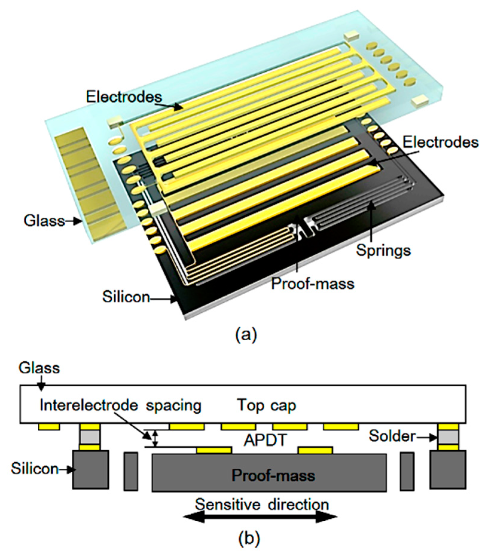
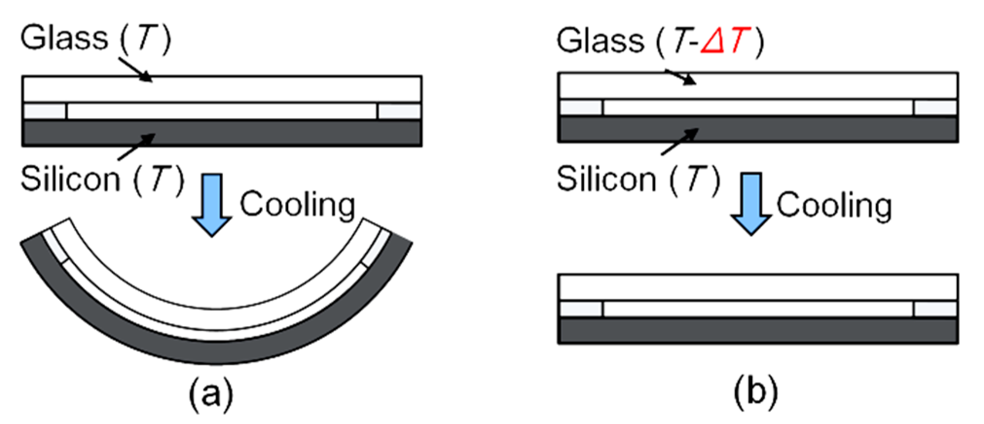
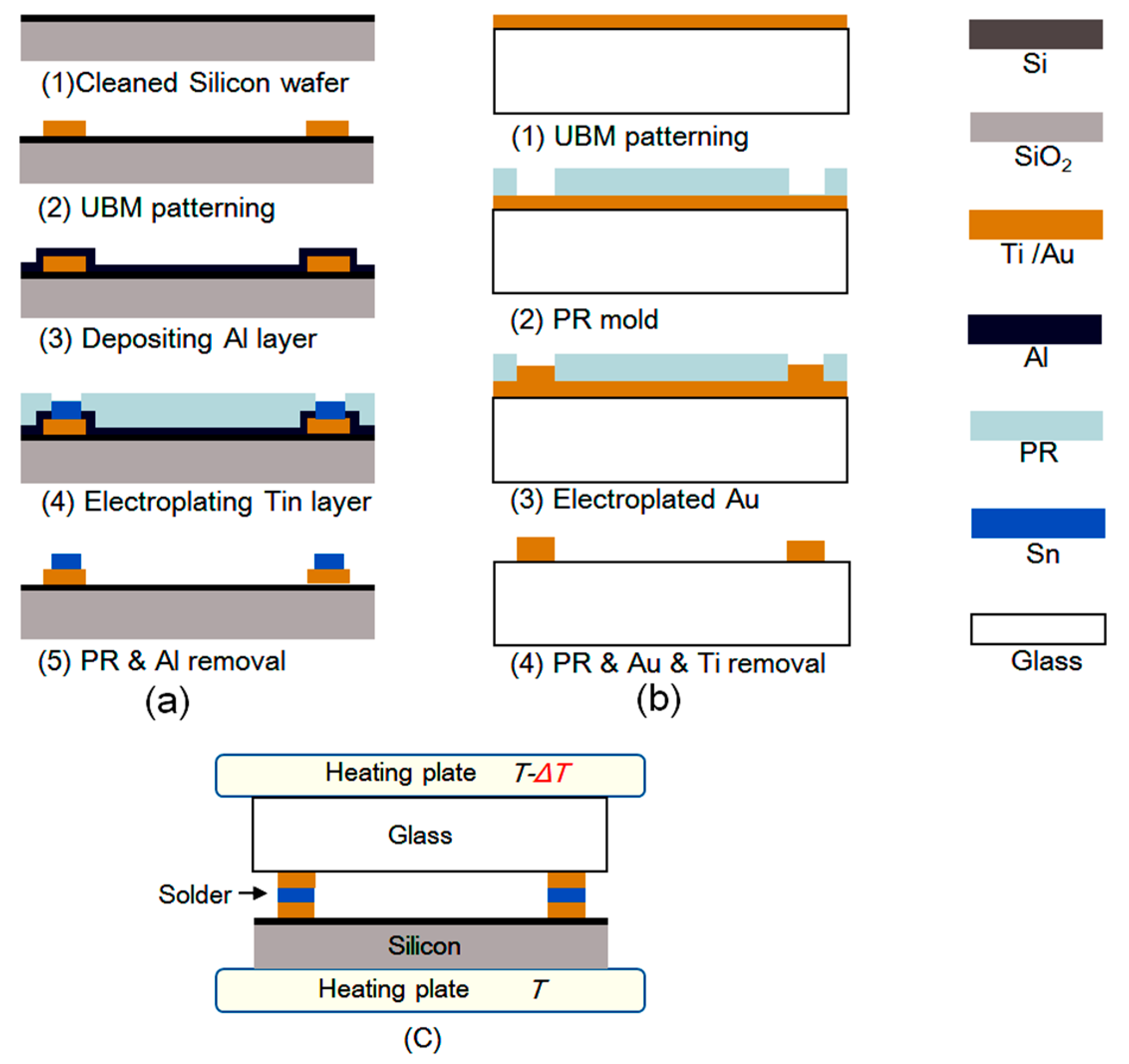
2. Design
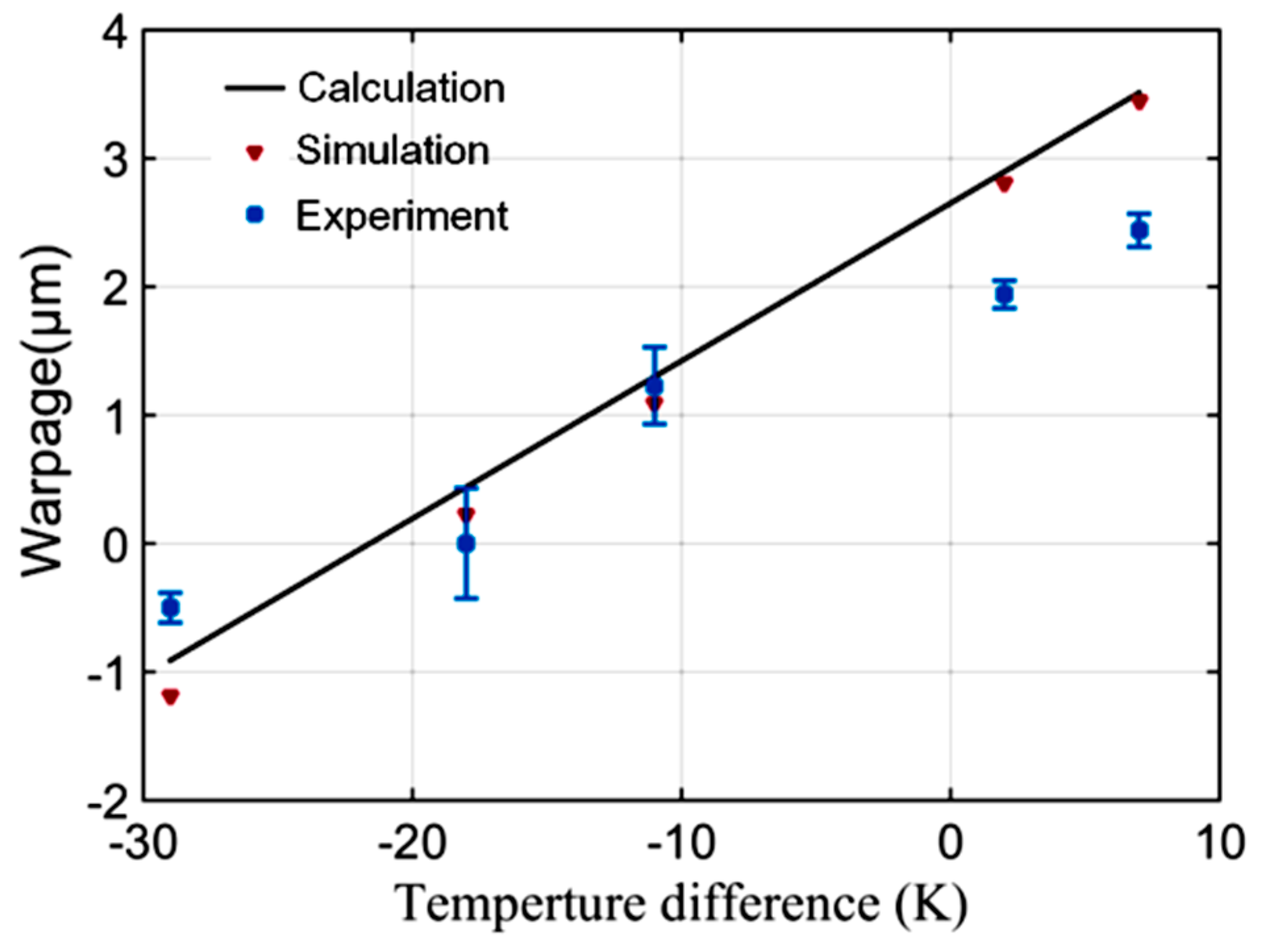
3. Experiment and Simulation
4. Results
5. Conclusions
Author Contributions
Funding
Acknowledgments
Conflicts of Interest
Appendix A


| E (GPa) | v | CTE (ppmK-1) | Thermal Conductivity (W/m.K) | Thickness (μm) | Width (mm) | Length (mm) | |
|---|---|---|---|---|---|---|---|
| Spring-mass | Equation (A5) | 0.28 | Equation (A6) | 13.1 | 500 | 20 | 20 |
| Top cap | 72.4 | 0.25 | 3.25 | 1.2 | 500 | 20 | 20 |
| Eq-solder | 6.53 | 0.04 | 2.62 | 11.9 | 22.0 | 20 | 20 |
References
- Middlemiss, R.P.; Samarelli, A.; Paul, D.J.; Hough, J.; Rowan, S.; Hammond, G.D. Measurement of the Earth tides with a MEMS gravimeter. Nature 2016, 531, 614–617. [Google Scholar] [CrossRef] [PubMed]
- Wu, W.J.; Li, Z.; Liu, J.Q.; Fan, J.; Tu, L.C. A nano-g MEMS accelerometer for earthquake monitoring. In Proceedings of the 19th International Conference on Solid-State Sensors, Actuators and Microsystems (TRANSDUCERS), Kaohsiung, Taiwan, 18–22 June 2017; pp. 599–602. [Google Scholar]
- Milligan, D.J.; Homeijer, B.D.; Walmsley, R.G. An ultra-low noise MEMS accelerometer for seismic imaging. Proc. IEEE Sens. 2011, 1281–1284. [Google Scholar] [CrossRef]
- Zwahlen, P.; Dong, Y.; Nguyen, A.-M.; Rudolf, F.; Stauffer, J.-M.; Ullah, P.; Ragot, V. Breakthrough in high performance inertial navigation grade Sigma-Delta MEMS accelerometer. In Proceedings of the 2012 IEEE/ION Position, Location and Navigation Symposium, Myrtle Beach, SC, USA, 23–26 April 2012; pp. 15–19. [Google Scholar]
- Pike, W.T.; Kumar, S. Improved design of micromachined lateral suspensions using intermediate frames. J. Micromech. Microeng. 2007, 17, 1680–1694. [Google Scholar] [CrossRef]
- Walmsley, R.G.; Kiyama, L.K.; Milligan, D.M.; Alley, R.L.; Erickson, D.L.; Hartwell, P.G. Micro-G silicon accelerometer using surface electrodes. In Proceedings of the 2009 IEEE Sensors, Christchurch, New Zealand, 25–28 October 2009; pp. 971–974. [Google Scholar]
- Benmessaoud, M.; Nasreddine, M.M. Optimization of MEMS capacitive accelerometer. Microsyst. Technol. 2013, 19, 713–720. [Google Scholar] [CrossRef]
- Keshavarzi, M.; YavandHasani, J. Design and optimization of fully differential capacitive MEMS accelerometer based on surface micromachining. Microsyst. Technol. 2019, 25, 1369–1377. [Google Scholar] [CrossRef]
- Tez, S.; Torunbalci, M.M.; Akin, T. A novel method for fabricating MEMS three-axis accelerometers using low temperature Au-Sn eutectic bonding. In Proceedings of the 2016 IEEE SENSORS, Orlando, FL, USA, 30 October–3 November 2016; pp. 1–3. [Google Scholar]
- Wu, W.J.; Zheng, P.P.; Liu, J.Q.; Li, Z.; Fan, J.; Liu, H.F.; Tu, L.C. High-Sensitivity Encoder-Like Micro Area-Changed Capacitive Transducer for a Nano-g Micro Accelerometer. Sensors 2017, 17, 2158. [Google Scholar] [CrossRef]
- Wu, W.J.; Liu, D.D.; Qiu, W.R.; Liu, H.F.; Hu, F.J.; Fan, J.; Hu, C.Y.; Tu, L.C. A precise spacing-control method in MEMS packaging for capacitive accelerometer applications. J. Micromech. Microeng. 2018, 28, 125016. [Google Scholar] [CrossRef]
- Jayaram, V.; McCann, S.; Huang, T.-C.; Kawamoto, S.; Pulugurtha, R.; Smet, V.; Tummala, R. Thermocompression Bonding Process Design and Optimization for Warpage Mitigation of Ultra-Thin Low-CTE Package Assemblies. In Proceedings of the 2016 IEEE 66th Electronic Components and Technology Conference (ECTC), Las Vegas, NV, USA, 31 May–3 June 2016; pp. 101–107. [Google Scholar]
- Yao, W.; Belhenini, S.; Roqueta, F.; Pujos, C.; Bruno, E.; Gardes, P.; Tougui, A. Intrinsic stress effects on the warpage of silicon substrate during thin film deposition, photolithography and etching processes. In Proceedings of the 2016 17th International Conference on Thermal, Mechanical and Multi-Physics Simulation and Experiments in Microelectronics and Microsystems (EuroSimE), Montpellier, France, 18–20 April 2016; pp. 1–6. [Google Scholar]
- Wang, P.J.; Kim, J.S.; Lee, C.C. A new bonding technology dealing with large CTE mismatch between large Si chips and Cu substrates. In Proceedings of the 2008 58th Electronic Components and Technology Conference, Lake Buena Vista, FL, USA, 27–30 May 2008; pp. 1562–1568. [Google Scholar]
- Hsieh, H.S.; Chang, H.C.; Hu, C.F.; Cheng, C.L.; Fang, W. A novel stress isolation guard-ring design for the improvement of a three-axis piezoresistive accelerometer. J. Micromech. Microeng. 2011, 21, 1412–1415. [Google Scholar] [CrossRef]
- Hao, Y.; Yuan, W.; Xie, J.; Shen, Q.; Chang, H. Design and Verification of a Structure for Isolating Packaging Stress in SOI MEMS Devices. IEEE Sens. J. 2017, 17, 1246–1254. [Google Scholar] [CrossRef]
- Zhang, Z.; Wu, J.; Bernard, S.; Walmsley, R.G. Chip on Board development for a novel MEMS accelerometer for seismic imaging. In Proceedings of the 2012 IEEE 62nd Electronic Components and Technology Conference, San Diego, CA, USA, 29 May–1 June 2012; pp. 350–355. [Google Scholar]
- Rogers, T. Considerations of anodic bonding for capacitive type silicon/glass sensor fabrication. J. Micromech. Microeng. 1992, 2, 164–166. [Google Scholar] [CrossRef]
- Rogers, T.; Kowal, J. Selection of glass, anodic bonding conditions and material compatibility for silicon-glass capacitive sensors. Sens. Actuators A 1995, 46, 113–120. [Google Scholar] [CrossRef]
- Matko, V.; Milanovic, M. Temperature-compensated capacitance-frequency converter with high resolution. Sens. Actuators A Phys. 2014, 220, 262–269. [Google Scholar] [CrossRef]
- Ivanov, V. Direct electro-optic effect in langasites and α-quartz. Opt. Mater. 2018, 79, 1–7. [Google Scholar] [CrossRef]
- Matko, V.; Šafarič, R. Major improvements of quartz crystal pulling sensitivity and linearity using series reactance. Sensors 2009, 9, 8263–8270. [Google Scholar] [CrossRef]
- Pike, W.T.; Delahunty, A.K.; Mukherjee, A.; Dou, G.; Liu, H.; Calcutt, S.; Standley, I.M. A self-levelling nano-g silicon seismometer. In Proceedings of the IEEE SENSORS 2014 Proceedings, Valencia, Spain, 2–5 November 2014; pp. 1599–1602. [Google Scholar]
- Wei, X.L.; Liu, J.Q.; Liu, H.F.; Wu, W.J.; Fan, J.; Tu, L.C. Electroplating of 3D Sn-rich solder for MEMS packaging applications. J. Micromech. Microeng. 2019, 29, 045008. [Google Scholar] [CrossRef]
- Tada, H.; Kumpel, A.E.; Lathrop, R.E.; Slanina, J.B.; Nieva, P.; Zavracky, P.; Miaoulis, I.N.; Wong, P.Y. Thermal expansion coefficient of polycrystalline silicon and silicon dioxide thin films at high temperatures. J. Appl. Phys. 2000, 87, 4189–4193. [Google Scholar] [CrossRef]
- Jan, M.T.; Ahmad, F.; Hamid, N.H.B.; MdKhir, M.H.B.; Ashraf, K.; Shoaib, M. Temperature dependent Young’s modulus and quality factor of CMOS-MEMS resonator: Modelling and experimental approach. Microelectron. Reliab. 2016, 57, 64–70. [Google Scholar] [CrossRef]
- Wang, H.J.; Deng, H.A.; Chiang, S.Y.; Su, Y.F.; Chiang, K.N. Development of a process modeling for residual stress assessment of multilayer thin film structure. Thin Solid Films 2015, 584, 146–153. [Google Scholar] [CrossRef]
- Freund, L.B.; Floro, J.A.; Chason, E. Extensions of the Stoney formula for substrate curvature to configurations with thin substrates or large deformations. Appl. Phys. Lett. 1999, 74, 1987–1989. [Google Scholar] [CrossRef]
- Yao, W.Z.; Roqueta, F.; Craveur, J.C.; Belhenini, S.; Gardes, P.; Tougui, A. Modelling and analysis of the stress distribution in a multi-thin film system Pt/USG/Si. Mater. Res. Express 2018, 5, 046405. [Google Scholar] [CrossRef]
- Hsueh, C.-H. Modeling of elastic deformation of multilayers due to residual stresses and external bending. J. Appl. Phys. 2002, 91, 9652–9656. [Google Scholar] [CrossRef]
- Torun, H.; Urey, H. Thermal deflections in multilayer microstructures and athermalization. J. Appl. Phys. 2006, 100, 023527. [Google Scholar] [CrossRef]
- Hu, Y.Y.; Huang, W.M. Elastic and elastic-plastic analysis of multilayer thin films: Closed-form solutions. J. Appl. Phys. 2004, 96, 4154–4160. [Google Scholar] [CrossRef]
- Okada, Y.; Tokumaru, Y. Precise determination of lattice parameter and thermal expansion coefficient of silicon between 300 and 1500 K. J. Appl. Phys. 1984, 56, 314–320. [Google Scholar] [CrossRef]


| No. | 1 | 2 | 3 | 4 | 5 |
|---|---|---|---|---|---|
| Si | 504 K | 504 K | 504 K | 504 K | 504 K |
| Glass | 475 K | 486 K | 493 K | 506 K | 511 K |
| ΔT (TSi–Tglass) | −29 K | −18 K | −11 K | +2 K | +7 K |
| Accelerometers | University of Glasgow [1] | Imperial College [23] | Hewlett Packard [3] | This Work |
|---|---|---|---|---|
| Applications | Gravimeter | Seismic Sensor | Seismic Sensor | Acceleration Sensor |
| Self-noise (ng/√Hz) | 10 | 2 | 10 | 6 |
© 2020 by the authors. Licensee MDPI, Basel, Switzerland. This article is an open access article distributed under the terms and conditions of the Creative Commons Attribution (CC BY) license (http://creativecommons.org/licenses/by/4.0/).
Share and Cite
Liu, D.; Liu, H.; Liu, J.; Hu, F.; Fan, J.; Wu, W.; Tu, L. Temperature Gradient Method for Alleviating Bonding-Induced Warpage in a High-Precision Capacitive MEMS Accelerometer. Sensors 2020, 20, 1186. https://doi.org/10.3390/s20041186
Liu D, Liu H, Liu J, Hu F, Fan J, Wu W, Tu L. Temperature Gradient Method for Alleviating Bonding-Induced Warpage in a High-Precision Capacitive MEMS Accelerometer. Sensors. 2020; 20(4):1186. https://doi.org/10.3390/s20041186
Chicago/Turabian StyleLiu, Dandan, Huafeng Liu, Jinquan Liu, Fangjing Hu, Ji Fan, Wenjie Wu, and Liangcheng Tu. 2020. "Temperature Gradient Method for Alleviating Bonding-Induced Warpage in a High-Precision Capacitive MEMS Accelerometer" Sensors 20, no. 4: 1186. https://doi.org/10.3390/s20041186
APA StyleLiu, D., Liu, H., Liu, J., Hu, F., Fan, J., Wu, W., & Tu, L. (2020). Temperature Gradient Method for Alleviating Bonding-Induced Warpage in a High-Precision Capacitive MEMS Accelerometer. Sensors, 20(4), 1186. https://doi.org/10.3390/s20041186