Author Contributions
Conceptualization, K.M. and C.S.; Data curation, K.M. and A.S.; Formal analysis, K.M. and A.S.; Funding acquisition, T.O. and H.K.; Investigation, K.M., M.M. and A.S.; Methodology, K.M., C.S., A.S. and R.F.; Project administration, C.S., R.F., S.Z. and K.H.; Supervision, C.S.; Writing—original draft, K.M., M.M. and A.S.; Writing—review & editing, C.S., R.F., S.Z. and K.H. All authors have read and agreed to the published version of the manuscript.
Figure 1.
Schematic of the presented aluminum nitride (AlN) micromirror designs.
Figure 1.
Schematic of the presented aluminum nitride (AlN) micromirror designs.
Figure 2.
The design procedure.
Figure 2.
The design procedure.
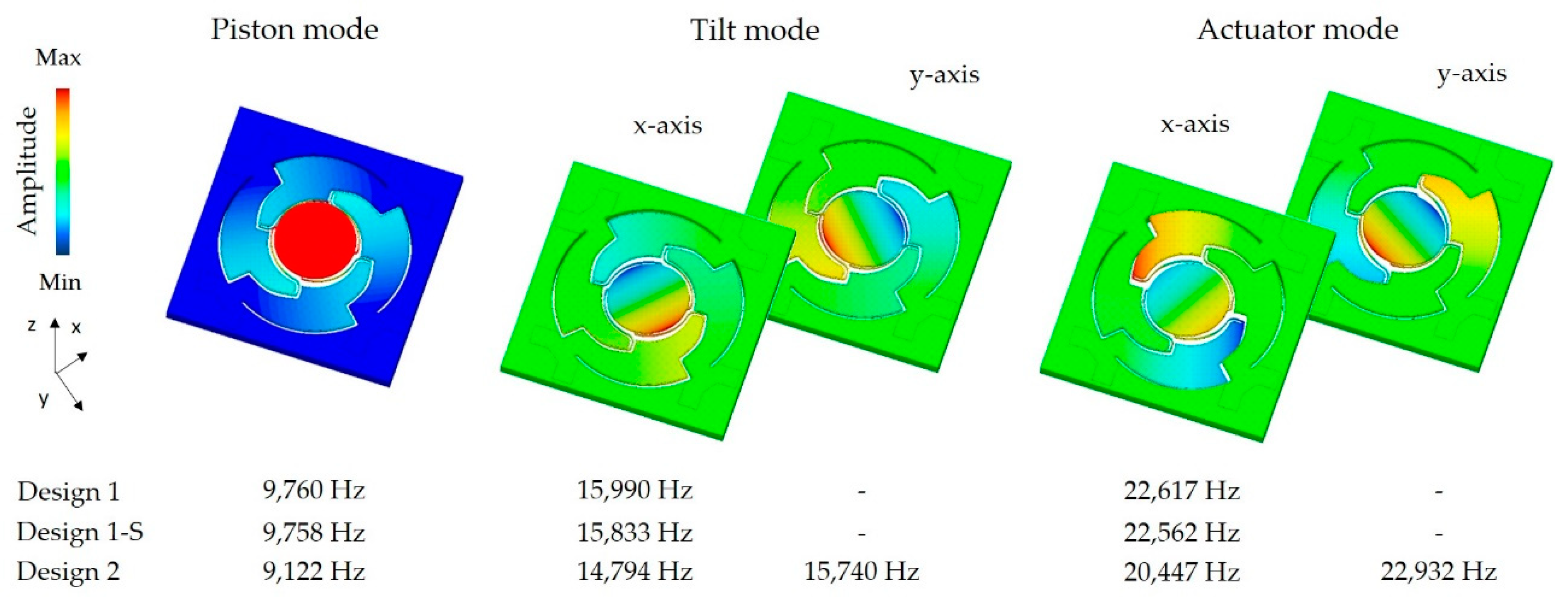
Figure 3.
Resulting out-of-plane modes up to 25,000 Hz for both micromirror designs simulated with ANSYS FEM with regard to the parameters summarized in
Table 2.
Figure 3.
Resulting out-of-plane modes up to 25,000 Hz for both micromirror designs simulated with ANSYS FEM with regard to the parameters summarized in
Table 2.
Figure 4.
Simulated influence of the device silicon thickness on the eigenfrequency (Design 1): (a) eigenfrequency deviation (deviation with respect to the eigenfrequency at 20 µm) versus device silicon thickness; (b) eigenfrequency versus device silicon thickness.
Figure 4.
Simulated influence of the device silicon thickness on the eigenfrequency (Design 1): (a) eigenfrequency deviation (deviation with respect to the eigenfrequency at 20 µm) versus device silicon thickness; (b) eigenfrequency versus device silicon thickness.
Figure 5.
Simulated influence of intrinsic prestress on the actuator offset-deflection: (a) tensile stress at wafer center; (b) compressive stress at wafer edge.
Figure 5.
Simulated influence of intrinsic prestress on the actuator offset-deflection: (a) tensile stress at wafer center; (b) compressive stress at wafer edge.
Figure 6.
Comparison of the simulated influences on the eigenfrequency of the tilt mode (Design 1): (a) eigenfrequency and eigenfrequency deviation (deviation with respect to the eigenfrequency at 18.5 µm) versus device silicon thickness; (b) eigenfrequency and eigenfrequency deviation (deviation with respect to the zero stress level) versus the effective mechanical stress.
Figure 7.
The fabrication process flow: (a) AlN deposition; (b) AlN wet etching; (c) Al deposition and structuring; (d) Backside Si etching by deep reactive ion etching (DRIE); (e) Device Si structuring.
Figure 7.
The fabrication process flow: (a) AlN deposition; (b) AlN wet etching; (c) Al deposition and structuring; (d) Backside Si etching by deep reactive ion etching (DRIE); (e) Device Si structuring.
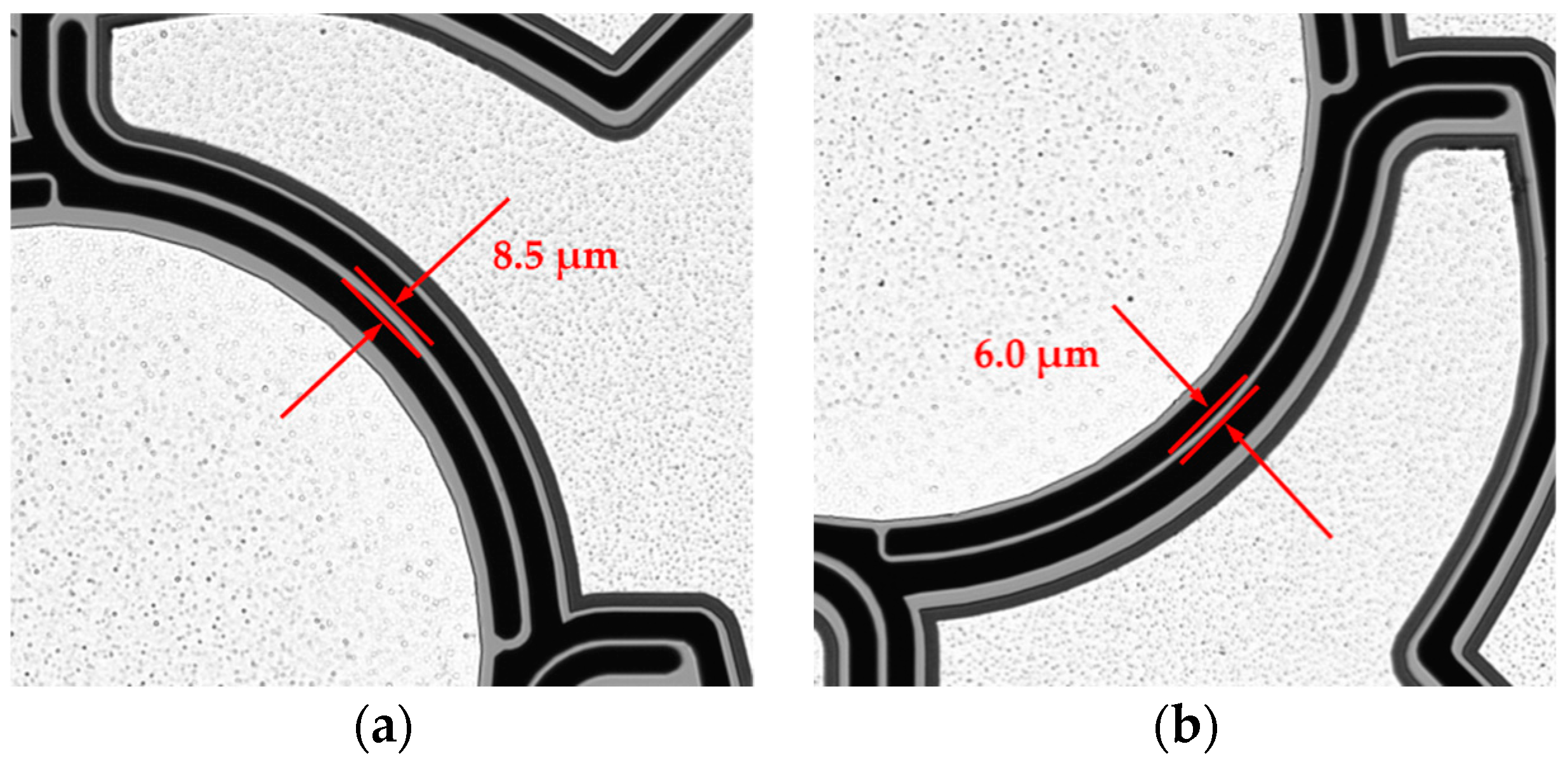
Figure 8.
Microscope image of the spring structures of a fabricated micromirror of Design 2. Technological deviations led to smaller resulting spring widths: (a) The 10 µm springs have a resulting width of 8.5 µm (b) The 7.5 µm springs have a resulting width of 6.0 µm.
Figure 8.
Microscope image of the spring structures of a fabricated micromirror of Design 2. Technological deviations led to smaller resulting spring widths: (a) The 10 µm springs have a resulting width of 8.5 µm (b) The 7.5 µm springs have a resulting width of 6.0 µm.
Figure 9.
Photography of the processed micromirror devices on wafer level captured by a stereo microscope: (a) Design 2; (b) Design 1-S.
Figure 9.
Photography of the processed micromirror devices on wafer level captured by a stereo microscope: (a) Design 2; (b) Design 1-S.
Figure 10.
Diced micromirrors of Design 2 (left) and Design 1-S (right) in size comparison to a ladybug (Coccinella septempunctata).
Figure 10.
Diced micromirrors of Design 2 (left) and Design 1-S (right) in size comparison to a ladybug (Coccinella septempunctata).
Figure 11.
Schematic of the optical test setup. The laser beam and screen were aligned in a defined distance at a 45 ° angle to the mirror. The illustrated scan angle, optical angle, and mechanical tilt angle could be calculated with (2) and (3).
Figure 11.
Schematic of the optical test setup. The laser beam and screen were aligned in a defined distance at a 45 ° angle to the mirror. The illustrated scan angle, optical angle, and mechanical tilt angle could be calculated with (2) and (3).
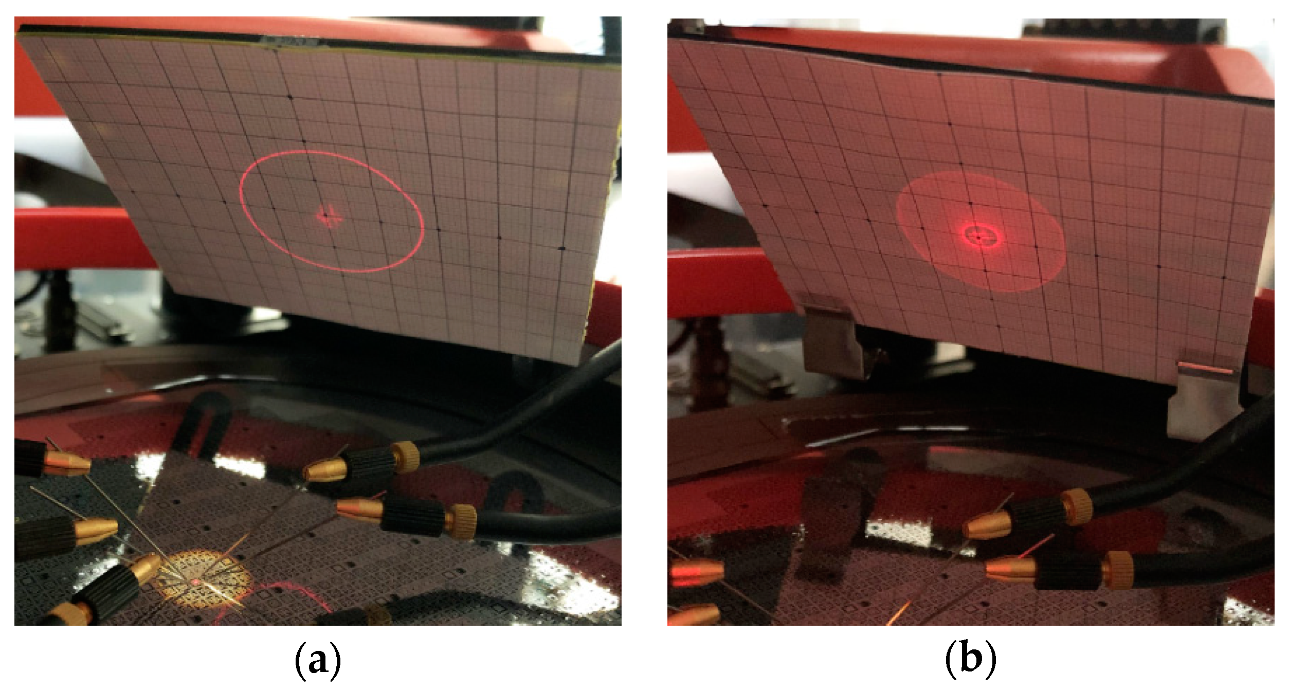
Figure 12.
Photograph of the optical test setup: (a) Entire setup around the automated probe bench station; (b) Integrated probe bench adapter with laser source holder and scaled screen.
Figure 12.
Photograph of the optical test setup: (a) Entire setup around the automated probe bench station; (b) Integrated probe bench adapter with laser source holder and scaled screen.
Figure 13.
Schematic of the sensor signal evaluation setup [
10].
Figure 13.
Schematic of the sensor signal evaluation setup [
10].
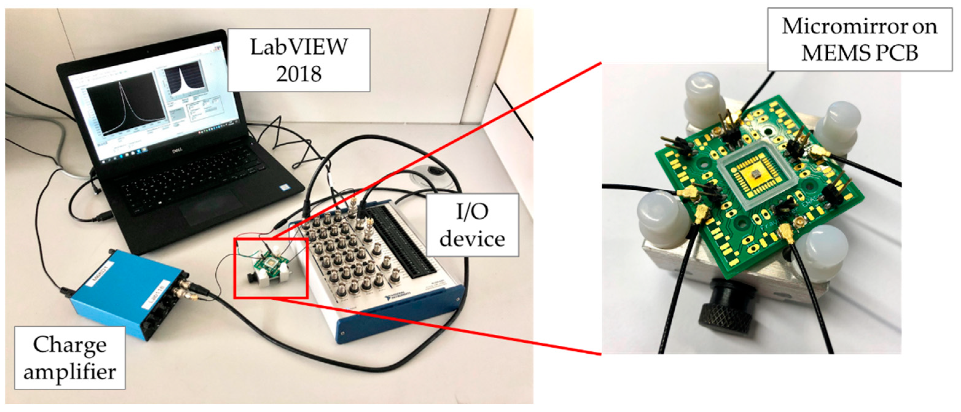
Figure 14.
Photograph of the sensor characterization setup.
Figure 14.
Photograph of the sensor characterization setup.
Figure 15.
Topological area scans of Design 1 performed using white light interferometry: (a) wafer center (Sample 1); (b) wafer edge (Sample 2).
Figure 15.
Topological area scans of Design 1 performed using white light interferometry: (a) wafer center (Sample 1); (b) wafer edge (Sample 2).
Figure 16.
Cross-section of the sample micromirrors (Design 1) of the wafer center (Sample 1) and the wafer edge (Sample 2). A zoomed section of the corresponding mirror plate is shown on the right.
Figure 16.
Cross-section of the sample micromirrors (Design 1) of the wafer center (Sample 1) and the wafer edge (Sample 2). A zoomed section of the corresponding mirror plate is shown on the right.
Figure 17.
Measurement points for displacement determination.
Figure 17.
Measurement points for displacement determination.
Figure 18.
Frequency response curve of an individual sample of Design 1 (recorded at Point 1).
Figure 18.
Frequency response curve of an individual sample of Design 1 (recorded at Point 1).
Figure 19.
Frequency response curve of an individual sample of Design 2 for x- and y-axis (recorded at Point 1 and 2, respectively).
Figure 19.
Frequency response curve of an individual sample of Design 2 for x- and y-axis (recorded at Point 1 and 2, respectively).
Figure 20.
Out-of-plane modes, measured by laser-Doppler-vibrometry for Design 1 and Design 2.
Figure 20.
Out-of-plane modes, measured by laser-Doppler-vibrometry for Design 1 and Design 2.
Figure 21.
Photograph of a micromirror at wafer level of Design 2 in operation at 50 V (approx. 30° mechanical tilt angle) captured by a single lens reflex (SLR) camera (Canon EOS 600D).
Figure 21.
Photograph of a micromirror at wafer level of Design 2 in operation at 50 V (approx. 30° mechanical tilt angle) captured by a single lens reflex (SLR) camera (Canon EOS 600D).
Figure 22.
Resonant scan angle versus actuation voltage: (a) Design 1 and Design 1-S; (b) Design 2. The y-axis error bar is the median absolute deviation.
Figure 22.
Resonant scan angle versus actuation voltage: (a) Design 1 and Design 1-S; (b) Design 2. The y-axis error bar is the median absolute deviation.
Figure 23.
Frequency ratio versus scan angle: (a) Design 1 and Design 1-S; (b) Design 2. The x- and y-axis error bar is the median absolute deviation.
Figure 23.
Frequency ratio versus scan angle: (a) Design 1 and Design 1-S; (b) Design 2. The x- and y-axis error bar is the median absolute deviation.
Figure 24.
Frequency response curves of Design 1: (a) Actuation with actuator pair A2 and A4 for different voltages; (b) Comparison of the frequency response curves, generated at actuation of A1 and A3 and A2 and A4 at 50 V.
Figure 24.
Frequency response curves of Design 1: (a) Actuation with actuator pair A2 and A4 for different voltages; (b) Comparison of the frequency response curves, generated at actuation of A1 and A3 and A2 and A4 at 50 V.
Figure 25.
Frequency response curves of Design 2: (a) x-axis; (b) y-axis.
Figure 25.
Frequency response curves of Design 2: (a) x-axis; (b) y-axis.
Figure 26.
Microscope image of a micromirror of Design 2. After sweeping the frequency resonance curve at 50 V, one of the 7.5 µm springs was broken after an undefined oscillation occurred.
Figure 26.
Microscope image of a micromirror of Design 2. After sweeping the frequency resonance curve at 50 V, one of the 7.5 µm springs was broken after an undefined oscillation occurred.
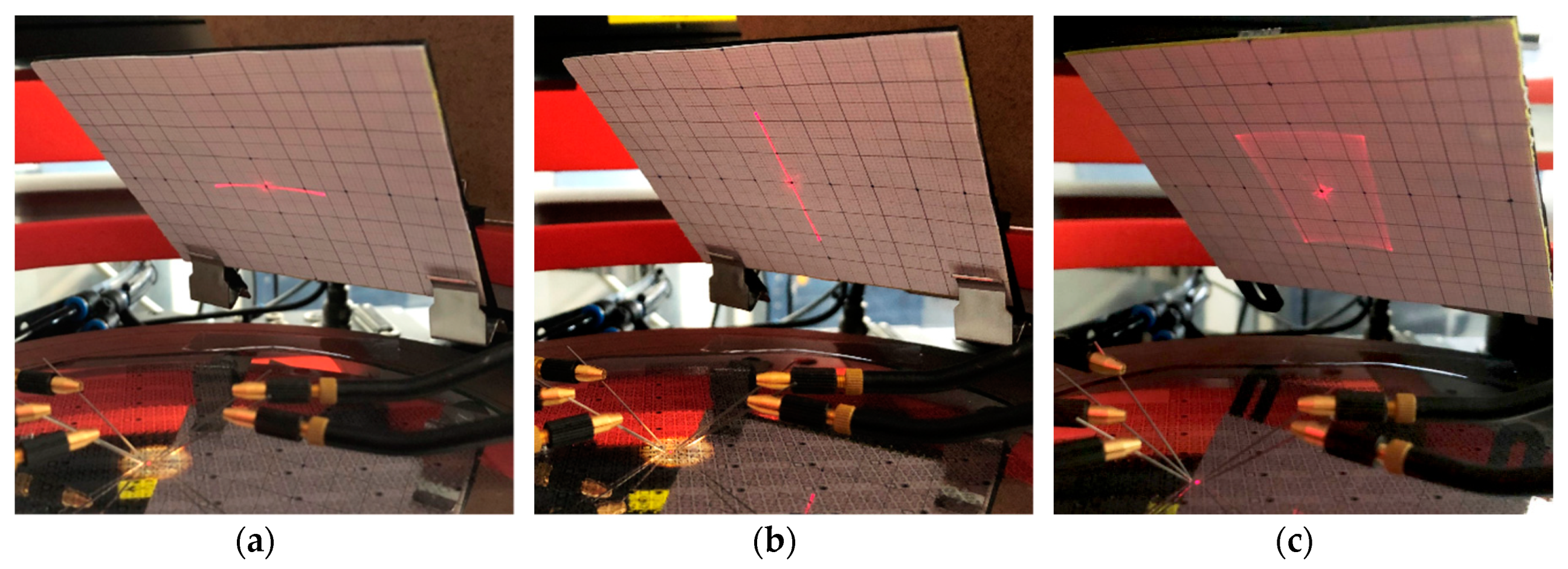
Figure 27.
Scan pattern of Design 1 at 10 V: (a) spiral scan line without amplitude modulation; (b) spiral scan pattern by amplitude modulation.
Figure 27.
Scan pattern of Design 1 at 10 V: (a) spiral scan line without amplitude modulation; (b) spiral scan pattern by amplitude modulation.
Figure 28.
Scan pattern of Design 2 at 10 V: (a) x-axis; (b) y-axis; (c) Lissajous scan pattern.
Figure 28.
Scan pattern of Design 2 at 10 V: (a) x-axis; (b) y-axis; (c) Lissajous scan pattern.
Figure 29.
Sensor output charge versus mechanical tilt angle for Design 1-S in resonant operation (average of four sensor elements). The x- and y-axis error bars are the measured median absolute deviations.
Figure 29.
Sensor output charge versus mechanical tilt angle for Design 1-S in resonant operation (average of four sensor elements). The x- and y-axis error bars are the measured median absolute deviations.
Table 1.
Overview of the designed spring widths in comparison to the resulting spring widths after fabrication. The target thickness of the device Si was 20 µm.
Table 1.
Overview of the designed spring widths in comparison to the resulting spring widths after fabrication. The target thickness of the device Si was 20 µm.
| Design | Design 1 | Design 1-S | Design 2 |
|---|
| x-Axis | y-Axis |
|---|
| Scan pattern | Spiral | Spiral | Lissajous |
| Designed spring width [µm] | 10 | 10 | 7.5 | 10 |
| Spring width after fabrication [µm] | 8.5 | 8.5 | 6.0 | 8.5 |
Table 2.
Parameter set for micromirror design and modeling [
18,
19,
20,
21,
22,
23].
Table 2.
Parameter set for micromirror design and modeling [
18,
19,
20,
21,
22,
23].
| Parameter | Axis | Designation | Unit | Si (111) | AlN | Al |
|---|
| Layer thickness | z | hz | µm | 20.0 | 0.6 | 0.5 |
| Young’s modulus | x | Ex | GPa | 168.9 | 308 | 68 |
| y | Ey | GPa | 168.9 | 308 | 68 |
| z | Ez | GPa | 168.9 | 308 | 68 |
| Shear modulus | x, y | Gxy | GPa | 66.9 | 128.3 | 28.6 |
| y, z | Gyz | GPa | 57.8 | 128.3 | 28.6 |
| x, z | Gxz | GPa | 57.8 | 128.3 | 28.6 |
| Poisson number | x, y | νxy | | 0.262 | 0.2 | 0.32 |
| x, z | νxz | | 0.182 | 0.2 | 0.32 |
| y, z | νyz | | 0.182 | 0.2 | 0.32 |
| Piezoelectric coefficient | | d31 | pm/V | - | −2 | - |
Table 3.
Actuator excitation parameters to generate the corresponding scan patterns.
Table 3.
Actuator excitation parameters to generate the corresponding scan patterns.
| Actuator | Analog Output | Spiral | Lissajous |
|---|
| x-Axis | y-Axis |
|---|
| A1 | AO0 | fx = fy, φ = 0° | - | f = fy, φy = 0° |
| A2 | AO1 | fx = fy, φ = 90° | f = fx, φx = 0° | - |
| A3 | AO2 | fx = fy, φ = 180° | - | f = fy, φy = 180° |
| A4 | AO3 | fx = fy, φ = 270° | f = fx, φx = 180° | - |
Table 4.
Comparison of finite elements (FE) simulation and laser-Doppler-vibrometry (LDV) measurement of Design 1.
Table 4.
Comparison of finite elements (FE) simulation and laser-Doppler-vibrometry (LDV) measurement of Design 1.
| Parameters | Unit | Measurement Point | FE Simulation 1 | LDV Measurement 2 | Measurement Uncertainty |
|---|
| (Quasi)static deflections |
| Mirror deflection | nm/V | 1, 2 | 12 | 10.6 | 0.3 |
| Actuator deflection | nm/V | 4 | 34 | 29.4 | 0.7 |
| nm/V | 5 | 25 | 20.8 | 1.3 |
| Resonant deflections (tilt mode) |
| Quality factor | | 1, 2 | - | 214 | 0.6 |
| Mirror deflection | nm/V | 1, 2 | - | 2361 | 189 |
| Mech. Tilt angle | °/V | 1, 2 | - | 0.39 | 0.03 |
| Actuator deflection | nm/V | 4 | - | 1499 | 259 |
| nm/V | 5 | - | 1108 | 214 |
| Resonance Frequencies |
| Piston mode | Hz | 3 | 8315 | 8263 | 175 |
| Tilt mode | Hz | 1, 2 | 14,139 | 14,066 | 265 |
| Actuator mode | Hz | 4 | 19,835 | 19,809 | 367 |
Table 5.
Comparison of FE simulation 1 and LDV measurement of Design 1-S.
Table 5.
Comparison of FE simulation 1 and LDV measurement of Design 1-S.
| Parameters | Unit | Measurement Point | FE Simulation 1 | LDV Measurement 2 | Measurement Uncertainty |
|---|
| (Quasi)static deflections |
| Mirror deflection | nm/V | 1, 2 | 6.0 | 4.3 | 0.2 |
| Actuator deflection | nm/V | 4 | 17.1 | 14.8 | 0.7 |
| nm/V | 5 | 12.3 | 8.5 | 0.5 |
| Resonant parameters (tilt mode) |
| Quality factor | | 1, 2 | - | 223 | 8.4 |
| Mirror deflection | nm/V | 1, 2 | - | 1012 | 40.9 |
| Mech. Tilt angle | °/V | 1, 2 | - | 0.17 | 0.01 |
| Actuator deflection | nm/V | 4 | - | 596 | 14.5 |
| nm/V | 5 | - | 439 | 14.8 |
Table 6.
Comparison of FE simulation and LDV measurement of Design 2.
Table 6.
Comparison of FE simulation and LDV measurement of Design 2.
| Parameters | Unit | Measurement Point | FE Simulation 1 | LDV Measurement 2 | Measurement Uncertainty |
|---|
| | | | x-axis | y-axis | x-axis | y-axis | x-axis | y-axis |
| (Quasi)static deflections |
| Mirror deflection | nm/V | 1, 2 | 9.2 | 14.2 | 6.9 | 13.9 | 0.3 | 0.4 |
| Actuator deflection | nm/V | 4 | 33 | 33 | 29.1 | 29.1 | 0.7 | 0.8 |
| nm/V | 5 | 26 | 26 | 19.3 | 20.2 | 0.4 | 1.3 |
| Resonant deflections (tilt mode) |
| Quality factor | | 1, 2 | - | - | 281 | 219 | 10.2 | 7.8 |
| Mirror deflection | nm/V | 1, 2 | - | - | 2408 | 2642 | 126.2 | 98.1 |
| Mech. Tilt angle | °/V | 1, 2 | - | - | 0.39 | 0.43 | 0.02 | 0.02 |
| Actuator deflection | nm/V | 4 | - | - | 740 | 1287 | 182 | 61 |
| nm/V | 5 | - | - | 460 | 949 | 87 | 55 |
| Resonance Frequencies |
| Piston mode | Hz | 3 | 7491 | - | 7438 | - | 123 | - |
| Tilt mode | Hz | 1, 2 | 12,140 | 13,738 | 12,131 | 13,549 | 208 | 249 |
| Actuator mode | Hz | 4 | 18,261 | 20,043 | 18,016 | 19,799 | 111 | 379 |
Table 7.
Comparison of resonant driven micromirrors based on piezoelectric AlN in the current literature and this work.
Table 7.
Comparison of resonant driven micromirrors based on piezoelectric AlN in the current literature and this work.
| Specification | Unit | J. Shao [6] | K. Meinel [10] | This Work |
|---|
| Design 1-S | Design 2 |
|---|
| Mirror plate area | mm2 | 0.04 | 0.64 | 0.5 | 0.5 |
| Chip size | mm2 | - | 6 | 4 | 4 |
| Drive frequency | kHz | 63.3 | 3.4 | 14.1 | 12.1, 13.1 |
| Drive voltage | V | 5 | 20 | 50 | 50 |
| Scan angle | ° | 4.0 | 137.9 | 60.2 | 92.4, 123.9 |
| Sensor angle sensitivity | pC/° | - | 0.05 | 1.7 | - |
| Number of scan dimensions | | 2 | 1 | 2 | 2 |

 ,
, 


