1. Introduction
A light-addressable potentiometric sensor (LAPS) [
1,
2,
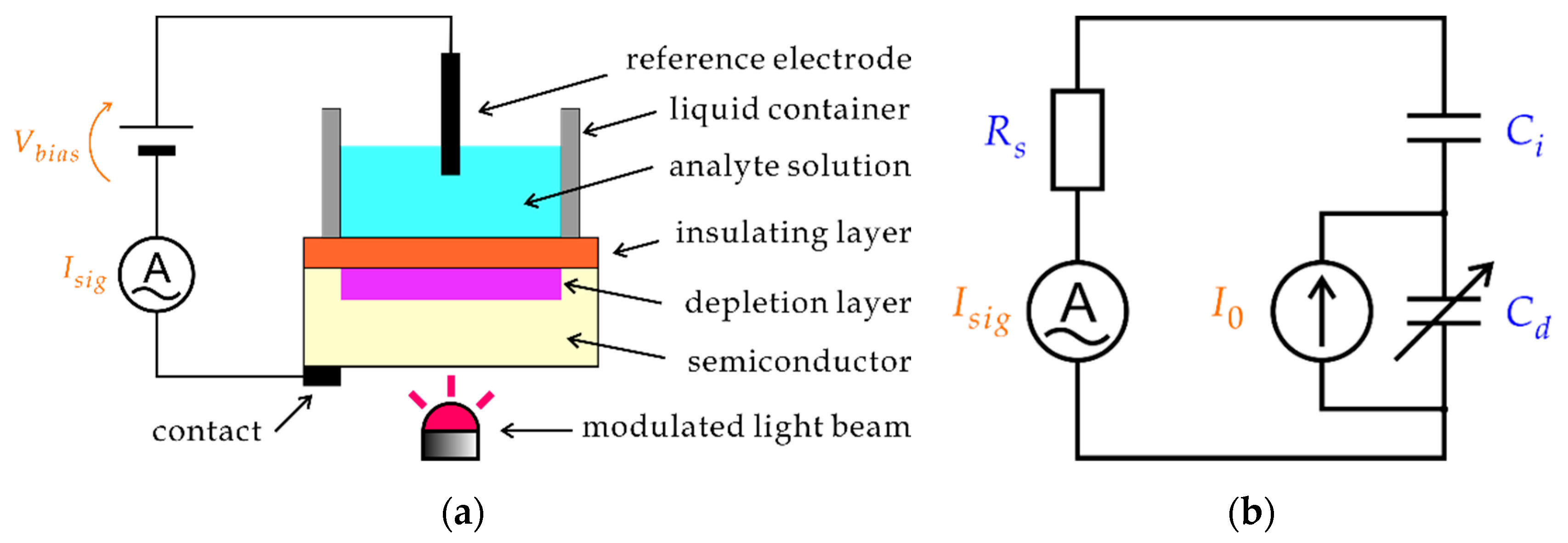
3] is a semiconductor-based chemical sensor, which has a field-effect structure shown in
Figure 1a. A dc voltage is applied to induce a depletion layer, the thickness of which varies due to the field effect in response to the analyte concentration on the sensing surface. A photocurrent generated by illuminating the semiconductor is measured to detect the variation of the capacitance of the depletion layer and to determine the analyte concentration. A spatially resolved measurement is possible by using a scanning light beam, which is the basis of the chemical imaging sensor [
3,
4] and the scanning photo-induced impedance microscopy [
5].
In theoretical analysis of a LAPS, a simple circuit model, shown in
Figure 1b, has been conventionally employed [
6,
7,
8]. In this model, separation of electrons and holes by the electric field inside the depletion layer is represented by an internal ac current source
, which is divided by the capacitance of the depletion layer
and that of the insulating layer
connected to the series resistance of the circuit
. Here,
consists of the resistance of the solution between the illuminated point and the reference electrode, the resistance of the reference electrode (in case the counter electrode is not used), the input resistance of the ammeter, and the contact resistance on the back surface of the semiconductor substrate. When the thickness of the depletion layer changes in response to the analyte concentration of the solution in contact with the sensing surface, variation of
results in variation of the signal current
. This circuit model was further combined with the carrier diffusion model [
8,
9,
10,
11,
12,
13] to describe the operation of the chemical imaging sensor, taking account of lateral diffusion and recombination of minority carriers inside the semiconductor substrate.
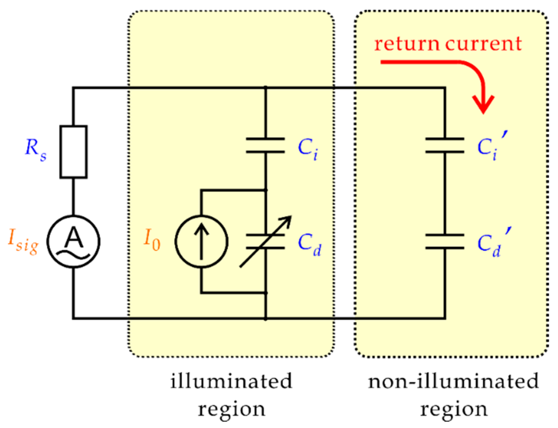
Although these models were successful in describing important features of the chemical imaging sensor including its spatial resolution and frequency characteristics, Poghossian et al. [
14] pointed out the influence of capacitive coupling between the solution and the semiconductor substrate in the non-illuminated region, which was not included in existing models.
Figure 2 shows the simplest model, in which a part of the ac current returns to the semiconductor substrate through
and
without contributing to the signal current
. It should be noted that this effect applies only to an ac current. In light-activated electrochemistry (LAE) [
15], which has a similar setup to that of LAPS but uses dc faradaic current, the high impedance of the non-illuminated region separates the solution and the substrate.
Figure 2 gives only an intuition that the capacitive coupling increases with the area of the non-illuminated region and the frequency of the ac current. It can be easily speculated that a loss of the signal current due to the return current may have a large impact on the signal-to-noise ratio, the spatial resolution, and the sensitivity. To be able to understand the dependence of the return current on various parameters and to evaluate its impact on the sensor performance, the model shown in
Figure 2 is far too simple.
In this study, a new circuit model is proposed, in which the path of the return current is described as a transmission line. The model is used to calculate the influence of the return current on and its dependence on parameters such as the frequency, the size of the non-illuminated region, the conductivity of the solution, and the series resistance of the circuit. Applicability and limitation of the model are discussed by comparing the results obtained by calculation and measurement.
2. Model
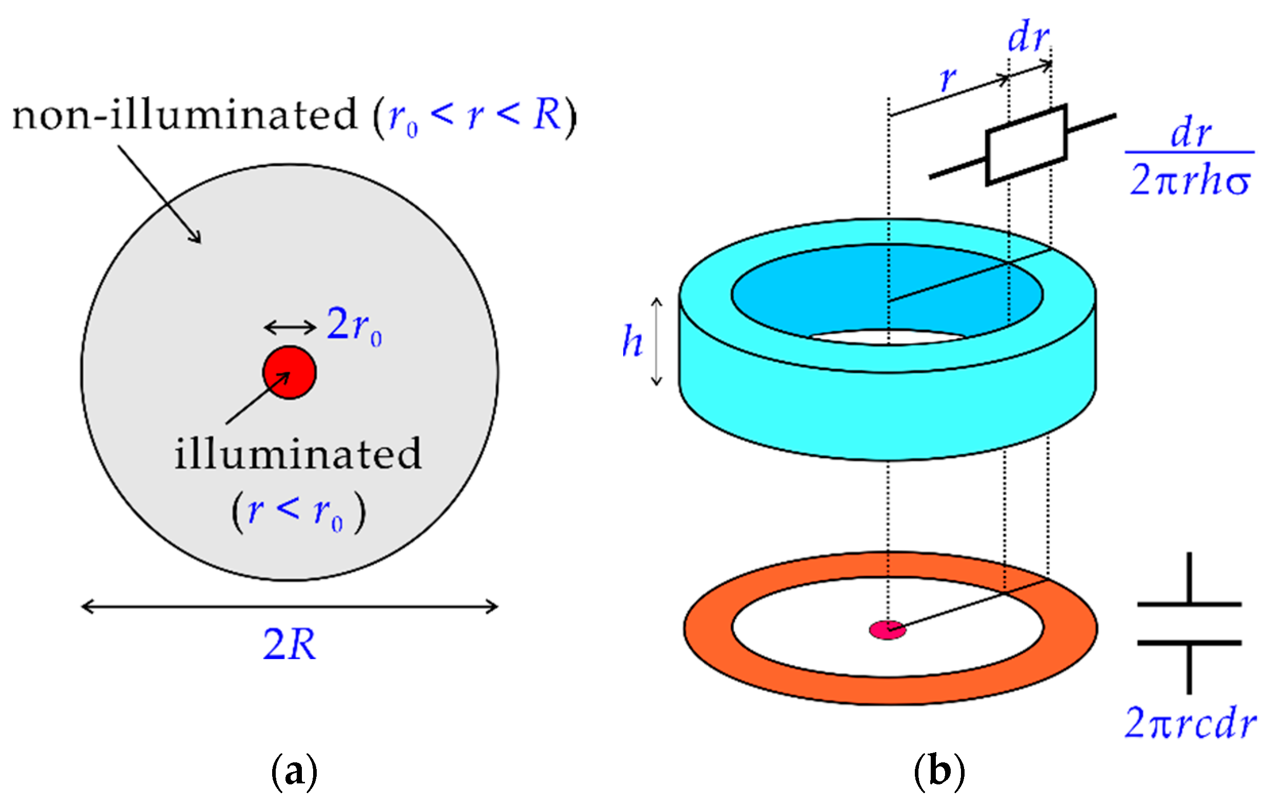
Figure 3a shows the top view of the model, in which a circular region on the sensing surface with a radius
is in contact with the solution and a circular region with a radius
at the center is illuminated. The rest of the contact area (
) is non-illuminated. The resistance of the solution in an infinitesimal volume between the inner and outer walls of a hollow cylinder with a radius
and a thickness
shown in the upper part of
Figure 3b is given by:
where
is the height of the solution and
is the specific conductivity of the solution. The combined capacitance of the insulating layer and the depletion layer in an infinitesimal area between
and
shown in the lower part of
Figure 3b is given by
where
is the combined capacitance per unit area. When the capacitance of the insulating layer per unit area
and that of the depletion layer
are connected in series, the combined capacitance is given by
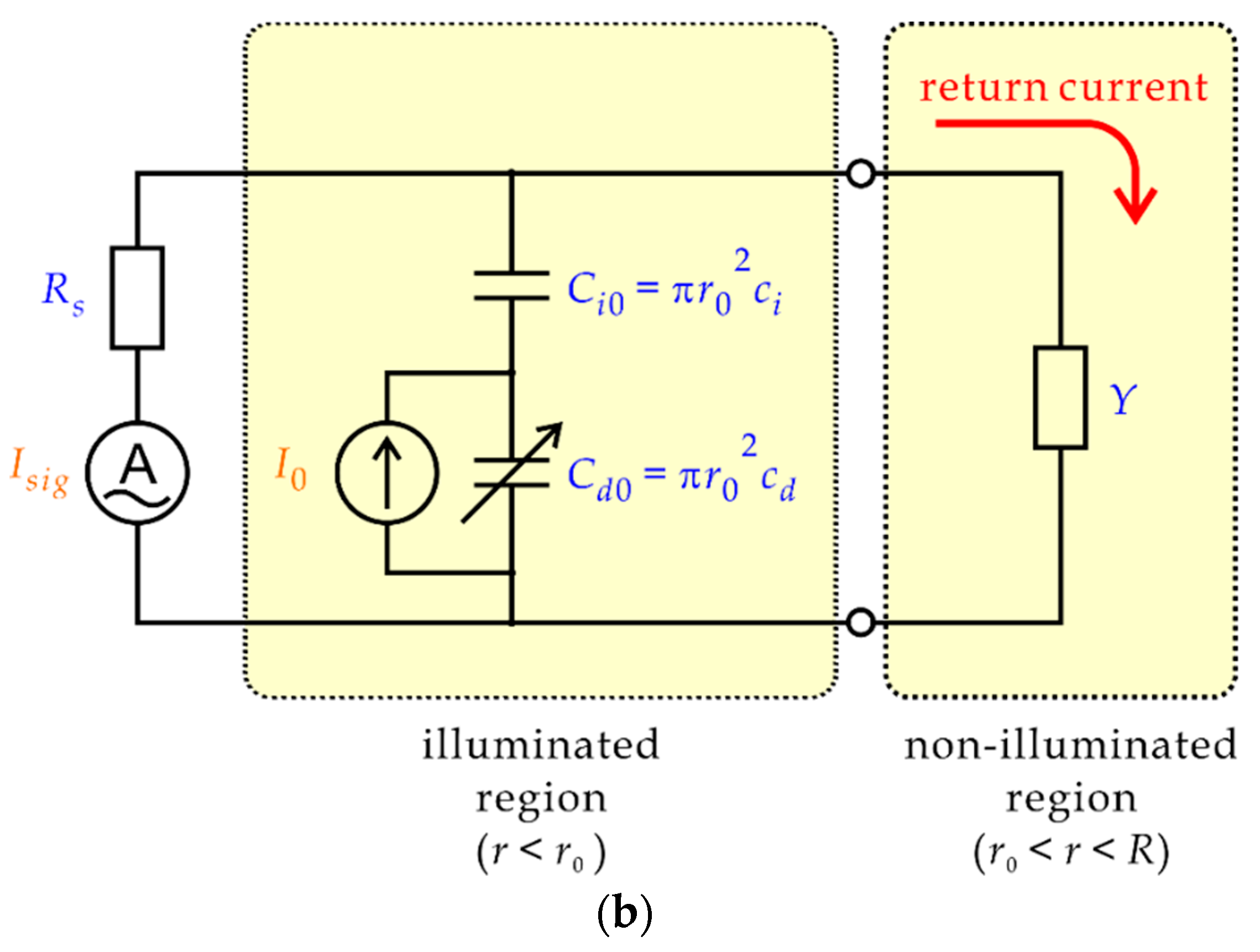
The admittance of the non-illuminated region
is represented as a ladder network shown in
Figure 4a, which is essentially a finite-length transmission line with an open end. Unlike a conventional transmission line, however, the resistance and the capacitance per unit length are not constant but dependent on
as described by (1) and (2), respectively. The telegraph equations of the transmission line are
where
and
are complex numbers representing the phasors of the ac current and the ac voltage with an angular frequency
(
) at position
and
is the imaginary unit. From Equations (4a) and (4b) we obtain a second-order ordinary differential equation,
where
By solving Equation (5) under initial conditions at
, we can obtain final values
and
. Then, we also obtain
from Equation (4a), and the input admittance
in
Figure 4b is given by
Once
is obtained, the signal current
can be calculated as follows.
Here,
is the capacitance of the insulating layer inside the illuminated region and
is that of the depletion layer, which are given by
The initial conditions at
are given as follows. Since the current does not flow out of the contact area,
The value of
, or equivalently the value of
, can be arbitrarily given, as we are interested only in the ratio of
and
. For simplicity, we choose it to be
For ease of calculation, the second-order ordinary differential equation of a complex-valued function (5) can be converted into a set of first-order ordinary differential equations of four real-valued functions by defining
Then, our problem is to solve a set of differential equations
under the initial conditions
Finally, we obtain the values
,
,
, and
, which give
In the following sections, calculations were done by a Runge–Kutta solver
ode45 of MATLAB
® (MathWorks). Parameters listed in
Table 1 were used so that the results of calculation can be compared with those experimentally obtained.
3. Dependence on and
First of all, the dependence of the admittance
on the radius of the non-illuminated region
and the frequency
was calculated as summarized in
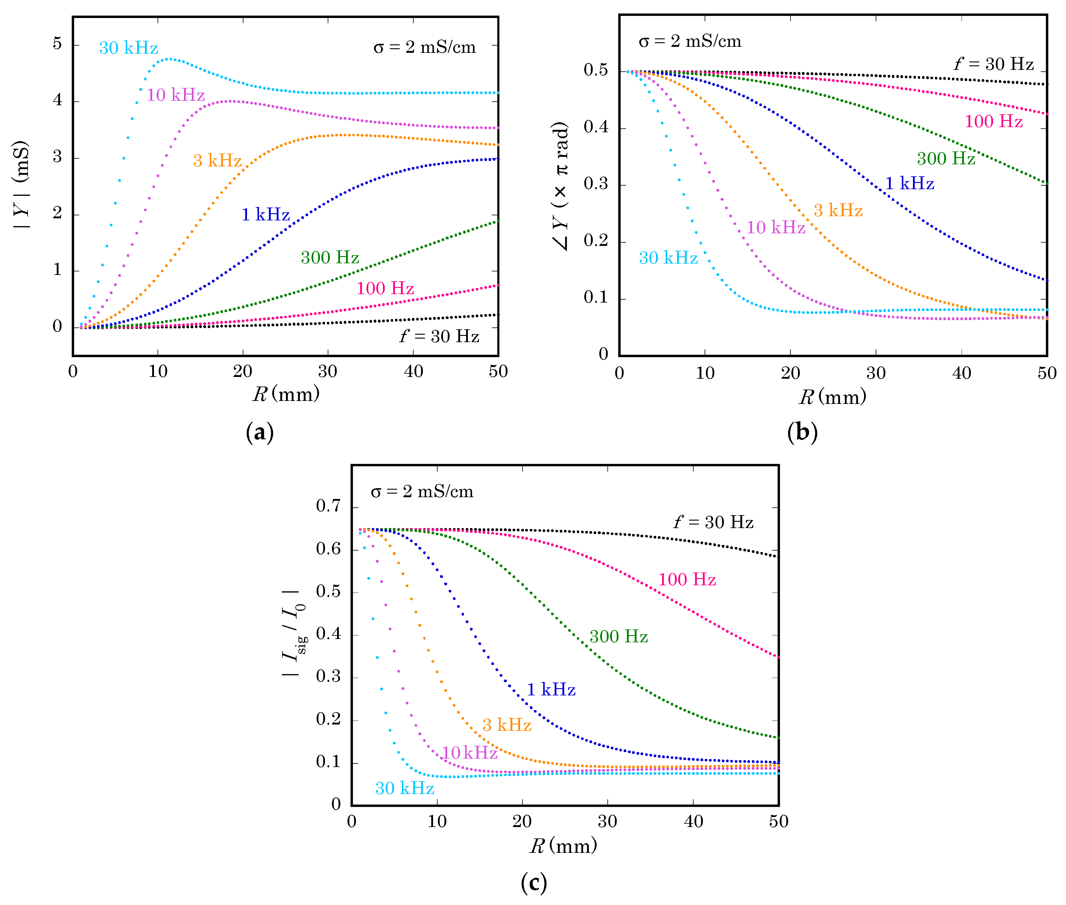
Figure 5.
Figure 5a shows the magnitude of
calculated with the model described in the previous section. As expected, the magnitude of
becomes larger at higher frequencies, meaning that more current returns from the solution to the semiconductor substrate through their capacitive coupling. Moreover, the magnitude of
becomes larger as
increases and the contact area becomes larger. However, the admittance of a finite-length transmission line does not always increase monotonously with its length. In fact, curves for the frequency of 3 kHz and higher have maxima.
In
Figure 5b, the argument of
is plotted as a function of
. When the contact area is small, the transmission line is mostly capacitive, and it becomes more resistive as
increases. This behavior is qualitatively understood as follows. When
increases, more portion of the return current flows through the capacitance at locations further from the center, in other words, after going through a larger lateral resistance of the solution on the way. At higher frequencies, this transition of the argument of
occurs at smaller distance
.
Figure 5c shows the magnitude of
as a function of
at different frequencies. As
increases, the admittance of the non-illuminated region
becomes larger and the signal current decreases due to the increase of the return current. In the present case, where calculation was done with parameters listed in
Table 1, the signal current decreased down to about 14% of the value at
, where the non-illuminated region does not exist.
4. Dependence on and
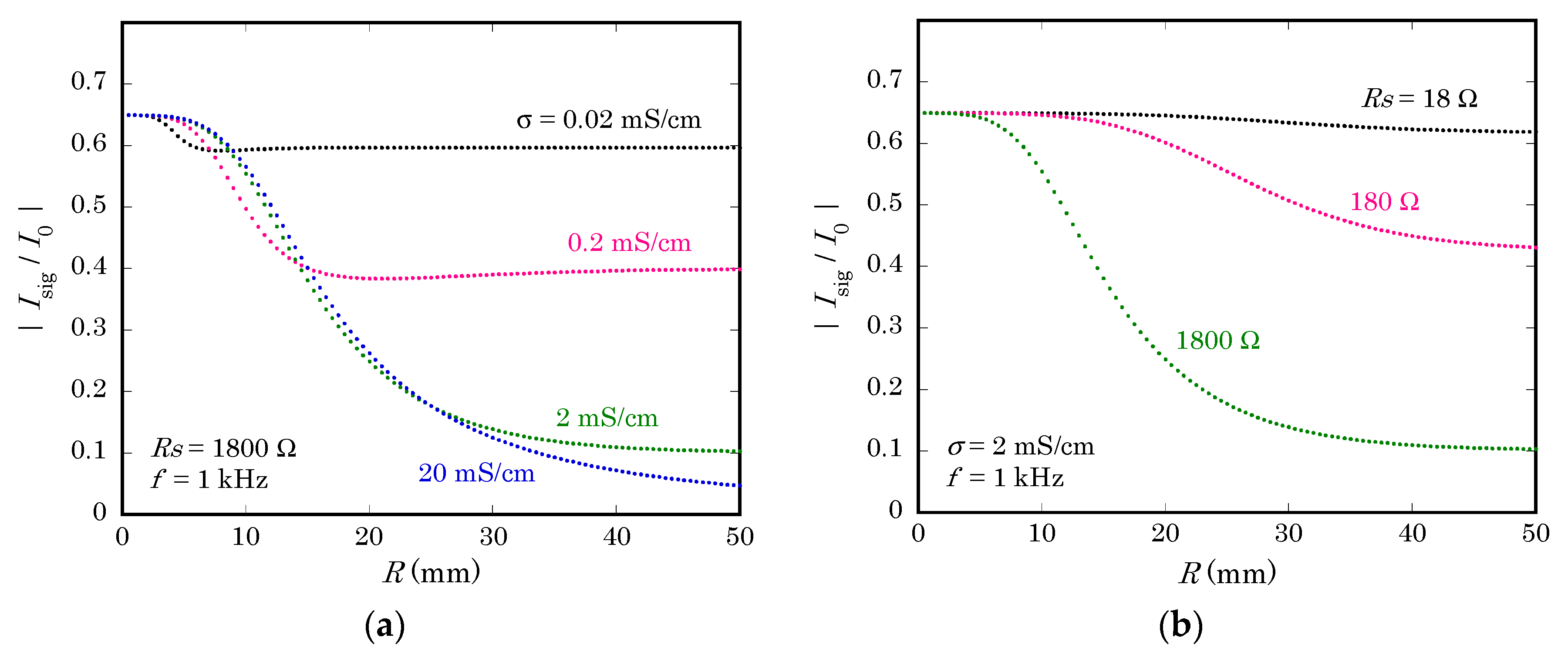
In
Figure 6a, the dependence of the signal current
on the radius of the non-illuminated region
is plotted for different values of the specific conductivity of the solution
. Here, the series resistance of the circuit
and the frequency
were kept constant at 1800 Ω and 1 kHz, respectively. When the solution is less conductive, the effect of the return current is relatively smaller, because the lateral resistance will limit the distance from the center, within which the capacitive coupling contributes to the return current. It should be noted, however, that a smaller conductivity of the solution also implies a higher resistance of the solution between the illuminated point and the reference electrode, which increases
. As a whole, therefore, less conductivity will not necessarily reduce the effect of the return current.
In
Figure 6b, calculation was done for different values of
, while keeping
and
at 2 mS/cm and 1 kHz, respectively. It clearly shows that reduction of
is of utmost importance in removing the effect of the return current. To reduce
, a three-electrode system with a counter electrode should be used to bypass the resistance of the reference electrode. The electronic circuit to collect the ac photocurrent signal, typically a transimpedance amplifier based on operational amplifiers, should be carefully designed to minimize its input impedance. The ohmic contact on the back surface of the semiconductor substrate must be carefully formed to minimize the contact resistance.
In some applications, a planer counter electrode can be placed in parallel to the sensing surface, so that the vertical distance from the illuminated point to the counter electrode is always small and constant even when the position of the light beam is moved for scanning. In case of measurement inside a microfluidic device, a metallic wire can be inserted along the microchannel as a counter electrode. In these cases, the counter electrode helps, on one hand, to reduce , but it also shortcuts the lateral resistance of the solution and delivers the return current to locations far from the illuminated point and may increase the return current.
5. Impact on the Sensitivity
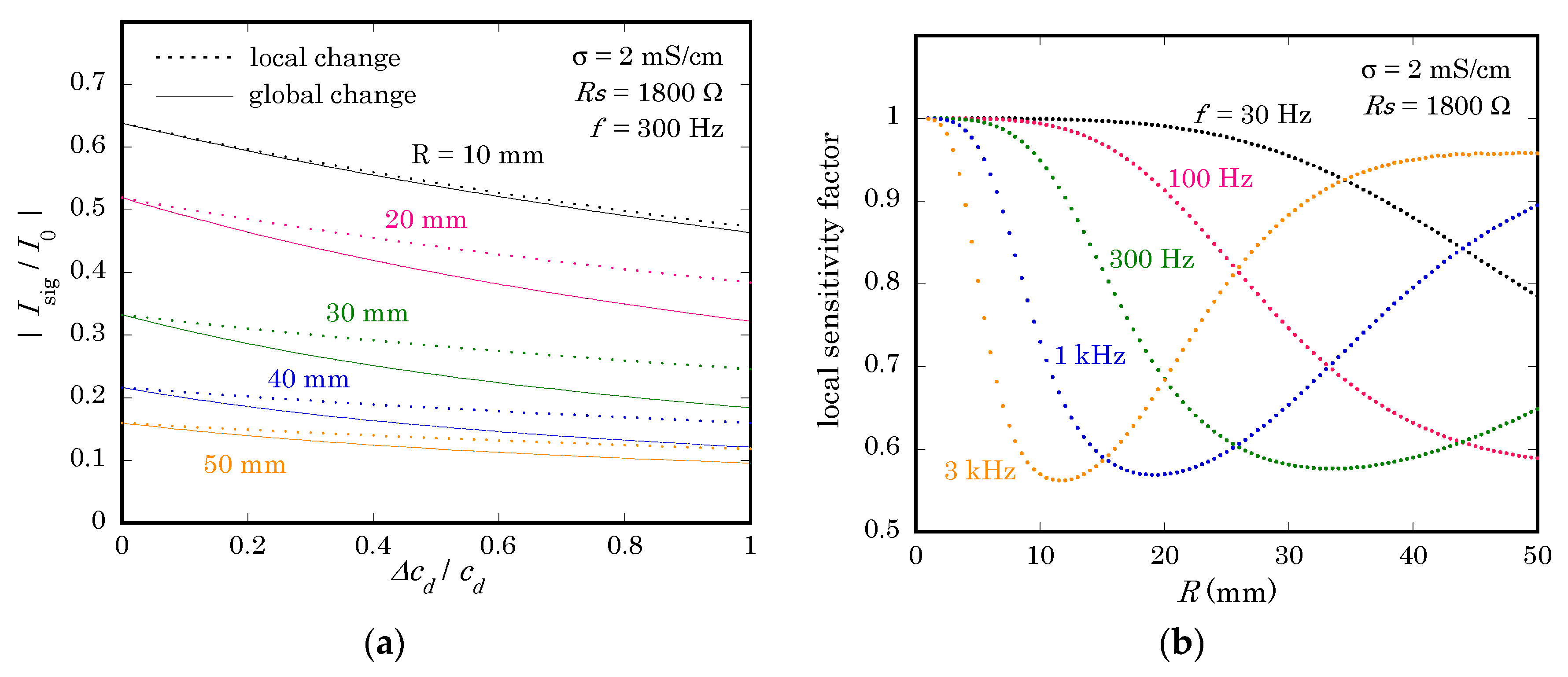
In chemical imaging based on a LAPS, a focused light beam scans the semiconductor substrate, and the signal current is recorded at each pixel. The signal current is then converted into the analyte concentration using a calibration curve acquired prior to the measurement. For a small change, a linear approximation is used to convert a variation of the signal current into that of the potential, which is then linearly correlated to the logarithm of the activity of the analyte using the Nernst equation.
Under the existence of a return current, however, this conversion may be systematically affected due to the following reason. During the calibration step, the entire sensing surface is uniformly in contact with known concentrations of analyte solutions. In such a case, the thickness of the depletion layer varies equally both in the illuminated region and in the non-illuminated region, and varies under the global change of . During the measurement step, however, may change only locally, and the return current may be different from that in the calibration step.
To illuminate the difference, calculation was carried out in two different situations. First,
was calculated while changing
both in the illuminated region and in the non-illuminated region, which corresponds to the situation of the calibration step. Second,
was calculated while changing
only in the illuminated region with
in the non-illuminated region unchanged.
Figure 7a shows, for different values of
, the variation of
as a function of
in the range of 0 to 1. It is clearly observed that the variation of
for a local change of
is smaller than that for a global change of
. In other words, a local change of the analyte concentration in imaging will be underestimated due to the difference of the return current during calibration and measurement.
The ratio of the slope (calculated in the range between
= 0 and 1) for a local change of
in
Figure 7a and that for a global change of
was defined as a local sensitivity factor, which indicates the degree of underestimation.
Figure 7b shows the local sensitivity factor as a function of
at different frequencies. This result shows that a local change can be underestimated, depending on the combination of
and
, by a factor even smaller than 0.6 in the calculated case, where
was 1800 Ω. When
was reduced to 18 Ω, the local sensitivity factor calculated within the same range of conditions as in
Figure 7b was always larger than 0.96 (data not shown), meaning that the underestimation was less than 4%. This result again shows the importance of reducing
in removing the effect of the return current in a LAPS.
6. Comparison with Experiments
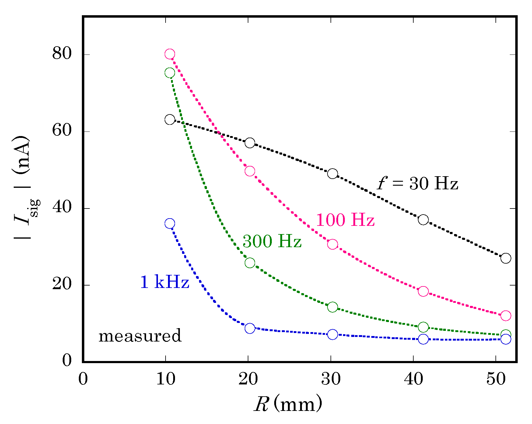
A series of experiments were carried out to observe the dependence of on and in a real situation. A large-area LAPS plate was prepared by depositing 50 nm SiO2 and 50 nm Si3N4 successively on the entire surface of a 6-inch n-type Si wafer with a thickness of 200 μm and a resistivity of 1–10 Ωcm. An ohmic contact was evaporated on the perimeter of the back surface. To define different sizes of contact areas between the solution and the sensing surface, various sizes of cylindrical liquid containers to accommodate the solution were prepared by a 3D printer and attached to the sensing surface via O-rings with inner diameters 21.0, 40.5, 60.5, 82.5, and 102.5 mm. The solution used in this experiment was 0.1 wt% NaCl solution with a specific conductivity = 2.0 mS/cm and the height was = 10 mm. A Ag/AgCl reference electrode (RE-1B, BAS Inc.) was dipped into the solution at the center.
The capacitance of the insulating layer per unit area and the series resistance of the circuit were determined by the following method. A coil with an inductance 100 mH was inserted in the circuit and the sensor was biased at = +1.0 V, where the depletion layer disappears. For each size of the contact area, the ac current in response to the application of a small ac voltage was recorded to find the resonance peak while scanning the frequency. The capacitance was calculated from the peak position, and the series resistance was calculated from the peak height. Then, the value of was determined to be F/m2 by linear regression of the capacitance versus the contact area, and the average value of was Ω. The measured value of was close to F/m2, a theoretical value for a double layer comprising 50 nm SiO2 and 50 nm Si3N4. The capacitance of the depletion layer per unit area at = −2.0 V was determined to be F/m2 by linear regression of the measured capacitance versus the contact area. The measured value of was close to F/m2, a theoretical value for n-type Si with a donor concentration cm−3 under strong inversion at 300 K.
A LAPS signal was collected at
= −2.0 V by illuminating the center of the back surface with a modulated light beam from a red LED. The radius of illumination was restricted to 0.5 mm by an aperture.
Figure 8 shows the magnitude of the ac current signal for different values of
and
. Here, it should be noted that the vertical axis of
Figure 8 is not normalized, while the magnitude of
in
Figure 5c is normalized to
, which depends on the frequency but cannot be directly measured in experiments. The similar dependence of curves on
and
in
Figure 5c and
Figure 8 proves that the loss of the current signal is qualitatively reproduced by calculating the return current using the proposed model.
A closer look at concavity of curves reveals that there is a discrepancy of frequencies by a factor of 2 to 3 between curves of corresponding shapes in
Figure 5c and
Figure 8. A possible reason of this discrepancy is the different waveforms of the ac photocurrent in calculation and experiments. While the calculation assumes an internal current source
producing a sinusoidal waveform with a single frequency, the light beam used in an experiment is turned on and off at a certain frequency, which produces sinusoidal waveforms only at higher frequencies. When the frequency is relatively low, a transient current flows only for a short period after the light beam is turned on or off. The resulting waveform is distorted and contains higher frequency components [
13], for which the susceptance becomes larger, and the return current will be larger than calculated.
The waveform of a LAPS current signal can be reproduced by a device simulation, which takes account of the dynamics of minority carriers inside the semiconductor layer [
13]. For more precise estimation of the return current, therefore, combination of a circuit model and device simulation should be considered.
7. Conclusions
In this study, a circuit model for the return current in a LAPS was proposed, where the conductivity of the solution and the capacitive coupling between the solution and the semiconductor substrate in the non-illuminated region were formulated as a transmission line. The telegraph equation was numerically solved to find the input admittance of the non-illuminated region, and the dependence of the signal current on various parameters such as the diameter of contact area, the modulation frequency, the specific conductivity of the solution, and the series resistance of the circuit was investigated. It was found that a local change of the analyte concentration in imaging may be underestimated because of the difference of the return current in calibration and in measurement. The dependence of the LAPS signal current on the contact area and the frequency was also observed in experiments, which was compared with the calculated results.

 ,
, 

