Real-Space Probing of the Local Magnetic Response of Thin-Film Superconductors Using Single Spin Magnetometry

 , ,
, , 
Abstract
:1. Introduction
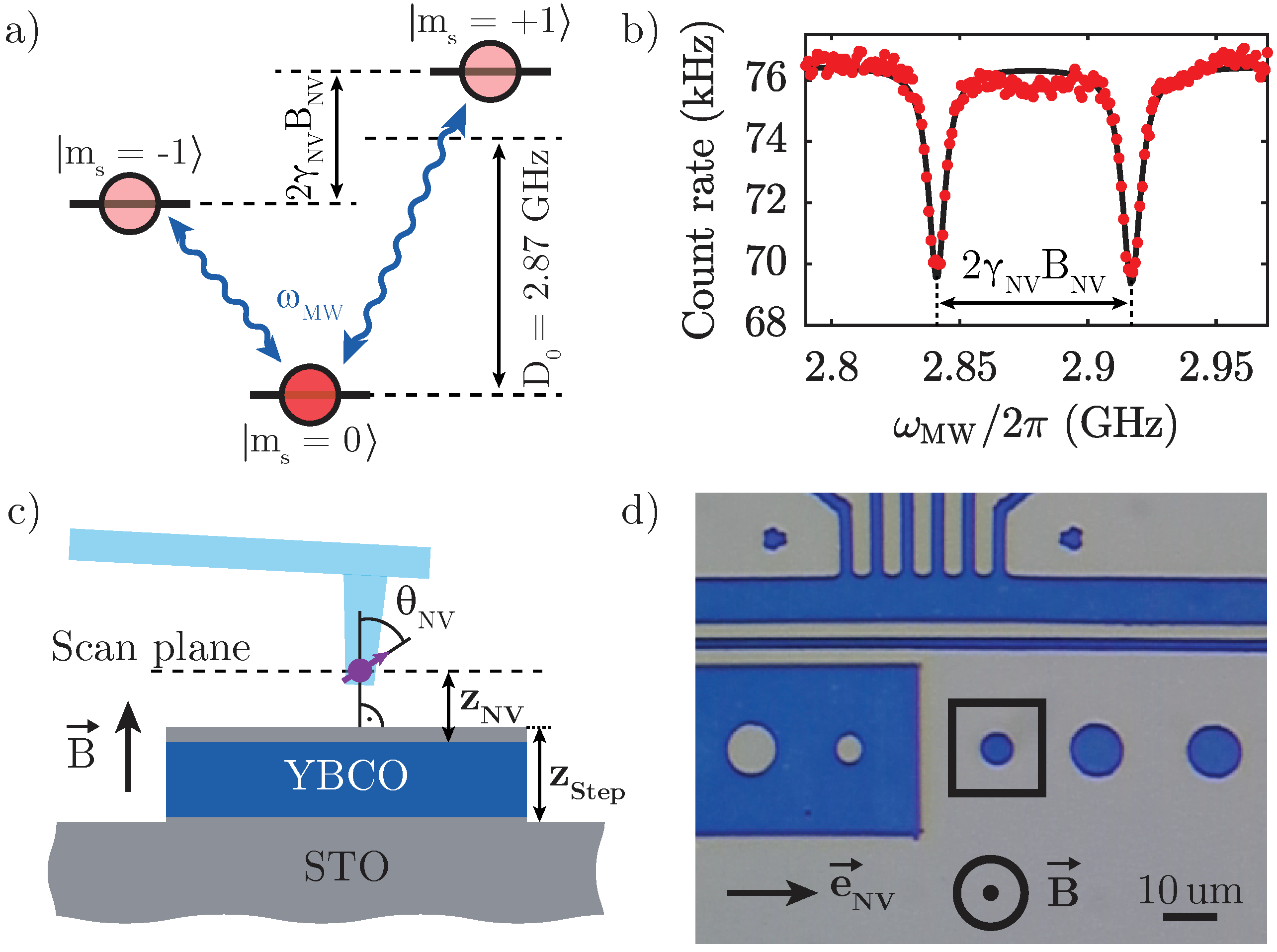
2. Experiment
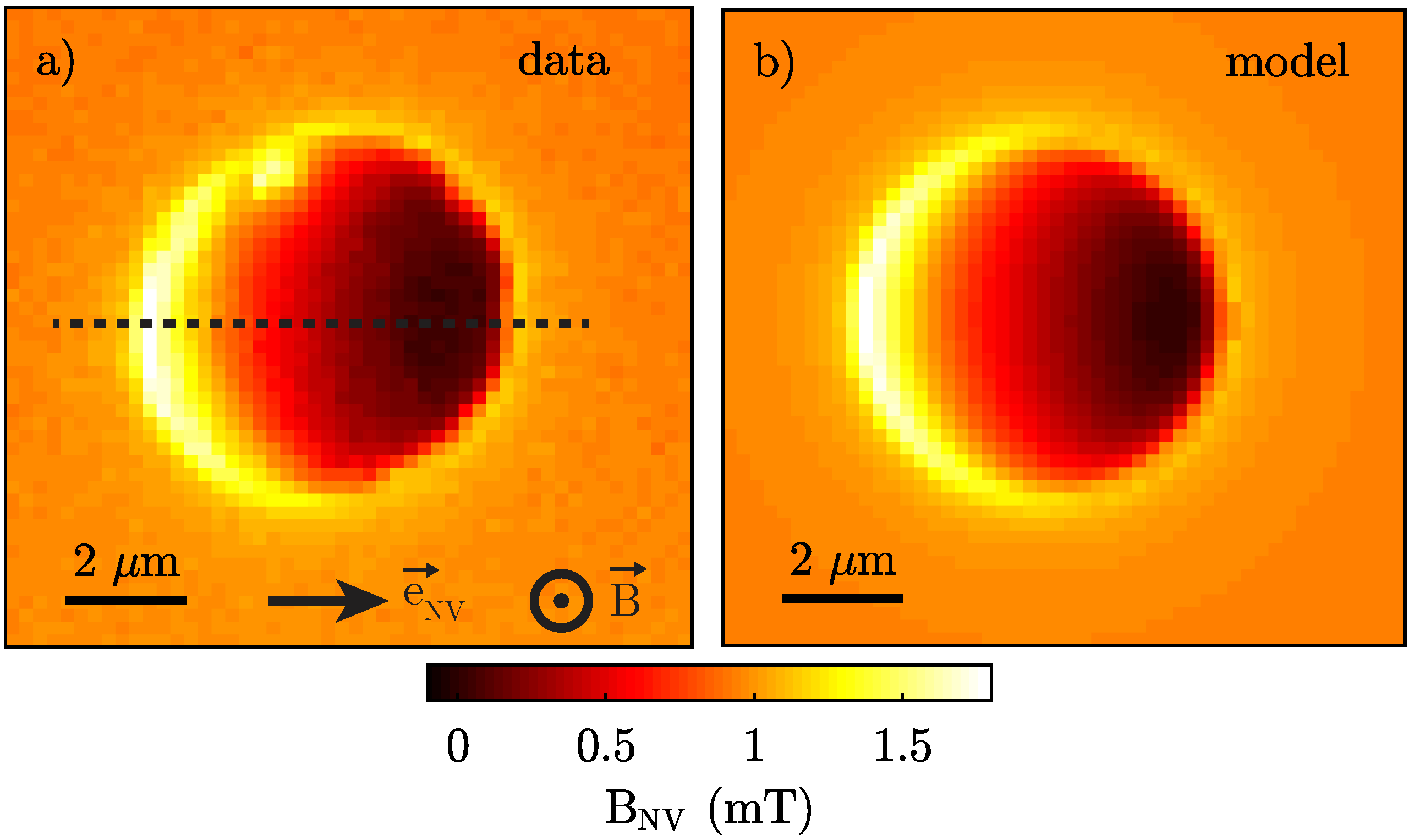
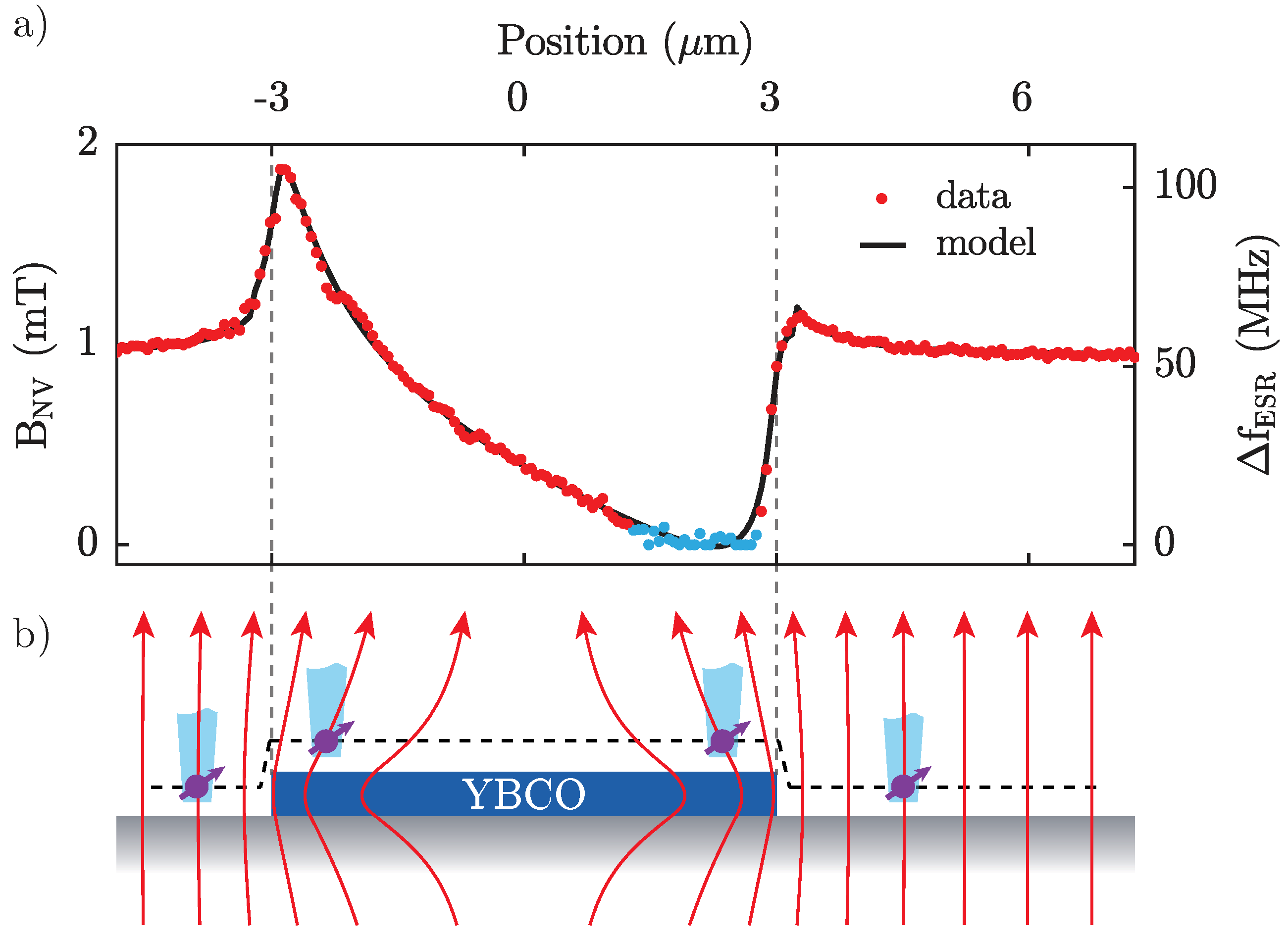
3. Results and Discussion
4. Conclusions and Summary
Author Contributions
Funding
Acknowledgments
Conflicts of Interest
References
- Božović, I.; He, X.; Wu, J.; Bollinger, A.T. Dependence of the critical temperature in overdoped copper oxides on superfluid density. Nature 2016, 536, 309–311. [Google Scholar] [CrossRef] [PubMed]
- Caviglia, A.D.; Gariglio, S.; Reyren, N.; Jaccard, D.; Schneider, T.; Gabay, M.; Thiel, S.; Hammerl, G.; Mannhart, J.; Triscone, J.M. Electric field control of the LaAlO3/SrTiO3 interface ground state. Nature 2008, 456, 624–627. [Google Scholar] [CrossRef] [PubMed]
- Wendin, G. Quantum information processing with superconducting circuits: A review. Rep. Prog. Phys. 2017, 80, 106001. [Google Scholar] [CrossRef] [PubMed]
- Müller, C.; Cole, J.H.; Lisenfeld, J. Towards understanding two-level-systems in amorphous solids-Insights from quantum devices. arXiv, 2017; arXiv:1705.01108. [Google Scholar]
- Dauler, E.A.; Grein, M.E.; Kerman, A.J.; Marsili, F.; Miki, S.; Nam, S.W.; Shaw, M.D.; Terai, H.; Verma, V.B.; Yamashita, T. Review of superconducting nanowire single-photon detector system design options and demonstrated performance. Opt. Eng. 2014, 53, 081907. [Google Scholar] [CrossRef] [Green Version]
- Badía, A.; Freyhardt, H.C. Meissner state properties of a superconducting disk in a non-uniform magnetic field. J. Appl. Phys. 1998, 83, 2681–2688. [Google Scholar] [CrossRef]
- Kim, J.; Civale, L.; Nazaretski, E.; Haberkorn, N.; Ronning, F.; Sefat, A.S.; Tajima, T.; Moeckly, B.H.; Thompson, J.D.; Movshovich, R. Direct measurement of the magnetic penetration depth by magnetic force microscopy. Supercond. Sci. Technol. 2012, 25, 112001. [Google Scholar] [CrossRef] [Green Version]
- Luan, L.; Auslaender, O.M.; Lippman, T.M.; Hicks, C.W.; Kalisky, B.; Chu, J.H.; Analytis, J.G.; Fisher, I.R.; Kirtley, J.R.; Moler, K.A. Local measurement of the penetration depth in the pnictide superconductor Ba(Fe0.95Co0.05)2As2. Phys. Rev. B 2010, 81, 100501. [Google Scholar] [CrossRef]
- Chang, A.M.; Hallen, H.D.; Hess, H.F.; Kao, H.L.; Kwo, J.; Sudbø, A.; Chang, T.Y. Scanning Hall-Probe Microscopy of a Vortex and Field Fluctuations in La1.85Sr0.15CuO4 Films. Europhys. Lett. 1992, 20, 645–650. [Google Scholar] [CrossRef]
- Brisbois, J.; Raes, B.; de Vondel, J.V.; Moshchalkov, V.V.; Silhanek, A.V. Determination of the magnetic penetration depth in a superconducting Pb film. J. Appl. Phys. 2014, 115, 103906. [Google Scholar] [CrossRef] [Green Version]
- Lin, H.T.; Wu, S.L.; Wang, J.W.; Chen, T.J.; Wang, M.J.; Chen, J.C.; Wu, M.K.; Chi, C.C. Determination of the London penetration depth of FeSe0.3Te0.7 thin films by scanning SQUID microscope. Supercond. Sci. Technol. 2015, 28, 085006. [Google Scholar] [CrossRef]
- Embon, L.; Anahory, Y.; Jelić, Ž.L.; Lachman, E.O.; Myasoedov, Y.; Huber, M.E.; Mikitik, G.P.; Silhanek, A.V.; Milošević, M.V.; Gurevich, A.; et al. Imaging of super-fast dynamics and flow instabilities of superconducting vortices. Nat. Commun. 2017, 8, 85. [Google Scholar] [CrossRef] [PubMed]
- Vasyukov, D.; Anahory, Y.; Embon, L.; Halbertal, D.; Cuppens, J.; Neeman, L.; Finkler, A.; Segev, Y.; Myasoedov, Y.; Rappaport, M.L.; et al. A scanning superconducting quantum interference device with single electron spin sensitivity. Nat. Nanotechnol. 2013, 8, 639–644. [Google Scholar] [CrossRef] [PubMed] [Green Version]
- Rondin, L.; Tetienne, J.P.; Hingant, T.; Roch, J.F.; Maletinsky, P.; Jacques, V. Magnetometry with nitrogen-vacancy defects in diamond. Rep. Prog. Phys. 2014, 77, 056503. [Google Scholar] [CrossRef] [PubMed] [Green Version]
- Waxman, A.; Schlussel, Y.; Groswasser, D.; Acosta, V.M.; Bouchard, L.S.; Budker, D.; Folman, R. Diamond magnetometry of superconducting thin films. Phys. Rev. B 2014, 89, 054509. [Google Scholar] [CrossRef] [Green Version]
- Alfasi, N.; Masis, S.; Shtempluck, O.; Kochetok, V.; Buks, E. Diamond magnetometry of Meissner currents in a superconducting film. AIP Adv. 2016, 6, 075311. [Google Scholar] [CrossRef] [Green Version]
- Nusran, N.M.; Joshi, K.R.; Cho, K.; Tanatar, M.A.; Meier, W.R.; Bud’ko, S.L.; Canfield, P.C.; Liu, Y.; Lograsso, T.A.; Prozorov, R. Spatially-resolved study of the Meissner effect in superconductors using NV-centers-in-diamond optical magnetometry. New J. Phys. 2018, 20, 043010. [Google Scholar] [CrossRef]
- Bouchard, L.S.; Acosta, V.M.; Bauch, E.; Budker, D. Detection of the Meissner effect with a diamond magnetometer. New J. Phys. 2011, 13, 025017. [Google Scholar] [CrossRef] [Green Version]
- Håkansson, M.; Löfwander, T.; Fogelström, M. Spontaneously broken time-reversal symmetry in high-temperature superconductors. Nat. Phys. 2015, 11, 755–760. [Google Scholar] [CrossRef] [Green Version]
- Thiel, L.; Rohner, D.; Ganzhorn, M.; Appel, P.; Neu, E.; Müller, B.; Kleiner, R.; Koelle, D.; Maletinsky, P. Quantitative nanoscale vortex imaging using a cryogenic quantum magnetometer. Nat. Nanotechnol. 2016, 11, 677–681. [Google Scholar] [CrossRef] [PubMed] [Green Version]
- Gruber, A.; Dräbenstedt, A.; Tietz, C.; Fleury, L.; Wrachtrup, J.; von Borczyskowski, C. Scanning Confocal Optical Microscopy and Magnetic Resonance on Single Defect Centers. Science 1997, 276, 2012–2014. [Google Scholar] [CrossRef]
- Appel, P.; Neu, E.; Ganzhorn, M.; Barfuss, A.; Batzer, M.; Gratz, M.; Tschöpe, A.; Maletinsky, P. Fabrication of all diamond scanning probes for nanoscale magnetometry. Rev. Sci. Instrum. 2016, 87, 063703. [Google Scholar] [CrossRef] [PubMed] [Green Version]
- Dréau, A.; Lesik, M.; Rondin, L.; Spinicelli, P.; Arcizet, O.; Roch, J.F.; Jacques, V. Avoiding power broadening in optically detected magnetic resonance of single NV defects for enhanced dc magnetic field sensitivity. Phys. Rev. B 2011, 84, 195204. [Google Scholar] [CrossRef]
- Wu, M.K.; Ashburn, J.R.; Torng, C.J.; Hor, P.H.; Meng, R.L.; Gao, L.; Huang, Z.J.; Wang, Y.Q.; Chu, C.W. Superconductivity at 93 K in a new mixed-phase Y-Ba-Cu-O compound system at ambient pressure. Phys. Rev. Lett. 1987, 58, 908–910. [Google Scholar] [CrossRef] [PubMed]
- Scharinger, S.; Turad, M.; Stöhr, A.; Leca, V.; Goldobin, E.; Mints, R.G.; Koelle, D.; Kleiner, R. Magnetic field dependence of the critical current in YBa2Cu3O7-δ/Au/Nb ramp-zigzag Josephson junctions. Phys. Rev. B 2012, 86, 144531. [Google Scholar] [CrossRef]
- Tinkham, M. Introduction to Superconductivity; Dover Publications Inc.: Mineola, NY, USA, 2004. [Google Scholar]
- Doherty, M.W.; Manson, N.B.; Delaney, P.; Jelezko, F.; Wrachtrup, J.; Hollenberg, L.C. The nitrogen-vacancy colour centre in diamond. Phys. Rep. 2013, 528, 1–45. [Google Scholar] [CrossRef] [Green Version]
- Roth, B.J.; Sepulveda, N.G.; Wikswo, J.P. Using a magnetometer to image a two-dimensional current distribution. J. Appl. Phys. 1989, 65, 361–372. [Google Scholar] [CrossRef]
- Flokstra, M.G.; Stewart, R.; Satchell, N.; Burnell, G.; Luetkens, H.; Prokscha, T.; Suter, A.; Morenzoni, E.; Langridge, S.; Lee, S.L. Observation of Anomalous Meissner Screening in Cu/Nb and Cu/Nb/Co Thin Films. Phys. Rev. Lett. 2018, 120, 247001. [Google Scholar] [CrossRef] [PubMed]
- Iniotakis, C.; Dahm, T.; Schopohl, N. Effect of Surface Andreev Bound States on the Bean-Livingston Barrier in d-Wave Superconductors. Phys. Rev. Lett. 2008, 100, 037002. [Google Scholar] [CrossRef] [PubMed]
- Kresin, V.Z.; Ovchinnikov, Y.N.; Wolf, S.A. Inhomogeneous superconductivity and the “pseudogap” state of novel superconductors. Phys. Rep. 2006, 431, 231–259. [Google Scholar] [CrossRef] [Green Version]
- Bar-Gill, N.; Pham, L.M.; Belthangady, C.; Le Sage, D.; Cappellaro, P.; Maze, J.R.; Lukin, M.D.; Yacoby, A.; Walsworth, R. Suppression of spin-bath dynamics for improved coherence of multi-spin-qubit systems. Nat. Commun. 2012, 3, 858. [Google Scholar] [CrossRef] [PubMed] [Green Version]
- Tetienne, J.P.; Hingant, T.; Rondin, L.; Cavaillès, A.; Mayer, L.; Dantelle, G.; Gacoin, T.; Wrachtrup, J.; Roch, J.F.; Jacques, V. Spin relaxometry of single nitrogen-vacancy defects in diamond nanocrystals for magnetic noise sensing. Phys. Rev. B 2013, 87, 235436. [Google Scholar] [CrossRef]
- Schmid-Lorch, D.; Häberle, T.; Reinhard, F.; Zappe, A.; Slota, M.; Bogani, L.; Finkler, A.; Wrachtrup, J. Relaxometry and Dephasing Imaging of Superparamagnetic Magnetite Nanoparticles Using a Single Qubit. Nano Lett. 2015, 15, 4942–4947. [Google Scholar] [CrossRef] [PubMed] [Green Version]


© 2018 by the authors. Licensee MDPI, Basel, Switzerland. This article is an open access article distributed under the terms and conditions of the Creative Commons Attribution (CC BY) license (http://creativecommons.org/licenses/by/4.0/).
Share and Cite
Rohner, D.; Thiel, L.; Müller, B.; Kasperczyk, M.; Kleiner, R.; Koelle, D.; Maletinsky, P. Real-Space Probing of the Local Magnetic Response of Thin-Film Superconductors Using Single Spin Magnetometry. Sensors 2018, 18, 3790. https://doi.org/10.3390/s18113790
Rohner D, Thiel L, Müller B, Kasperczyk M, Kleiner R, Koelle D, Maletinsky P. Real-Space Probing of the Local Magnetic Response of Thin-Film Superconductors Using Single Spin Magnetometry. Sensors. 2018; 18(11):3790. https://doi.org/10.3390/s18113790
Chicago/Turabian StyleRohner, Dominik, Lucas Thiel, Benedikt Müller, Mark Kasperczyk, Reinhold Kleiner, Dieter Koelle, and Patrick Maletinsky. 2018. "Real-Space Probing of the Local Magnetic Response of Thin-Film Superconductors Using Single Spin Magnetometry" Sensors 18, no. 11: 3790. https://doi.org/10.3390/s18113790
APA StyleRohner, D., Thiel, L., Müller, B., Kasperczyk, M., Kleiner, R., Koelle, D., & Maletinsky, P. (2018). Real-Space Probing of the Local Magnetic Response of Thin-Film Superconductors Using Single Spin Magnetometry. Sensors, 18(11), 3790. https://doi.org/10.3390/s18113790